L9825
Octal Low-side Driver For Resistive and Inductive Loads With
Serial / Parallel Input Control, Output Protection and Diagnostic
■
■
■
■
■
■
■
■
OUTPUTS CURRENT CAPABILITY UP TO
1A, RON ≤ 0,75Ω AT TJ = 25°C
PARALLEL CONTROL INPUTS FOR
OUTPUTS 1 AND 2
SPI CONTROL FOR OUTPUTS 1 TO 8
RESET FUNCTION WITH RESET SIGNAL AT
NRES PIN OR UNDERVOLTAGE AT VCC
INTRINSIC OUTPUT VOLTAGE CLAMPING
AT TYP. 50V
OVERCURRENT SHUTDOWN AT OUTPUTS
1 TO 6
SHORT CIRCUIT CURRENT LIMITATION
AND SELECTIVE THERMAL SHUTDOWN AT
OUTPUTS 7 AND 8
OUTPUT STATUS DATA AVAILABLE ON THE
SPI
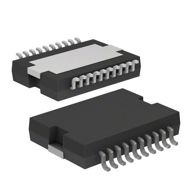
PowerSO20
ORDERING NUMBER: L9825
DESCRIPTION
L9825 is a Octal Low-Side Driver Circuit, dedicated
for automotive applications. Output voltage clamping
is provided for flyback current recirculation, when inductive loads are driven. Chip Select and Serial Peripheral Interface for outputs control and diagnostic
data transfer. Parallel Control inputs for two outputs.
BLOCK DIAGRAM
VCC
VCC
OUT1
NON1
1
3
S
2
IOL
Latch / Driver
Q1
R
+
Fault Latch
Diag1
-
VDG
CH1
NON2
CLK
VCC
SDI
VCC
SDO
OUT2
OUT3
Output Latch
VCC
SPI
Interface
NCS
CH2
Q2
Diag2
Shift Register
VCC
Q1
Q2
Q3
Q4
Q5
Q6
Q7
Q8
Q3
S
Latch / Driver
IOL
R
+
Diag1 Diag3
Diag2
Diag3
Q4
Diag4 Diag4
Diag5
Q5
Diag6
Diag5
Diag7
Q6
Diag8
Diag6
-
VDG
CH3
CH4
CH5
CH6
OUT4
OUT5
OUT6
OUT7
Q7
VCC
nRES
VCC
Reset
S Latch / Driver
Current Control
IOL
R
Reset
Overtemperature Detection
+
Undervoltage
RESET
Diag7
Q8
Diag8
-
VDG
CH7
CH8
OUT8
GND
September 2013
1/11
�L9825
PIN CONNECTION (Top view)
GND
1
20
NON1
2
19
NCS
SDO
3
18
nRes
OUT1
4
17
OUT8
OUT3
5
16
OUT6
OUT5
6
15
OUT4
OUT7
7
14
OUT2
SDI
8
13
Vcc
CLK
9
12
NON2
GND
10
11
GND
POWSO20
PIN DESCRIPTION
N°
Pin
1
GND
device ground
2
NON1
control input 1
3
SDO
serial data output
4
Out 1
output 1
5
Out 3
output 3
6
Out 5
output 5
7
Out 7
output 7
8
SDI
serial data input
9
CLK
serial clock
10
GND
device ground
11
GND
device ground
12
NON2
control input 2
13
VCC
supply voltage
14
Out 2
output 2
15
Out 4
output 4
16
Out 6
output 6
17
Out 8
output 8
18
nRes
asynchronous nRes
19
NCS
chip select (active low)
20
GND
device ground
2/11
Function
GND
�L9825
ABSOLUTE MAXIMUM RATINGS
For voltages and currents applied externally to the device:
Symbol
VCC
Parameter
Supply voltage
Value
Unit
-0.3 to 7
V
Inputs and data lines (NONx, NCS, CLK, SDI, nRes)
VIN
Voltage (NONx, NCS, CLK, SDI)
-0.3 to 7
V
VIN
Voltage (nRes)
-0.3 to 7
V
IIN
Protection diodes current 1)
(T ≤ 1ms)
-20 to 20
mA
Continuous output voltage
-1.0 to 45
V
Output current 2)
-3 to 2.05
A
20
mJ
Outputs (Out1 ... Out8)
VOUTc
IOUT
EOUTcl
Output clamp energy (IOUT ≤ 0.5A)
Notes: 1. All inputs are protected against ESD according to MIL 883C; tested with HBM at 2KV. It corresponds to a dissipated energy
E ≤ 0,2mJ.
2. Transient pulses in accordance to DIN40839 part 1, 3 and ISO 7637 Part 1, 3.
For currents determined within the device:
Outputs (Out1 ... Out8)
IOUT
Output current (Out1 ... Out6)
2.05
A
IOUT
Output current (Out7, Out8)
1.75
A
4.5 (Min.)
A
Total average-current all outputs 3)
3. When operating the device with short circuit at more than 2 outputs at the same time, damage due to electrical overstress may
occur.
THERMAL DATA
Symbol
Parameter
Value
Unit
150
165
°C
°C
Thermal shutdown
TJSC
Thermal shutdown threshold
Min.
Typ.
Thermal resistance
Rthjc-one
Single output (junction case) Max.
13
°C/W
Rthjc-all
All outputs (junction case) Max.
1.6
°C/W
3/11
�L9825
ELECTRICAL CHARACTERISTCS
(4.5V ≤ VCC ≤ 5.5V; -40°C ≤ TJ ≤ 150°C; unless otherwise specified)
Symbol
Parameter
Test Condition
Min.
Typ.
Max.
Unit
Supply voltage
IccSTB
Standby current
without load
5
mA
IccOPM
Operating mode
IOUT1 ... 8 = 500mA
SPI - CLK = 3MHz
NCS = LOW
SDO no load
5
mA
ΔICC during reverse output
current
Iout = -3A
100
mA
ΔICC
Inputs (NONx. NCS, CLK, SDI, nRes)
VINL
Low level
-0.3
0.2·VCC
V
VINH
High level
0.7·VCC
VCC+0.3
V
Vhyst
Hysteresis voltage
IIN
Input current
RIN
Pullup resistance
CIN
Input capacitance
0.85
V
VIN = VCC
50
10
µA
250
kΩ
10
pF
Serial data outputs
VSDOH
High output level
ISDO = -4mA
VSDOL
Low output level
ISDO = 3,2mA
ISDOL
Tristate leakage current
NCS = high; 0V ≤ VSDO ≤ VCC
CSDO
Output capacitance
VCC -0.4
V
0.4
V
10
µA
fSDO = 300kHz
10
pF
IOUTL1 - 8 Leakage current
OUTx = OFF; VOUTx = 25V; VCC
= 5V
100
µA
IOUTL1 - 8 Leakage current
OUTx = OFF; VOUTx = 16V; VCC
= 5V
100
µA
IOUTL1 - 8 Leakage current
OUTx = OFF; VOUTx = 16V; VCC
= 1V
10
µA
60
V
-10
Outputs OUT 1 ... 8
Output clamp voltage
1mA ≤ Iclp ≤ Ioutp; Itest = 10mA
with correlation
RDSon
On resistance OUT 1 ... 8
IOUT = 500mA; Tj = +150°C
1.5
W
COUT
Output capacitance
VOUT = 16V; f = 1MHz
300
pF
Vclp
45
Outputs short circuit protection
ISBC
Overcurrent shutoff threshold
OUT1 ... OUT6
1.05
1.4
2.05
A
ILIM
Short circuit current limitation
OUT7; OUT8
1.05
1.4
1.75
A
tSCB
Delay shutdown
for output 1 ... 6; IOUT ≤ 1/2 ISBC
0.2
3
12
µs
4/11
�L9825
ELECTRICAL CHARACTERISTCS (continued)
(4.5V ≤ VCC ≤ 5.5V; -40°C ≤ TJ ≤ 150°C; unless otherwise specified)
Symbol
Parameter
Test Condition
Min.
Typ.
Max.
Unit
0.32·VCC
0.4·VCC
V
20
100
µA
15
50
µs
Diagnostics
VDG
Diagnostic threshold voltage
IOL
Open load detection sink current
tdf
Diagnostic detection filter time for
output 1 & 2 on each diagnostic
condition
Vout = VDG
Outputs timing
tdon1
Turn ON delay of OUT 1 and 2
NON1, 2 = 50% to VOUT = 0.9·Vbat
NCS = 50% to VOUT = 0.9·Vbat
5
µs
tdon2
Turn ON delay of OUT 3 to 8
NCS = 50% to VOUT = 0.9·Vbat
10
µs
tdoff
Turn OFF delay of OUT 1 to 8
NCS = 50% to VOUT = 0.1·Vbat
NON1, 2 = 50% to VOUT = 0.1·Vbat
10
µs
dUon1/dt Turn ON voltage slew-rate
For output 3 to 8; 90% to 30% of
Vbat; RL = 500Ω; Vbat = 16V
0.7
3.5
V/µs
dUon2/dt Turn ON voltage slew-rate
For output 1 and 2; 90% to 30%
of Vbat; RL = 500Ω; Vbat = 16V
2
10
V/µs
dUoff1/dt Turn OFF voltage slew-rate
For output 1 to 8; 30% to 90% of
Vbat; RL = 500Ω; Vbat = 16V
2
10
V/µs
dUoff2/dt Turn OFF voltage slew-rate
For output 1 to 8; 30% to 80% of
Vbat; RL = 500Ω; Vbat = 0.9 · Vclp
2
15
V/µs
Serial diagnostic link (Load capacitor at SDO = 100pF)
fclk
Clock frequency
tclh
tcll
50% duty cycle
3
MHz
Minimum time CLK = HIGH
160
ns
Minimum time CLK = LOW
160
ns
4.9V ≤ VCC ≤ 5.1V
tpcld
Propagation delay
CLK to data at SDO valid
tcsdv
NCS = LOW to data at SDO
active
tsclch
CLK low before NCS low
thclcl
CLK change L/H after NCS = low
tscld
SDI input setup time
CLK change H/L after SDI data
valid
thcld
SDI input hold time
SDI data hold after CLK change H/L
tsclcl
CLK low before NCS high
150
ns
thclch
CLK high after NCS high
150
ns
tpchdz
NCS L/H to output data float
NCS pulse filter time
Setup time CLK to NCS change H/L
100
ns
100
ns
100
ns
100
ns
20
ns
20
100
ns
ns
Multiple of 8 CLK cycles
5/11
�L9825
FUNCTIONAL DESCRIPTION
General
The L9825 integrated circuit features 8 power low-side-driver outputs. Data is transmitted to the device using
the Serial Peripheral Interface, SPI protocol. Outputs 1 and 2 can be controlled parallel or serial. The power
outputs features voltage clamping function for flyback current recirculation and are protected against short circuit to Vbat.
The diagnostics recognizes two outputs fault conditions: 1) overcurrent for outputs 1 to 6 , overcurrent and thermal overload for outputs 7 and 8 in switch-on condition and 2) open load or short to GND in switch-off condition
for all outputs. The outputs status can be read out via the serial interface.
The chip internal reset is a OR function of the external nRes signal and internally generated undervoltage nRes
signal.
Output Stages Control
Each output is controlled with its latch and with common reset line, which enables all eight outputs. Outputs 1
and 2 can be controlled also by its NON1, NON2 inputs. It allows PWM control independently on the SPI. These
inputs features internal pull-up resistors to assure that the outputs are switched off, when the inputs are open.
The control data are transmitted via the SDI input, the timing of the serial interface is shown in Fig. 1.
The device is selected with low NCS signal and the input data are transferred into the 8 bit shift register at every
falling CLK edge. The rising edge of the NCS latches the new data from the shift register to the drivers.
Figure 1. Timing of the Serial Interface
NCS
tsclch
thclcl
tclh
tcll
tsclcl
thclch
CLK
tcsdv
SDO
tpcld
tpchdz
not defined
D8
D1
thcld
tscld
SDI
D8
D7
D1
The SPI register data are transferred to the output latch at rising NCS edge. The digital filter between NCS and
the output latch ensures that the data are transferred only after 8 CLK cycles or multiple of 8 CLK cycles since
the last NCS falling edge. The NCS changes only at low CLK.
Table 1. Outputs Control
Outputs 1, 2:
Outputs 3 to 8:
NON1,2
1
0
0
1
SPI-bit 1,2
0
0
1
1
SPI-bit 3...8
0
1
Output 1, 2
off
on
on
on
Output 3...8
off
on
6/11
�L9825
Figure 2. Output Control register structure
MSB
LSB
Q2 Q4 Q6 Q8 Q1 Q3 Q5 Q7
Control-bit output 7
Control-bit output 5
Control-bit output 3
Control-bit output 1
Control-bit output 8
Control-bit output 6
Control-bit output 4
Control-bit output 2
Power outputs characteristics for flyback current, outputs short circuit protection and diagnostics
For output currents flowing into the circuit the output voltages are limited. The typical value of this voltage is 50V.
This function allows that the flyback current of a inductive load recirculates into the circuit; the flyback energy is
absorbed in the chip.
Output short circuit protection for outputs 1 to 6 (dedicated for loads without inrush current): when the output
current exceeds the short circuit threshold, the corresponding output overload latch is set and the output is
switched off immediately.
Output short circuit protection for outputs 7 and 8 (dedicated for loads with inrush current, as lamps): when the
load current would exceed the short circuit limit value, the corresponding output goes in a current regulation
mode. The output current is determined by the output characteristics and the output voltage depends on the
load resistance. In this mode high power is dissipated in the output transistor and its temperature increases rapidly. When the power transistor temperature exceeds the thermal shutdown threshold, the overload latch is set
and the corresponding output switched off.
For the load diagnostic in output off condition each output features a diagnostic current sink, typ 60µA.
Diagnostics
The output voltage at all outputs is compared with the diagnostic threshold, typ 0.38 · VCC.
Outputs 1 and 2 features dedicated fault latches. The output status signal is filtered and latched. The fault latches are cleared during NCS low. The latch stores the status bit, so the first reading after the error occurred might
be wrong. The second reading is right.
Table 2. Diagnostic for outputs 1 and 2 in parallel controlled mode.
Output 1, 2
Output-voltage
Status-bit
Output-mode
off
> DG-threshold
high
correct operation
off
< DG-threshold
low
fault condition 2)
on
< DG-threshold
high
correct operation
on
> DG-threshold
low
fault condition 1)
Fault condition 1) "output short circuit to Vbat" : the output was switched on and the voltage at the output exceeded the diagnostics threshold due to overcurrent, the output overload latch was set and the output has been
switched off. The diagnostic bit is low.
7/11
�L9825
Fault condition 2) "open load" or "output short circuit to GND" : the output is switched off and the voltage at the
output drops below the diagnostics threshold, because the load current is lower than the output diagnostic current source, the load is interrupted. The diagnostic bit is low.
For outputs 3 to 8 the output status signals, are fed directly to the SPI register.
Table 3. Diagnostic for outputs 1 to 8 in SPI controlled mode.
Output 1 ... 8
Output-voltage
Status-bit
Output-mode
off
> DG-threshold
high
correct operation
off
< DG-threshold
low
fault condition 2)
on
< DG-threshold
low
correct operation
on
> DG-threshold
high
fault condition 1)
The fault condition 1) "output short circuit to Vbat" :
For outputs 3 to 6 is the same as of outputs 1 and 2.
For outputs 7 and 8 : the output was switched on and the voltage at the output exceeds the diagnostics threshold. The output operates in current regulation mode or has been switched off due to thermal shutdown. The status bit is low.
Fault condition 2) "open load" or "output short circuit to GND" is the same as of outputs 1 and 2.
At the falling edge of NCS the output status data are transferred to the shift register. When NSC is low, data bits
contained in the shift register are transferred to SDO output et every rising CLK edge.
Figure 3. The Pulse Diagram to Read the Outputs Status Register
NCS
CLK
SDI
MSB
6
MSB
SDO
5
6
4
5
3
4
2
3
LSB
1
2
1
LSB
Figure 4. The Structure of the Outputs Status Register
MSB
LSB
Diag2 Diag4 Diag6 Diag8 Diag1 Diag3 Diag5 Diag7
Diagnostic-bit output 7
Diagnostic-bit output 5
Diagnostic-bit output 3
Diagnostic-bit output 1
Diagnostic-bit output 8
Diagnostic-bit output 6
Diagnostic-bit output 4
Diagnostic-bit output 2
8/11
�L9825
APPLICATION NOTES
Figure 5. Typical Application Circuit Diagram
L9825
L9825
For higher current driving capability two outputs of the same kind can be paralleled. In this case the maximum
flyback energy should not exceed the limit value for single output.
The immunity of the circuit with respect to the transients at the output is verified during the characterization for
Test Pulses 1, 2 and 3a, 3b, DIN40839 or ISO7637 part 3. The Test Pulses are coupled to the outputs with
200pF series capacitor. All outputs withstand testpulses without damage.
The correct function of the circuit with the Test Pulses coupled to the outputs is verified during the characterization for the typical application with R = 16W to 200W, L= 0 to 600mH loads. The Test Pulses are coupled to
the outputs with 200pF series capacitor.
9/11
�L9825
DIM.
mm
MIN.
TYP.
A
a1
inch
MAX.
MIN.
TYP.
3.6
0.1
0.3
a2
0.142
0.004
0.012
3.3
0.130
a3
0
0.1
0.000
0.004
b
0.4
0.53
0.016
0.021
c
0.23
0.32
0.009
0.013
D (1)
15.8
16
0.622
0.630
0.386
D1 (2)
9.4
9.8
0.370
E
13.9
14.5
0.547
e
1.27
e3
E1 (1)
0.570
0.450
11.1
E2
0.429
0.437
2.9
0.114
E3
5.8
6.2
0.228
G
0
0.1
0.000
0.004
H
15.5
15.9
0.610
0.626
0.031
0.043
h
L
0.244
1.1
0.8
1.1
0.043
N
8˚(typ.)
S
8˚(max. )
T
Weight: 1.9gr
0.050
11.43
10.9
OUTLINE AND
MECHANICAL DATA
MAX.
10
JEDEC MO-166
0.394
PowerSO-20
(1) “D and E1” do not include mold flash or protusions.
- Mold flash or protusions shall not exceed 0.15mm (0.006”)
- Critical dimensions: “E”, “G” and “a3”.
(2) For subcontractors, the limit is the one quoted in jedec MO-166
N
R
N
a2
b
A
e
DETAIL A
c
a1
DETAIL B
E
e3
H
DETAIL A
lead
D
slug
a3
DETAIL B
20
11
0.35
Gage Plane
-C-
S
SEATING PLANE
L
G
E2
E1
BOTTOM VIEW
C
(COPLANARITY)
T
E3
1
h x 45˚
1
0
PSO20MEC
D1
0056635 I
10/11
�L9825
Please Read Carefully:
Information in this document is provided solely in connection with ST products. STMicroelectronics NV and its subsidiaries (“ST”) reserve the
right to make changes, corrections, modifications or improvements, to this document, and the products and services described herein at any
time, without notice.
All ST products are sold pursuant to ST’s terms and conditions of sale.
Purchasers are solely responsible for the choice, selection and use of the ST products and services described herein, and ST assumes no
liability whatsoever relating to the choice, selection or use of the ST products and services described herein.
No license, express or implied, by estoppel or otherwise, to any intellectual property rights is granted under this document. If any part of this
document refers to any third party products or services it shall not be deemed a license grant by ST for the use of such third party products
or services, or any intellectual property contained therein or considered as a warranty covering the use in any manner whatsoever of such
third party products or services or any intellectual property contained therein.
UNLESS OTHERWISE SET FORTH IN ST’S TERMS AND CONDITIONS OF SALE ST DISCLAIMS ANY EXPRESS OR IMPLIED
WARRANTY WITH RESPECT TO THE USE AND/OR SALE OF ST PRODUCTS INCLUDING WITHOUT LIMITATION IMPLIED
WARRANTIES OF MERCHANTABILITY, FITNESS FOR A PARTICULAR PURPOSE (AND THEIR EQUIVALENTS UNDER THE LAWS
OF ANY JURISDICTION), OR INFRINGEMENT OF ANY PATENT, COPYRIGHT OR OTHER INTELLECTUAL PROPERTY RIGHT.
ST PRODUCTS ARE NOT DESIGNED OR AUTHORIZED FOR USE IN: (A) SAFETY CRITICAL APPLICATIONS SUCH AS LIFE
SUPPORTING, ACTIVE IMPLANTED DEVICES OR SYSTEMS WITH PRODUCT FUNCTIONAL SAFETY REQUIREMENTS; (B)
AERONAUTIC APPLICATIONS; (C) AUTOMOTIVE APPLICATIONS OR ENVIRONMENTS, AND/OR (D) AEROSPACE APPLICATIONS
OR ENVIRONMENTS. WHERE ST PRODUCTS ARE NOT DESIGNED FOR SUCH USE, THE PURCHASER SHALL USE PRODUCTS AT
PURCHASER’S SOLE RISK, EVEN IF ST HAS BEEN INFORMED IN WRITING OF SUCH USAGE, UNLESS A PRODUCT IS
EXPRESSLY DESIGNATED BY ST AS BEING INTENDED FOR “AUTOMOTIVE, AUTOMOTIVE SAFETY OR MEDICAL” INDUSTRY
DOMAINS ACCORDING TO ST PRODUCT DESIGN SPECIFICATIONS. PRODUCTS FORMALLY ESCC, QML OR JAN QUALIFIED ARE
DEEMED SUITABLE FOR USE IN AEROSPACE BY THE CORRESPONDING GOVERNMENTAL AGENCY.
Resale of ST products with provisions different from the statements and/or technical features set forth in this document shall immediately void
any warranty granted by ST for the ST product or service described herein and shall not create or extend in any manner whatsoever, any
liability of ST.
ST and the ST logo are trademarks or registered trademarks of ST in various countries.
Information in this document supersedes and replaces all information previously supplied.
The ST logo is a registered trademark of STMicroelectronics. All other names are the property of their respective owners.
© 2013 STMicroelectronics - All rights reserved
STMicroelectronics group of companies
Australia - Belgium - Brazil - Canada - China - Czech Republic - Finland - France - Germany - Hong Kong - India - Israel - Italy - Japan Malaysia - Malta - Morocco - Philippines - Singapore - Spain - Sweden - Switzerland - United Kingdom - United States of America
www.st.com
DocID8027 Rev 3
11/11
11
�