L99ASC03
Brushless / sensorless 3-phase motor pre-driver
for automotive applications
Datasheet - production data
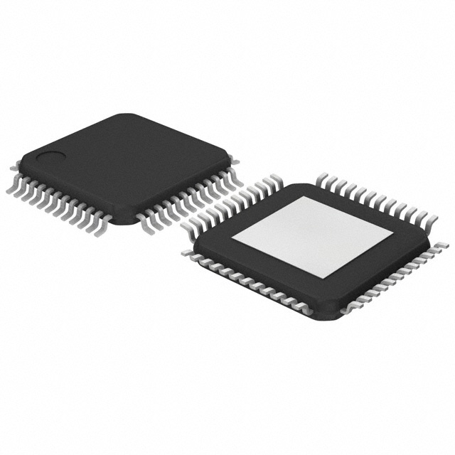
• TQFP48 7 x 7 x 1 mm with Exposed Pad
(4.5 x 4.5 mm) package
Applications
• Mechatronic three-phase motor application
such as engine cooling fans, fuel pumps, water
pumps, oil pumps
TQFP48-EP
Features
Description
• Automotive qualified
The L99ASC03 is a multifunctional system IC
designed for three-phase motor control
applications.
• 5 V low-drop voltage regulator (200 mA
continuous mode)
• Very low current consumption in standby mode
(typ. 15 µA)
• ST SPI interface for control and diagnostics
• Window watchdog and fail-safe functionality
• Two separate power supply pins
• Three half-bridge drivers to control external
MOSFETs (configurable by SPI)
• Full drive of external MOSFETs down to 6 V
input voltage
• Input pin for each gate driver (with crosscurrent protection)
The device features a voltage regulator to supply
an external microcontroller and an operation
amplifier for motor current sensing. It is designed
to control six external
N-channel MOSFETs in bridge configuration to
drive three-phase motors in automotive
applications. All gate driver outputs are controlled
by separate inputs.
The integrated Serial Peripheral Interface (SPI)
makes it possible to adjust device parameters,
control all operating modes and read out
diagnostic information.
• Two-stage charge pump supporting 100% duty
cycle
• PWM operation up to 80 kHz (not restricted)
• Current-sense amplifier (configurable by SPI)
• Disable input to turn off gate driver outputs
• Analog multiplexer output to monitor external
power supply voltages and internal junction
temperature
• Advanced BEMF detection IP
• Overcurrent protection (programmable)
• Drain-source monitoring and open-load
detection
August 2015
This is information on a product in full production.
Table 1. Device summary
Order codes
Package
TQFP48-EP
DocID023504 Rev 7
Tube
Tape and real
L99ASC03
L99ASC03TR
1/73
www.st.com
�Contents
L99ASC03
Contents
1
Block diagram and pin descriptions . . . . . . . . . . . . . . . . . . . . . . . . . . . . 7
2
Device description . . . . . . . . . . . . . . . . . . . . . . . . . . . . . . . . . . . . . . . . . 10
2.1
Supply pins (VS, VSREG, VSMS) . . . . . . . . . . . . . . . . . . . . . . . . . . . . . . . . 10
2.1.1
VS, VSREG and VSMS overvoltage warning . . . . . . . . . . . . . . . . . . . . . . 10
2.1.2
VS, VSREG and VSMS overvoltage . . . . . . . . . . . . . . . . . . . . . . . . . . . . . 10
2.1.3
VS, VSREG and VSMS undervoltage . . . . . . . . . . . . . . . . . . . . . . . . . . . . 10
2.2
VDD (5V) voltage regulator . . . . . . . . . . . . . . . . . . . . . . . . . . . . . . . . . . . . 10
2.3
NRES reset output . . . . . . . . . . . . . . . . . . . . . . . . . . . . . . . . . . . . . . . . . . .11
2.4
Watchdog . . . . . . . . . . . . . . . . . . . . . . . . . . . . . . . . . . . . . . . . . . . . . . . . . 12
2.5
Device operating modes . . . . . . . . . . . . . . . . . . . . . . . . . . . . . . . . . . . . . . 14
2.5.1
Active Mode . . . . . . . . . . . . . . . . . . . . . . . . . . . . . . . . . . . . . . . . . . . . . . 14
2.5.2
Flash Mode . . . . . . . . . . . . . . . . . . . . . . . . . . . . . . . . . . . . . . . . . . . . . . 14
2.5.3
VDD Standby Mode . . . . . . . . . . . . . . . . . . . . . . . . . . . . . . . . . . . . . . . . 15
2.5.4
VBAT Standby Mode . . . . . . . . . . . . . . . . . . . . . . . . . . . . . . . . . . . . . . . 15
2.5.5
Device mode state diagram . . . . . . . . . . . . . . . . . . . . . . . . . . . . . . . . . . 16
2.5.6
Functional overview . . . . . . . . . . . . . . . . . . . . . . . . . . . . . . . . . . . . . . . . 17
2.6
DIS pin . . . . . . . . . . . . . . . . . . . . . . . . . . . . . . . . . . . . . . . . . . . . . . . . . . . 17
2.7
INH pin . . . . . . . . . . . . . . . . . . . . . . . . . . . . . . . . . . . . . . . . . . . . . . . . . . . 17
2.8
Thermal warning and thermal shutdown . . . . . . . . . . . . . . . . . . . . . . . . . 17
2.8.1
Normal mode: TEMPM = ‘0’ (TW1, TSD1, TSD2) . . . . . . . . . . . . . . . . . 18
2.8.2
Warning mode: TEMP = ‘1’ (TW1, TW2, TSD2) . . . . . . . . . . . . . . . . . . 18
2.9
Wake-up events . . . . . . . . . . . . . . . . . . . . . . . . . . . . . . . . . . . . . . . . . . . . 20
2.10
Charge pump . . . . . . . . . . . . . . . . . . . . . . . . . . . . . . . . . . . . . . . . . . . . . . 20
2.11
Gate drivers . . . . . . . . . . . . . . . . . . . . . . . . . . . . . . . . . . . . . . . . . . . . . . . 20
2.12
Drain-source monitoring . . . . . . . . . . . . . . . . . . . . . . . . . . . . . . . . . . . . . . 22
2.12.1
Drain-source monitoring in ON state (short-circuit detection) . . . . . . . . 22
2.12.2
Drain-source monitoring in OFF state (open-load / short-circuit detection)
. . . . . . . . . . . . . . . . . . . . . . . . . . . . . . . . . . . . . . . . . . . . . . . . . . . . . . . . 22
2.13
Current-sense amplifier . . . . . . . . . . . . . . . . . . . . . . . . . . . . . . . . . . . . . . 23
2.14
Overcurrent detection . . . . . . . . . . . . . . . . . . . . . . . . . . . . . . . . . . . . . . . . 23
2.15
BEMF module . . . . . . . . . . . . . . . . . . . . . . . . . . . . . . . . . . . . . . . . . . . . . . 23
2.15.1
2/73
BEMF comparator . . . . . . . . . . . . . . . . . . . . . . . . . . . . . . . . . . . . . . . . . 23
DocID023504 Rev 7
�L99ASC03
3
4
Contents
2.15.2
BEMF comparator sampling . . . . . . . . . . . . . . . . . . . . . . . . . . . . . . . . . 24
2.15.3
BEMF commutation driving mode . . . . . . . . . . . . . . . . . . . . . . . . . . . . . 24
2.16
Digital multiplexer (DOUT) . . . . . . . . . . . . . . . . . . . . . . . . . . . . . . . . . . . . 24
2.17
Analog multiplexer (AOUT) . . . . . . . . . . . . . . . . . . . . . . . . . . . . . . . . . . . 24
2.18
Diagnostics . . . . . . . . . . . . . . . . . . . . . . . . . . . . . . . . . . . . . . . . . . . . . . . . 25
2.19
Serial peripheral interface (ST SPI standard) . . . . . . . . . . . . . . . . . . . . . . 29
Electrical specifications . . . . . . . . . . . . . . . . . . . . . . . . . . . . . . . . . . . . . 31
3.1
Absolute maximum ratings . . . . . . . . . . . . . . . . . . . . . . . . . . . . . . . . . . . . 31
3.2
Operating range . . . . . . . . . . . . . . . . . . . . . . . . . . . . . . . . . . . . . . . . . . . . 31
3.3
ESD protection . . . . . . . . . . . . . . . . . . . . . . . . . . . . . . . . . . . . . . . . . . . . . 32
3.4
Thermal data . . . . . . . . . . . . . . . . . . . . . . . . . . . . . . . . . . . . . . . . . . . . . . 32
3.5
Electrical characteristics . . . . . . . . . . . . . . . . . . . . . . . . . . . . . . . . . . . . . . 33
3.6
SPI electrical characteristics . . . . . . . . . . . . . . . . . . . . . . . . . . . . . . . . . . 43
ST-SPI Protocol . . . . . . . . . . . . . . . . . . . . . . . . . . . . . . . . . . . . . . . . . . . . 46
4.1
4.2
4.3
Physical layer . . . . . . . . . . . . . . . . . . . . . . . . . . . . . . . . . . . . . . . . . . . . . . 46
4.1.1
Signal description . . . . . . . . . . . . . . . . . . . . . . . . . . . . . . . . . . . . . . . . . 46
4.1.2
Clock and data characteristics . . . . . . . . . . . . . . . . . . . . . . . . . . . . . . . . 46
Protocol . . . . . . . . . . . . . . . . . . . . . . . . . . . . . . . . . . . . . . . . . . . . . . . . . . 47
4.2.1
SDI frame . . . . . . . . . . . . . . . . . . . . . . . . . . . . . . . . . . . . . . . . . . . . . . . . 47
4.2.2
SDO frame . . . . . . . . . . . . . . . . . . . . . . . . . . . . . . . . . . . . . . . . . . . . . . . 50
Addresses and data definition . . . . . . . . . . . . . . . . . . . . . . . . . . . . . . . . . 50
4.3.1
4.4
Device information registers . . . . . . . . . . . . . . . . . . . . . . . . . . . . . . . . . 50
SPI registers . . . . . . . . . . . . . . . . . . . . . . . . . . . . . . . . . . . . . . . . . . . . . . . 52
4.4.1
SPI Control Registers . . . . . . . . . . . . . . . . . . . . . . . . . . . . . . . . . . . . . . 53
4.4.2
Device Control Register 1 . . . . . . . . . . . . . . . . . . . . . . . . . . . . . . . . . . . 54
4.4.3
Device Control Register 2 . . . . . . . . . . . . . . . . . . . . . . . . . . . . . . . . . . . 55
4.4.4
Device Control Register 3 . . . . . . . . . . . . . . . . . . . . . . . . . . . . . . . . . . . 56
4.4.5
Device Control Register 4 . . . . . . . . . . . . . . . . . . . . . . . . . . . . . . . . . . . 58
4.4.6
Device Control Register 5 . . . . . . . . . . . . . . . . . . . . . . . . . . . . . . . . . . . 59
4.4.7
Device Control Register 6 . . . . . . . . . . . . . . . . . . . . . . . . . . . . . . . . . . . 60
4.4.8
Device Control Register 7 . . . . . . . . . . . . . . . . . . . . . . . . . . . . . . . . . . . 61
4.4.9
Device Control Register 8 . . . . . . . . . . . . . . . . . . . . . . . . . . . . . . . . . . . 62
4.4.10
Device Status Registers 1 . . . . . . . . . . . . . . . . . . . . . . . . . . . . . . . . . . . 62
4.4.11
Device Status Registers 2 . . . . . . . . . . . . . . . . . . . . . . . . . . . . . . . . . . . 63
DocID023504 Rev 7
3/73
4
�Contents
5
6
4/73
L99ASC03
4.4.12
Device Status Registers 3 . . . . . . . . . . . . . . . . . . . . . . . . . . . . . . . . . . . 64
4.4.13
Device Status Registers 4 . . . . . . . . . . . . . . . . . . . . . . . . . . . . . . . . . . . 64
4.4.14
Device Status Registers 5 . . . . . . . . . . . . . . . . . . . . . . . . . . . . . . . . . . . 65
4.4.15
Device Status Registers 6 . . . . . . . . . . . . . . . . . . . . . . . . . . . . . . . . . . . 65
4.4.16
Device Status Registers 7 . . . . . . . . . . . . . . . . . . . . . . . . . . . . . . . . . . . 66
Package information . . . . . . . . . . . . . . . . . . . . . . . . . . . . . . . . . . . . . . . . 67
5.1
ECOPACK® packages . . . . . . . . . . . . . . . . . . . . . . . . . . . . . . . . . . . . . . . 67
5.2
TQFP48-EP mechanical data . . . . . . . . . . . . . . . . . . . . . . . . . . . . . . . . . . 67
Revision history . . . . . . . . . . . . . . . . . . . . . . . . . . . . . . . . . . . . . . . . . . . 69
DocID023504 Rev 7
�L99ASC03
List of tables
List of tables
Table 1.
Table 2.
Table 3.
Table 4.
Table 5.
Table 6.
Table 7.
Table 8.
Table 9.
Table 10.
Table 11.
Table 12.
Table 13.
Table 14.
Table 15.
Table 16.
Table 17.
Table 18.
Table 19.
Table 20.
Table 21.
Table 22.
Table 23.
Table 24.
Table 25.
Table 26.
Table 27.
Table 28.
Table 29.
Table 30.
Table 31.
Table 32.
Table 33.
Table 34.
Table 35.
Table 36.
Table 37.
Table 38.
Table 39.
Device summary . . . . . . . . . . . . . . . . . . . . . . . . . . . . . . . . . . . . . . . . . . . . . . . . . . . . . . . . . . 1
Pin definition and function. . . . . . . . . . . . . . . . . . . . . . . . . . . . . . . . . . . . . . . . . . . . . . . . . . . 7
Functional overview . . . . . . . . . . . . . . . . . . . . . . . . . . . . . . . . . . . . . . . . . . . . . . . . . . . . . . 17
Wake-up events . . . . . . . . . . . . . . . . . . . . . . . . . . . . . . . . . . . . . . . . . . . . . . . . . . . . . . . . . 20
Diagnostics overview . . . . . . . . . . . . . . . . . . . . . . . . . . . . . . . . . . . . . . . . . . . . . . . . . . . . . 25
Forced VBAT standby mode . . . . . . . . . . . . . . . . . . . . . . . . . . . . . . . . . . . . . . . . . . . . . . . . 28
Absolute maximum ratings . . . . . . . . . . . . . . . . . . . . . . . . . . . . . . . . . . . . . . . . . . . . . . . . . 31
Operating range . . . . . . . . . . . . . . . . . . . . . . . . . . . . . . . . . . . . . . . . . . . . . . . . . . . . . . . . . 31
ESD protection . . . . . . . . . . . . . . . . . . . . . . . . . . . . . . . . . . . . . . . . . . . . . . . . . . . . . . . . . . 32
Operation junction temperature . . . . . . . . . . . . . . . . . . . . . . . . . . . . . . . . . . . . . . . . . . . . . 32
Temperature warning and thermal shutdown . . . . . . . . . . . . . . . . . . . . . . . . . . . . . . . . . . . 32
Supply and supply monitoring. . . . . . . . . . . . . . . . . . . . . . . . . . . . . . . . . . . . . . . . . . . . . . . 33
Power-on RESET (VSREG) . . . . . . . . . . . . . . . . . . . . . . . . . . . . . . . . . . . . . . . . . . . . . . . . . 34
Voltage regulator VDD . . . . . . . . . . . . . . . . . . . . . . . . . . . . . . . . . . . . . . . . . . . . . . . . . . . . . 34
NRES reset output (VDD supervision), NINT . . . . . . . . . . . . . . . . . . . . . . . . . . . . . . . . . . . 35
Watchdog . . . . . . . . . . . . . . . . . . . . . . . . . . . . . . . . . . . . . . . . . . . . . . . . . . . . . . . . . . . . . . 36
Charge pump output . . . . . . . . . . . . . . . . . . . . . . . . . . . . . . . . . . . . . . . . . . . . . . . . . . . . . . 37
Gate driver for external MOSFET . . . . . . . . . . . . . . . . . . . . . . . . . . . . . . . . . . . . . . . . . . . . 37
Drain source monitoring . . . . . . . . . . . . . . . . . . . . . . . . . . . . . . . . . . . . . . . . . . . . . . . . . . . 40
VS, VSREG, VSMS and Tj monitoring (AOUT) . . . . . . . . . . . . . . . . . . . . . . . . . . . . . . . . . . . 41
Current-sense amplifier . . . . . . . . . . . . . . . . . . . . . . . . . . . . . . . . . . . . . . . . . . . . . . . . . . . 41
Overcurrent detection . . . . . . . . . . . . . . . . . . . . . . . . . . . . . . . . . . . . . . . . . . . . . . . . . . . . . 41
BEMF detection . . . . . . . . . . . . . . . . . . . . . . . . . . . . . . . . . . . . . . . . . . . . . . . . . . . . . . . . . 42
I/Os; IHx, ILx, DIS, BC, BEMF, DOUT . . . . . . . . . . . . . . . . . . . . . . . . . . . . . . . . . . . . . . . . 42
INH input . . . . . . . . . . . . . . . . . . . . . . . . . . . . . . . . . . . . . . . . . . . . . . . . . . . . . . . . . . . . . . . 43
CSN input . . . . . . . . . . . . . . . . . . . . . . . . . . . . . . . . . . . . . . . . . . . . . . . . . . . . . . . . . . . . . . 43
SCK, SDI input . . . . . . . . . . . . . . . . . . . . . . . . . . . . . . . . . . . . . . . . . . . . . . . . . . . . . . . . . . 43
SDO output . . . . . . . . . . . . . . . . . . . . . . . . . . . . . . . . . . . . . . . . . . . . . . . . . . . . . . . . . . . . . 43
SPI timing . . . . . . . . . . . . . . . . . . . . . . . . . . . . . . . . . . . . . . . . . . . . . . . . . . . . . . . . . . . . . . 44
SPI pin description . . . . . . . . . . . . . . . . . . . . . . . . . . . . . . . . . . . . . . . . . . . . . . . . . . . . . . . 46
Operation codes . . . . . . . . . . . . . . . . . . . . . . . . . . . . . . . . . . . . . . . . . . . . . . . . . . . . . . . . . 48
Device application access . . . . . . . . . . . . . . . . . . . . . . . . . . . . . . . . . . . . . . . . . . . . . . . . . 49
Device information read access . . . . . . . . . . . . . . . . . . . . . . . . . . . . . . . . . . . . . . . . . . . . . 49
Address range . . . . . . . . . . . . . . . . . . . . . . . . . . . . . . . . . . . . . . . . . . . . . . . . . . . . . . . . . . 49
Device information read access operation code . . . . . . . . . . . . . . . . . . . . . . . . . . . . . . . . . 51
Device information registers . . . . . . . . . . . . . . . . . . . . . . . . . . . . . . . . . . . . . . . . . . . . . . . . 51
Complete device SPI register table . . . . . . . . . . . . . . . . . . . . . . . . . . . . . . . . . . . . . . . . . . 52
TQFP48-EP mechanical data . . . . . . . . . . . . . . . . . . . . . . . . . . . . . . . . . . . . . . . . . . . . . . . 68
Document revision history . . . . . . . . . . . . . . . . . . . . . . . . . . . . . . . . . . . . . . . . . . . . . . . . . 69
DocID023504 Rev 7
5/73
5
�List of figures
L99ASC03
List of figures
Figure 1.
Figure 2.
Figure 3.
Figure 4.
Figure 5.
Figure 6.
Figure 7.
Figure 8.
Figure 9.
Figure 10.
Figure 11.
Figure 12.
Figure 13.
Figure 14.
Figure 15.
Figure 16.
Figure 17.
Figure 18.
Figure 19.
Figure 20.
Figure 21.
Figure 22.
Figure 23.
Figure 24.
Figure 25.
Figure 26.
6/73
Block diagram . . . . . . . . . . . . . . . . . . . . . . . . . . . . . . . . . . . . . . . . . . . . . . . . . . . . . . . . . . . . 7
Pin connection (top view) . . . . . . . . . . . . . . . . . . . . . . . . . . . . . . . . . . . . . . . . . . . . . . . . . . . 9
Supply voltage operation summary . . . . . . . . . . . . . . . . . . . . . . . . . . . . . . . . . . . . . . . . . . 11
Watchdog in normal operation mode (part 1) . . . . . . . . . . . . . . . . . . . . . . . . . . . . . . . . . . . 12
Watchdog in normal operation mode (part 2) . . . . . . . . . . . . . . . . . . . . . . . . . . . . . . . . . . . 13
Watchdog in Flash Mode . . . . . . . . . . . . . . . . . . . . . . . . . . . . . . . . . . . . . . . . . . . . . . . . . . 13
Watchdog in failure mode . . . . . . . . . . . . . . . . . . . . . . . . . . . . . . . . . . . . . . . . . . . . . . . . . . 14
Operating mode transitions. . . . . . . . . . . . . . . . . . . . . . . . . . . . . . . . . . . . . . . . . . . . . . . . . 16
Temperature modes . . . . . . . . . . . . . . . . . . . . . . . . . . . . . . . . . . . . . . . . . . . . . . . . . . . . . . 19
CPLOW and NRDY bit behavior . . . . . . . . . . . . . . . . . . . . . . . . . . . . . . . . . . . . . . . . . . . . . 20
HARDOFF functionality by using internal dead time. . . . . . . . . . . . . . . . . . . . . . . . . . . . . . 21
HARDOFF functionality by using external dead time . . . . . . . . . . . . . . . . . . . . . . . . . . . . . 22
Persistent watchdog failure (VBAT Standby Mode entered after 15 watchdog faults). . . . . 29
Persistent TSD2 failure (VBAT Standby Mode entered after 7 VDD turn-offs) . . . . . . . . . . . 29
Watchdog timing (Long, Early, Late and Safe Window) . . . . . . . . . . . . . . . . . . . . . . . . . . . 36
Watchdog missing . . . . . . . . . . . . . . . . . . . . . . . . . . . . . . . . . . . . . . . . . . . . . . . . . . . . . . . 36
Watchdog early, late and safe window . . . . . . . . . . . . . . . . . . . . . . . . . . . . . . . . . . . . . . . . 37
Cross-current protection time generation when IHx and ILx are tied together . . . . . . . . . . 39
Cross-current protection time generation when at tDT > tCCP is provided an input. . . . . . . 40
SPI – timing . . . . . . . . . . . . . . . . . . . . . . . . . . . . . . . . . . . . . . . . . . . . . . . . . . . . . . . . . . . . 45
SPI global status register access . . . . . . . . . . . . . . . . . . . . . . . . . . . . . . . . . . . . . . . . . . . . 45
SPI signal description . . . . . . . . . . . . . . . . . . . . . . . . . . . . . . . . . . . . . . . . . . . . . . . . . . . . . 47
SDI frame . . . . . . . . . . . . . . . . . . . . . . . . . . . . . . . . . . . . . . . . . . . . . . . . . . . . . . . . . . . . . . 48
SDO frame . . . . . . . . . . . . . . . . . . . . . . . . . . . . . . . . . . . . . . . . . . . . . . . . . . . . . . . . . . . . . 50
BEMF detection stepping of BEMFCNT . . . . . . . . . . . . . . . . . . . . . . . . . . . . . . . . . . . . . . . 57
TQFP48-EP package dimensions . . . . . . . . . . . . . . . . . . . . . . . . . . . . . . . . . . . . . . . . . . . 67
DocID023504 Rev 7
�L99ASC03
1
Block diagram and pin descriptions
Block diagram and pin descriptions
Figure 1. Block diagram
VBAT
R
100kΩ
CCP1
220nF
Ignition /
Klemme 15 VBAT
RCP
10kΩ
CCP2
220nF
CTANK
1μF
C*
CP1+
CVS
100nF
VS
CP1-
CP2+
CP2-
VS
CP
L99ASC03
Central 2 Step Charge Pump
EMC optimized „Spread Spectrum“
VSREG
RINH
10kΩ
* Size according application
requirements (Voltage dropout
test, warm cranking, …)
CVSREG
100nF
C*
Undervoltage
Overvoltage Det.
Temperature
Prewarning
& Temperature
Shutdown
CINH
100nF
DIS
IH1
IL1
IH2
IL2
IH3
IL3
GH3
GH2
Control
Gate
Driver
HS
GH1
20k
Diagnosis
MOSFET
Control
VCP
Control
SPI
Interface
SH3
SH2
SH1
GL3
GL2
GL1
Gate
Driver
LS
Diagnosis
SCK
CSN
SDI
SDO
VSMS
VSMS
VCP
Control Logic
Wake up
From
Sleep mode
INH
20k
x3
SL1
SL2
SL3
Programmable
VDSTH & tDead
BLDC Motor
Programmable Gain & Shutdown
Window Watchdog
x3
BEMF
Detection
BC
FS_FLAG
STM8A
AOUT
AMUX
T Juntion
CSI+
VS Monitoring
+
CSO
RSense
-
BEMFOUT
DOUT
CSI-
DMUX
VDD
AGND
DAC
NRES
VDD
CSA
VSREG
100k
5V Voltage
Regulator
(and Reset)
Note: This is a very simplified example of
an application circuit. The function must be
verified in the real application. The
external componant values should be used
as guidline only.
NINT
SGND1
SGND2
SGND3
GAPGCFT00013
Table 2. Pin definition and function
Pin number
Symbol
Function
1
SL3
Source of external low-side MOSFET 3
2
CSI+
Current-sense amplifier positive input
I
3
CSI-
Current-sense amplifier negative input
I
4
SGND2
5
CSO
6
Signal Ground 2
I/O type
I/O
GND
Current-sense amplifier output
O
IL3
Input of low-side switch 3
I
7
IH3
Input of high-side switch 3
I
8
IL2
Input of low-side switch 2
I
9
IH2
Input of high-side switch 2
I
10
IL1
Input of low-side switch 1
I
11
IH1
Input of high-side switch 1
I
DocID023504 Rev 7
7/73
72
�Block diagram and pin descriptions
L99ASC03
Table 2. Pin definition and function (continued)
Pin number
Symbol
12
SGND1
13
SDI
SPI Serial data input
I
14
SCK
SPI clock input
I
15
SDO
SPI Serial data output
O
16
CSN
SPI Chip Select Not input
I
17
BC
Block Commutation Sync Pin
I
18
DIS
Disable input
I
19
NRES
NReset output
O
20
AOUT
Analog multiplexer output
O
21
8/73
Function
Signal ground 1
BEMFOUT Back EMF output
I/O type
GND
O
22
DOUT
Digital multiplexer output
O
23
NINT
Interrupt output
O
24
SGND3
Signal ground 3
GND
25
Reserved
26
AGND
27
VDD
28
Reserved
29
INH
30
VSREG
31
VS
32
Pin must be kept not connected
Analog ground
Voltage regulator output
Pin must be kept not connected
Not to be
connected
GND
O
Not to be
connected
Inhibit input (wake-up)
I
Voltage regulator power supply
I
Charge pump power supply
I
CP1-
Charge pump pin for capacitor 1, negative side
O
33
CP1+
Charge pump pin for capacitor 1, positive side
O
34
CP2-
Charge pump pin for capacitor 2, negative side
O
35
CP2+
Charge pump pin for capacitor 2, positive side
O
36
CP
Charge pump output
O
37
VSMS
Motor supply sense pin
I
38
GH1
Gate of external high-side MOSFET 1
O
39
SH1
Source of external high-side MOSFET 1
I/O
40
GL1
Gate of external low-side MOSFET 1
O
41
SL1
Source of external low-side MOSFET 1
I/O
42
GH2
Gate of external high-side MOSFET 2
O
43
SH2
Source of external high-side MOSFET 2
I/O
44
GL2
Gate of external low-side MOSFET 2
O
DocID023504 Rev 7
�L99ASC03
Block diagram and pin descriptions
Table 2. Pin definition and function (continued)
Pin number
Symbol
Function
I/O type
45
SL2
Source of external low-side MOSFET 2
I/O
46
GH3
Gate of external high-side MOSFET 3
O
47
SH3
Source of external high-side MOSFET 3
I/O
48
GL3
Gate of external low-side MOSFET 3
O
SL3
1
CSI+
2
CSI-
3
SGND2
4
CSO
5
IL3
6
IH3
7
IL2
8
IH2
SH2
GH2
SL1
GL1
SH1
GH1
VSMS
42
41
40
39
38
37
SL2
45
43
GH3
46
GL2
SH3
47
44
GL3
48
Figure 2. Pin connection (top view)
36
CP
35
CP2+
34
CP2-
33
CP1+
32
CP1-
31
VS
30
VSREG
29
INH
9
28
Reserved
IL1
10
27
VDD
IH1
11
26
AGND
SGND1
12
25
Reserved
TQFP48-EP
L99ASC03
13
14
15
16
17
18
19
20
21
22
23
24
SDI
SCK
SDO
CSN
BC
DIS
NRES
AOUT
BEMFOUT
DOUT
NINT
SGND3
Leadframe
&
Slug
GAPGCFT00654
DocID023504 Rev 7
9/73
72
�Device description
L99ASC03
2
Device description
2.1
Supply pins (VS, VSREG, VSMS)
The device has three different supply input pins. VS and VSREG have to be protected against
negative voltages, while VSMS is robust against negative voltages.
The two-stage charge pump is supplied from VS. External capacitors are used to achieve
high current capability of the charge pump. The gate drivers (for both high-side and low-side
MOSFETs) are supplied from the charge pump to ensure full drive of the external
MOSFETs.
The internal power-on reset (POR) circuitry and the VDD voltage regulator are supplied from
the VSREG pin. Some external protection has to be provided in the application for VS and
VSREG to prevent the capacitor connected to these pins from being discharged by negative
transients or low input voltage.
VSMS is used to monitor the power supply of the external MOSFETs and as a reference for
the BEMF detection.
2.1.1
VS, VSREG and VSMS overvoltage warning
In case any of the supply inputs reach the overvoltage warning threshold, the corresponding
overvoltage warning flag is set. This flag can be cleared by an SPI “Read & Clear” command
provided that the cause of the warning is no longer present.
2.1.2
VS, VSREG and VSMS overvoltage
In case any of the supply inputs reach the overvoltage threshold, the corresponding
overvoltage flag is set. This flag can be cleared by an SPI “Read & Clear” command
provided that the cause of the overvoltage is no longer present.
In case of VS and VSMS overvoltage, the gate drivers are disabled, along with other
functions (for further details see Table 5). VSREG overvoltage is used only for information.
2.1.3
VS, VSREG and VSMS undervoltage
In case any of the supply inputs reach the undervoltage threshold, the corresponding
undervoltage flag is set. This flag can be cleared by an SPI “Read & Clear” command
provided that the cause of the undervoltage is no longer present.
The Vs, VSMS and VSREG undervoltage flags are used only for information.
2.2
VDD (5V) voltage regulator
The device integrates a fully protected low-drop voltage regulator, which is designed for very
fast transient response.
The voltage regulator provides a 5 V output and a continuous load current up to 200 mA to
supply external devices (e.g.an external microcontroller). In addition, this regulator powers
the internal 5 V loads such as the I/O pins and the current-sense amplifier (CSA). The
voltage regulator is protected against overload and overtemperature. The output voltage is
10/73
DocID023504 Rev 7
�L99ASC03
Device description
stable for output capacitor greater/eqaul than 660 nF (ESR < 50 mΩ) close to the device. An
additional external capacitor up to 47 µF is permitted.
In case of a short circuit to GND on VDD when VDD is turned on (VDD < VDDFAIL for at least
4 ms), the device automatically enters the VBAT Standby Mode and the VDDFAIL flag is set.
Reactivation of the device is possible through a wake-up event. The VDDFAIL flag can be
cleared by an SPI “Read & Clear” command, once the short circuit is removed and the
device leaves the VBAT Standby Mode.
2.3
NRES reset output
In case the VDD regulator is turned on and its output voltage rises above the VDD reset
threshold, the reset pin NRES is pulled up to VDD by an internal pull-up resistor after a delay
equal to tRP (typ. 2 ms).
A reset pulse is generated if:
•
VDD drops below the VDD reset threshold (VRT1 or VRT2, configurable by SPI through
the VDD_VTH bit). In this case, the VDDUV flag is also set and can be cleared by an SPI
"Read & Clear" command, once the VDD rises back above the programmed VDD_UV
threshold.
•
a watchdog failure occurs.
Figure 3. Supply voltage operation summary
965(*
965(*89
965(*89�ELW�LV�VHW
,QWHUQDO�3RZHU �RQ �5HVHW�WKUHVKROG
965(*325
WLPH
&RQWURO�UHJLVWHU�DUH�
VHW�WR�GHIDXOW�YDOXH
5HVHW�ELW� �*6%��LV�VHW
�LQWHUQDO�325�UHOHDVHG �
9''
W 67$5783
9''7 ICMP,
also in VDD Standby Mode.
When the device powers up and the NRES pin is released, the watchdog is started with a
long open window (typ. 65 ms). The microcontroller has to write the WDTRIG bit to ‘1’ within
this time in order to terminate the long open window and start the window watchdog. After
that, the watchdog has to be serviced properly by alternating the logic value written to the
WDTRIG bit within the watchdog open window. A correct watchdog trigger immediately
starts the next cycle.
After eight consecutive watchdog failures, the VDD regulator is turned off for a time equal to
tVDDoff (typ. 200 ms). In case seven additional and consecutive watchdog failures occur, the
VDD regulator is completely turned off and the device enters VBAT Standby Mode.
A watchdog failure causes a reset pulse at the NRES pin and the deactivation of the gate
drivers (fail-safe condition, for further details see Table 5).
When the device is in Flash Mode, the watchdog is disabled. Besides even in VDD Standby
Mode with ICMP = 1 the WDG is always disabled. If the WDDIS bit is set to ‘1’ in Flash Mode
and then a transition to Active Mode occurs, the watchdog remains disabled in Active Mode
until the next POR.
After a WDG failure event, after a VDD_UV event or after a wake event from VBAT Standby
Mode the watchdog starts again in LOW mode. Once properly toggled the WDGTRIG bit,
writing the same WDGTRIG bit value anywhere within the WDG window does not generate
any WDG failure event.
Figure 4. Watchdog in normal operation mode (part 1)
&LASH-ODE
:DWFKGRJ��GLVDEOHG
:'',6�ELW��ZULWDEOH
9%&�������9��W\S�
9%&������9��W\S�
!CTIVE
-ODE
9''��RQ
:DWFKGRJ��DFFRUGLQJ�WR�:'',6�ELW
9%&������9��W\S�
6"!43TANDBY�
6$$3TANDBY-ODE
'!0'#&4�����
12/73
DocID023504 Rev 7
�L99ASC03
Device description
Figure 5. Watchdog in normal operation mode (part 2)
$FWLYH�0RGH
LONG
OPEN
WINDOW
9''�!�957���957�
JR�6WDQGE\
7$
/&&
75,*� ��
SURSSHU�WULJJHU�LQ
7INDOW
-ODE
9%$7�6WDQGE\
9''�6WDQGE\��,9''���,&03�RU�,&03� ���
����������������JR�6WDQGE\
�:LQGRZ�PRGH
$FWLYH�0RGH
'!0'#&4�����
Figure 6. Watchdog in Flash Mode
$FWLYH�0RGH
LONG
OPEN
WINDOW
([LW�)/$6+�PRGH
�����
�������)/$6+�0RGH
7$
/&&
)/$6+�PRGH
)/$6+�0RGH
$FWLYH�0RGH
7INDOW
-ODE
'!0'#&4�����
DocID023504 Rev 7
13/73
72
�Device description
L99ASC03
Figure 7. Watchdog in failure mode
:'�IDLO
LONG
OPEN
WINDOW
76'�
$FWLYH�0RGH
9''�!�957���957�
�������������������IRUFHG�9%$7�
�
:'�IDLO �������������������9''���957���957�
76'�
75,*� ��
7$
/&&
9%$7�6WDQGE\
9''���957���957�
SURSSHU�WULJJHU�LQ
7INDOW
-ODE
�:LQGRZ�PRGH
��IRUFHG�9%$7����[�:'�IDLO
����������[�76'�
��������6KRUW�9''
$FWLYH�0RGH
'!0'#&4�����
2.5
Device operating modes
The device can be operated in four different modes:
2.5.1
•
Active Mode
•
Flash Mode
•
VDD Standby Mode
•
VBAT Standby Mode
Active Mode
The device operates with all its functions being available (VDD regulator, watchdog, gate
drivers, etc).
2.5.2
Flash Mode
To program the system microcontroller, the L99ASC03 can be operated in Flash Mode
where the internal watchdog is disabled and the other functions (see Table 3) remain
available. Flash mode is entered by applying on the BC pin a voltage higher than VBC,rising;
to guarantee the proper behavior of the device, the rising VBC slope must not exceed
10 V/µs.
In case VBC = VBC,rising during device power-up (VSREG connecting to VBAT), it has to be
assured that the SDI pin is at GND level (VSDI < 1.3 V, no external pull-up).
14/73
DocID023504 Rev 7
�L99ASC03
2.5.3
Device description
VDD Standby Mode
When the device is in VDD Standby Mode, the gate drivers, the charge pump and the CSA
are disabled (SPI activation or INH pin will act as a wake-up). To supply the microcontroller
in a low-power mode, the VDD voltage regulator remains active. After any wake-up event,
the device switches to Active Mode and a negative pulse (typ. 56 µs) is generated on NINT
pin.
The transition from Active Mode to VDD Standby Mode is selected through the STBYSEL
and the GOSTBY bits.
2.5.4
VBAT Standby Mode
When in VBAT Standby Mode, the VDD voltage regulator is turned off to achieve the lowest
current consumption and the device monitors the occurrence of a wake-up event. After any
wake-up event, the device transitions to Active Mode. The internal SPI register content is
preserved.
The transition from Active Mode to VBAT Standby Mode is selected through the STBYSEL
and the GOSTBY bits. This transition can also occur in case of persistent fault conditions.
DocID023504 Rev 7
15/73
72
�Device description
2.5.5
L99ASC03
Device mode state diagram
Figure 8. Operating mode transitions
965(*�!�9325
9%$7�VWDUWXS
$OO�UHJLVWHUV�
VHW�WR�GHIDXOW�
567%�ELW�VHW�WR����
9%&������9��W\S�
$1'
96',������9
)ODVK�0RGH
:DWFKGRJ��GLVDEOHG
:'',6�ELW��ZULWDEOH
9%&��������9��W\S�
9%&
� �������9��W\S�
�
9%&�������9��W\S�
63,�FRPPDQG
25
9''5�ELWV� ��
25
9''�IDLO��9''���9'')$,/�IRU��PV�DW�
WXUQ�RQ�� !�VKRUW�WR�*1'
25
���[�:'�IDXOWV
$FWLYH
0RGH�
9''��RQ
:DWFKGRJ��DFWLYH
�:DWFKGRJ��GLVDEOHG��
LI�:'',6�ELW�VHW�WR����
LQ�)ODVK�0RGH�
63,�FRPPDQG
:DNH�XS�(YHQW
:DNH�XS�(YHQW
9%&�������9��W\S�
9%$7�6WDQGE\
0RGH
9''��RII
:DWFKGRJ��GLVDEOHG
63,��2))
9''�6WDQGE\
0RGH
9''5�ELWV� ���
25�,9''�!�,&03�$1'�,&03� ���$1'����[�:'�IDXOWV
9''��RQ
:DWFKGRJ��GLVDEOHG�
�LI�,9''�,FPS�RU�,&03� ���
:DNH�XS�(YHQW��,1+�KLJK��63,�FRPPDQG��RQO\�LQ�9''�6WDQGE\�0RGH�
�
'!0'#&4�����
16/73
DocID023504 Rev 7
�L99ASC03
2.5.6
Device description
Functional overview
Table 3. Functional overview
Operating mode
Function
Active mode
Normal
VDD
standby
VBAT
standby
ON
ON
OFF
Fail-safe
(1)
VDD voltage regulator
FLASH mode
ON
Reset generator
ON
ON
ON
OFF
Interrupt generator
OFF
OFF
ON
ON
OFF
OFF(2)
OFF
Window watchdog
ON
Gate driver
ON
OFF
ON
OFF
OFF
Charge pump
ON
OFF
ON
OFF
OFF
CSA
ON
OFF
ON
OFF
OFF
BEMF module
ON
OFF
ON
OFF
OFF
OFF(3)
OFF
Oscillator
ON
ON
OFF(3)
Diagnostics
ON
ON
OFF(4)
1. OFF in case Tj > TSD2
2. ON when IVDD > ICMP and SPI bit ICMP = 0
3. ON during wake-up event, temperature and ICMP filtering
4. Temperature, ICMP monitoring and VDD undervoltage detection are active
2.6
DIS pin
The DIS pin allows turning off the gate drivers when applying an external signal to it. A logic
low signal enables the gate drivers, whereas a logic high signal disables the gate drivers.
The state of the DIS pin is reported in the DISABLE flag. To activate the gate drivers, the
DIS pin has to be pulled low and the DISABLE flag has to be cleared by an SPI "Read &
Clear" command. An internal pull-up resistor is integrated for this pin.
2.7
INH pin
The INH pin can be used as a wake-up source connected to ignition through an external
resistor. An internal comparator detects a high level and generates a wake-up event. The
INHST bit reflects the current logic state of this pin.
2.8
Thermal warning and thermal shutdown
To allow for different application requirements, two temperature modes with their respective
diagnostics can be selected via SPI.
DocID023504 Rev 7
17/73
72
�Device description
2.8.1
L99ASC03
Normal mode: TEMPM = ‘0’ (TW1, TSD1, TSD2)
If the junction temperature reaches the TW1 threshold, the TW1 flag is set and latched as a
thermal warning for the external microcontroller. In case the junction temperature increases
and reaches the TSD1 threshold, the gate drivers and the charge pump are disabled and
the TSD1/TW2 flag is set and latched. If the junction temperature rises further and reaches
the TSD2 threshold, the VDD regulator is also turned off to reduce power dissipation and the
TSD2 flag is set and latched. A counter (VDDR bits) is increased upon the VDD turn-off.
After a time equal to tTSD, the VDD regulator is turned on again. If the VDDR bits reach the
'111' state, the device is forced into VBAT Standby Mode. This mode is left upon any wakeup event.
The TW1, TSD1/TW2 and TSD2 flags can all be cleared by an SPI Read & Clear command,
provided that the junction temperature is below the respective temperature threshold.
2.8.2
Warning mode: TEMP = ‘1’ (TW1, TW2, TSD2)
If the junction temperature reaches the TW1 threshold, the TW1 flag is set and latched as a
first thermal warning for the external microcontroller. In case the junction temperature
increases and reaches the TW2 threshold, the TSD1/TW2 flag is set and latched as a
second thermal warning. If the junction temperature rises further and reaches the TSD2
threshold, the gate drivers and the charge pump are disabled, the VDD regulator is turned
off to reduce power dissipation and the TSD2 flag is set and latched. A counter (VDDR bits)
is increased upon the VDD turn-off. After a time equal to tTSD, the VDD regulator is turned
on again. If the VDDR bits reach the '111' state, the device is forced into VBAT Standby
Mode. This mode is left upon any wake-up event.
The TW1, TSD1/TW2 and TSD2 flags can all be cleared by an SPI Read & Clear command,
provided that the junction temperature is below the respective temperature threshold.
18/73
DocID023504 Rev 7
�L99ASC03
Device description
Figure 9. Temperature modes
7M��!�76'�
76'�
287V ��SDVVLYH�2))
&3��/,1�DQG�&6$��2))
9''��2))
76'��ELW�LV�VHW
9''5�ELWV� ��
7:�
76'��7:��ELW�LV�VHW
W�!��VHF
$1'
�9''5�ELWV����
76'�
287V ��SDVVLYH�2))
&3��/,1�DQG�&6$��2))
9''��21
76'��7:��ELW�LV�VHW
:DNH�XS�HYHQW
7M�!�76'��7:�
7M����76'��7:�
$1'
³5HDG� �&OHDU³
63,�FRPPDQG
7M����7:�
$1'
³5HDG� �&OHDU³
63,�FRPPDQG
9%$7�6WDQGE\
287V ��SDVVLYH�2))
&3��/,1�DQG�&6$��2))
9''��2))
)676'�ELW�LV�VHW
7:�
7:��ELW�LV�VHW
7M����7:�
$1'
³5HDG� �&OHDU³
63,�FRPPDQG
7M��!�7:�
!CTIVE
0RGH
9V�!�9325
3RZHU�2Q�5HVHW
*$3*&)7�����
DocID023504 Rev 7
19/73
72
�Device description
2.9
L99ASC03
Wake-up events
A wake-up event in standby mode generates a transition to Active Mode. Three possible
wake-up sources are defined, as illustrated in Table 4.
Table 4. Wake-up events
Wake-up source
Description
SPI Access
CSN pin low and first rising edge on SCK pin, active only in VDD
Standby Mode
INH
High level on the INH pin, active in both standby modes
All wake-up events from VDD Standby Mode generate a low-pulse on NINT pin for
56 μs (typical).
2.10
Charge pump
The two-stage charge pump is supplied from the VS pin. External charging capacitors are
used to achieve a high current capability of the charge pump. In VBAT Standby Mode, VDD
Standby Mode or after thermal shutdown the charge pump is disabled. It is also possible to
disable the charge pump by setting the CPDIS bit to "1".
In case the charge pump output voltage remains below the VCPLOW threshold for longer
than tfCP, all gate drivers are switched off (resistive path to source) and the CPLOW flag is
set and latched. The NRDY flag shows that the charge pump is not ready after a startup
condition.
In order to minimize electromagnetic emissions, the charge pump frequency can be
modulated in a programmable range through the WOBM and WOBF bits.
Figure 10. CPLOW and NRDY bit behavior
)NTERNAL#0
HQDEOH�VLJQDO
9&3ORZ�WKUHVKROG
&3�9ROWDJH
W I&3
&KDUJH�SXPS�ORZ�
ILOWHU�WLPH
15' tCCP is provided an input
Table 21: Current-sense amplifier:
– A20, A100, VIO, VCS-IL=0: updated values
Table 22: Overcurrent detection:
– VoOCMIN, VoOCMAX: updated value
Table 23: BEMF detection:
– VBEMFx, ΔVBEMFx: updated value
DocID023504 Rev 7
�L99ASC03
Revision history
Table 39. Document revision history (continued)
Date
Revision
01-Aug-2013
3
(continued)
19-Sep-2013
4
Changes
Section 4.2.1: SDI frame: updated Advanced operation codes
Table 37: Complete device SPI register table:
– Address 0x02, bit 0: updated value
– Address 0x05, bit 1 and bit 0: updated values
– Address 0x11, bit 2: updated value
– Address 0x12, bit 7, bit 6, bit 5, bit 4, bit3 and bit 2: updated
values
– Address 0x16, bit 3: updated value
Section 4.4.1: SPI Control Registers:
– Bits [15], [14], [13], [9] and [8]: updated definitions
– Bit [13]: set as reserved
Section 4.4.2: Device Control Register 1:
– Updated access type
– Bits [4] and [3]: updated definitions
Section 4.4.3: Device Control Register 2:
– Bits [7] and [6]: updated definitions
Section 4.4.4: Device Control Register 3:
– Bits [3] and [2:0]: updated definitions
Section 4.4.5: Device Control Register 4:
– Bits [7:4] and [3:0]: updated definitions
Section 4.4.6: Device Control Register 5:
– Bits [1:0]: set as reserved
Section 4.4.10: Device Status Registers 1:
– Bits [1:0]: updated definition
– Bits [2]: set as reserved
Section 4.4.11: Device Status Registers 2:
– Bits [6:4]: set as reserved
Section 4.4.15: Device Status Registers 6:
– Bit [4]: updated definition
Updated Disclaimer.
DocID023504 Rev 7
71/73
72
�Revision history
L99ASC03
Table 39. Document revision history (continued)
Date
Changes
11-Nov-2013
5
Updated Features list
Updated Section 2.5.2: Flash Mode and Section 2.15.3: BEMF
commutation driving mode
Table 14: Voltage regulator VDD:
– VDD: updated parameter definition
– ICMPRISE, ICMPFALL, ICMPH: updated values
Table 15: NRES reset output (VDD supervision), NINT:
– VRT2: updated min value
Table 24: I/Os; IHx, ILx, DIS, BC, BEMF, DOUT:
– Vin L: updated max value
– Vin H: updated min value
Section 4.4.5: Device Control Register 4:
– Bits [7:4] and [3:0]: updated definitions
Section 4.4.7: Device Control Register 6:
– Bits [4:0]: updated definitions
Updated Section 5.2: TQFP48-EP mechanical data
31-Jul-2014
6
Table 20: VS, VSREG, VSMS and Tj monitoring (AOUT):
– VTROOM: updated value
7
Updated Figure 8: Operating mode transitions
Table 7: Absolute maximum ratings:
– VCP1+, VCP2+, VCP: updated value
Updated Figure 25: BEMF detection stepping of BEMFCNT
06-Aug-2015
72/73
Revision
DocID023504 Rev 7
�L99ASC03
IMPORTANT NOTICE – PLEASE READ CAREFULLY
STMicroelectronics NV and its subsidiaries (“ST”) reserve the right to make changes, corrections, enhancements, modifications, and
improvements to ST products and/or to this document at any time without notice. Purchasers should obtain the latest relevant information on
ST products before placing orders. ST products are sold pursuant to ST’s terms and conditions of sale in place at the time of order
acknowledgement.
Purchasers are solely responsible for the choice, selection, and use of ST products and ST assumes no liability for application assistance or
the design of Purchasers’ products.
No license, express or implied, to any intellectual property right is granted by ST herein.
Resale of ST products with provisions different from the information set forth herein shall void any warranty granted by ST for such product.
ST and the ST logo are trademarks of ST. All other product or service names are the property of their respective owners.
Information in this document supersedes and replaces information previously supplied in any prior versions of this document.
© 2015 STMicroelectronics – All rights reserved
DocID023504 Rev 7
73/73
73
�


 工商网监
湘ICP备2023018690号
工商网监
湘ICP备2023018690号
