L99H01
Motor bridge driver for automotive applications
Datasheet - production data
Applications
• Wiper
• Power door
• Seat belt tensioner
• Seat positioning
LQFP32
7x7mm
PowerSSO-36
• Valve tronic
• Park break
• 2H motors
Features
Description
• Operating supply voltage 6 V to 28 V
• Central 2 stage charge pump
• 100% duty cycle
• Full RDSon down to 6 V (normal level
MOSFETs)
• Control of reverse battery protection MOSFET
• Charge pump current limited
• PWM operation up to 30 kHz
• SPI interface
The L99H01 is designed to control 4 external
N-channel MOS transistors in bridge configuration
for DC-motor driving in automotive applications. A
free configurable current sense amplifier is
integrated. The integrated standard serial
peripheral interface (SPI) controls all outputs and
provides diagnostic information. An interface pin
for the thermal sensors of the external MOSFETs
is implemented.
• Current sense amplifier / free configurable
• Zero adjust for end of line trimming
• Power management: programmable free
wheeling
• Sensing circuitry of external MOSFETs with
embedded thermal sensors
Table 1. Device summary
Order codes
Package
Part number (tube)
Part number (tape and reel)
Part number (tray)
PowerSSO-36
L99H01XP
L99H01XPTR
—
LQFP32
—
L99H01QFTR
L99H01QF
September 2013
This is information on a product in full production.
DocID15567 Rev 6
1/53
www.st.com
�Contents
L99H01
Contents
1
2
3
Block diagram and pin description . . . . . . . . . . . . . . . . . . . . . . . . . . . . . 7
1.1
Pinout PowerSSO-36 . . . . . . . . . . . . . . . . . . . . . . . . . . . . . . . . . . . . . . . . . 7
1.2
Pinout LQFP32 . . . . . . . . . . . . . . . . . . . . . . . . . . . . . . . . . . . . . . . . . . . . . . 9
Electrical specifications . . . . . . . . . . . . . . . . . . . . . . . . . . . . . . . . . . . . . 12
2.1
Absolute maximum ratings . . . . . . . . . . . . . . . . . . . . . . . . . . . . . . . . . . . . 12
2.2
ESD protection . . . . . . . . . . . . . . . . . . . . . . . . . . . . . . . . . . . . . . . . . . . . . 12
2.3
Thermal data . . . . . . . . . . . . . . . . . . . . . . . . . . . . . . . . . . . . . . . . . . . . . . 13
2.4
Electrical characteristics . . . . . . . . . . . . . . . . . . . . . . . . . . . . . . . . . . . . . . 13
2.5
SPI - electrical characteristics . . . . . . . . . . . . . . . . . . . . . . . . . . . . . . . . . 20
Device description . . . . . . . . . . . . . . . . . . . . . . . . . . . . . . . . . . . . . . . . . 25
3.1
3.2
Dual power supply: VS and VCC . . . . . . . . . . . . . . . . . . . . . . . . . . . . . . . . . . . . . . . . . 25
Standby mode (EN) . . . . . . . . . . . . . . . . . . . . . . . . . . . . . . . . . . . . . . . . . 25
3.3
H-bridge control (DIR, PWM, bit FW) . . . . . . . . . . . . . . . . . . . . . . . . . . . . 25
3.4
Resistive low . . . . . . . . . . . . . . . . . . . . . . . . . . . . . . . . . . . . . . . . . . . . . . 27
3.5
Diagnostic functions . . . . . . . . . . . . . . . . . . . . . . . . . . . . . . . . . . . . . . . . . 27
3.6
Overvoltage and undervoltage detection . . . . . . . . . . . . . . . . . . . . . . . . . 27
3.7
Charge pump . . . . . . . . . . . . . . . . . . . . . . . . . . . . . . . . . . . . . . . . . . . . . . 28
3.8
Temperature warning and thermal shutdown . . . . . . . . . . . . . . . . . . . . . . 28
3.9
Short-circuit detection / drain source monitoring . . . . . . . . . . . . . . . . . . . 28
3.10
Programmable cross current protection . . . . . . . . . . . . . . . . . . . . . . . . . . 28
3.11
Current sense amplifier (CSA) . . . . . . . . . . . . . . . . . . . . . . . . . . . . . . . . . 29
3.12
Thermal sensor interface / H-bridge switch-off input . . . . . . . . . . . . . . . . 29
3.13
4
EXT_TS-bit = low (active off) . . . . . . . . . . . . . . . . . . . . . . . . . . . . . . . . . 29
3.12.2
EXT_TS-bit = high (thermal sensor interface) . . . . . . . . . . . . . . . . . . . . 29
Watchdog . . . . . . . . . . . . . . . . . . . . . . . . . . . . . . . . . . . . . . . . . . . . . . . . . 29
Functional description of the SPI . . . . . . . . . . . . . . . . . . . . . . . . . . . . . 31
4.1
2/53
3.12.1
Signal description . . . . . . . . . . . . . . . . . . . . . . . . . . . . . . . . . . . . . . . . . . . 31
4.1.1
Serial clock (CLK) . . . . . . . . . . . . . . . . . . . . . . . . . . . . . . . . . . . . . . . . . 31
4.1.2
Serial data input (DI) . . . . . . . . . . . . . . . . . . . . . . . . . . . . . . . . . . . . . . . 31
DocID15567 Rev 6
�L99H01
Contents
4.2
4.3
4.4
4.1.3
Serial data output (DO) . . . . . . . . . . . . . . . . . . . . . . . . . . . . . . . . . . . . . 31
4.1.4
Chip select not (CSN) . . . . . . . . . . . . . . . . . . . . . . . . . . . . . . . . . . . . . . 31
General data description . . . . . . . . . . . . . . . . . . . . . . . . . . . . . . . . . . . . . 31
4.2.1
Command byte . . . . . . . . . . . . . . . . . . . . . . . . . . . . . . . . . . . . . . . . . . . 32
4.2.2
OpCode definition . . . . . . . . . . . . . . . . . . . . . . . . . . . . . . . . . . . . . . . . . 32
Device memory map . . . . . . . . . . . . . . . . . . . . . . . . . . . . . . . . . . . . . . . . 34
4.3.1
Control and status (RAM) address map . . . . . . . . . . . . . . . . . . . . . . . . 34
4.3.2
Device (ROM) address map (access with OC0 and OC1 set to ‘1’) . . . 34
Global status byte . . . . . . . . . . . . . . . . . . . . . . . . . . . . . . . . . . . . . . . . . . . 35
4.4.1
SPI clock monitor and watchdog . . . . . . . . . . . . . . . . . . . . . . . . . . . . . . 36
4.5
Detailed byte description of status register (StatReg0) . . . . . . . . . . . . . . 37
4.6
Detailed byte description of application registers (ApplRegX) . . . . . . . . . 38
4.6.1
4.7
Description of the data byte . . . . . . . . . . . . . . . . . . . . . . . . . . . . . . . . . . 38
Read device information (ROM) . . . . . . . . . . . . . . . . . . . . . . . . . . . . . . . . 41
5
Packages thermal data . . . . . . . . . . . . . . . . . . . . . . . . . . . . . . . . . . . . . . 43
6
Package and packing information . . . . . . . . . . . . . . . . . . . . . . . . . . . . . 44
7
6.1
ECOPACK® . . . . . . . . . . . . . . . . . . . . . . . . . . . . . . . . . . . . . . . . . . . . . . . 44
6.2
PowerSSO-36 package information . . . . . . . . . . . . . . . . . . . . . . . . . . . . . 45
6.3
Packages thermal data . . . . . . . . . . . . . . . . . . . . . . . . . . . . . . . . . . . . . . . 47
6.4
LQFP32 package information . . . . . . . . . . . . . . . . . . . . . . . . . . . . . . . . . . 48
6.5
PowerSSO-36 packing information . . . . . . . . . . . . . . . . . . . . . . . . . . . . . 50
6.6
LQFP32 packing information . . . . . . . . . . . . . . . . . . . . . . . . . . . . . . . . . . 51
Revision history . . . . . . . . . . . . . . . . . . . . . . . . . . . . . . . . . . . . . . . . . . . 52
DocID15567 Rev 6
3/53
3
�List of tables
L99H01
List of tables
Table 1.
Table 2.
Table 3.
Table 4.
Table 5.
Table 6.
Table 7.
Table 8.
Table 9.
Table 10.
Table 11.
Table 12.
Table 13.
Table 14.
Table 15.
Table 16.
Table 17.
Table 18.
Table 19.
Table 20.
Table 21.
Table 22.
Table 23.
Table 24.
Table 25.
Table 26.
Table 27.
Table 28.
Table 29.
Table 30.
Table 31.
Table 32.
Table 33.
Table 34.
Table 35.
Table 36.
Table 37.
Table 38.
Table 39.
Table 40.
Table 41.
Table 42.
Table 43.
Table 44.
Table 45.
Table 46.
Table 47.
Table 48.
4/53
Device summary . . . . . . . . . . . . . . . . . . . . . . . . . . . . . . . . . . . . . . . . . . . . . . . . . . . . . . . . . . 1
Pin definitions and functions . . . . . . . . . . . . . . . . . . . . . . . . . . . . . . . . . . . . . . . . . . . . . . . . . 7
Pin definitions and functions . . . . . . . . . . . . . . . . . . . . . . . . . . . . . . . . . . . . . . . . . . . . . . . . . 9
Absolute maximum ratings . . . . . . . . . . . . . . . . . . . . . . . . . . . . . . . . . . . . . . . . . . . . . . . . . 12
ESD protection . . . . . . . . . . . . . . . . . . . . . . . . . . . . . . . . . . . . . . . . . . . . . . . . . . . . . . . . . . 12
Operating junction temperature . . . . . . . . . . . . . . . . . . . . . . . . . . . . . . . . . . . . . . . . . . . . . 13
Temperature warning and thermal shutdown . . . . . . . . . . . . . . . . . . . . . . . . . . . . . . . . . . . 13
Packages thermal resistance . . . . . . . . . . . . . . . . . . . . . . . . . . . . . . . . . . . . . . . . . . . . . . . 13
Supply . . . . . . . . . . . . . . . . . . . . . . . . . . . . . . . . . . . . . . . . . . . . . . . . . . . . . . . . . . . . . . . . . 13
Undervoltage detection . . . . . . . . . . . . . . . . . . . . . . . . . . . . . . . . . . . . . . . . . . . . . . . . . . . . 14
Watchdog . . . . . . . . . . . . . . . . . . . . . . . . . . . . . . . . . . . . . . . . . . . . . . . . . . . . . . . . . . . . . . 14
Inputs: CSN, CLK, PWM, DIR, EN and DI . . . . . . . . . . . . . . . . . . . . . . . . . . . . . . . . . . . . . 15
Charge pump output . . . . . . . . . . . . . . . . . . . . . . . . . . . . . . . . . . . . . . . . . . . . . . . . . . . . . . 15
Gate drivers for external PowerMOS . . . . . . . . . . . . . . . . . . . . . . . . . . . . . . . . . . . . . . . . . 16
Cross current protection time . . . . . . . . . . . . . . . . . . . . . . . . . . . . . . . . . . . . . . . . . . . . . . . 17
Drain source monitoring . . . . . . . . . . . . . . . . . . . . . . . . . . . . . . . . . . . . . . . . . . . . . . . . . . . 17
Thermal sense interface (4.5 V < VCC < 5.3 V) . . . . . . . . . . . . . . . . . . . . . . . . . . . . . . . . . 17
Current sense amplifier. . . . . . . . . . . . . . . . . . . . . . . . . . . . . . . . . . . . . . . . . . . . . . . . . . . . 17
DI timing . . . . . . . . . . . . . . . . . . . . . . . . . . . . . . . . . . . . . . . . . . . . . . . . . . . . . . . . . . . . . . . 20
DO . . . . . . . . . . . . . . . . . . . . . . . . . . . . . . . . . . . . . . . . . . . . . . . . . . . . . . . . . . . . . . . . . . . 20
DO timing . . . . . . . . . . . . . . . . . . . . . . . . . . . . . . . . . . . . . . . . . . . . . . . . . . . . . . . . . . . . . . 21
EN, CSN timing. . . . . . . . . . . . . . . . . . . . . . . . . . . . . . . . . . . . . . . . . . . . . . . . . . . . . . . . . . 21
Truth table. . . . . . . . . . . . . . . . . . . . . . . . . . . . . . . . . . . . . . . . . . . . . . . . . . . . . . . . . . . . . . 26
DI . . . . . . . . . . . . . . . . . . . . . . . . . . . . . . . . . . . . . . . . . . . . . . . . . . . . . . . . . . . . . . . . . . . . 32
DO . . . . . . . . . . . . . . . . . . . . . . . . . . . . . . . . . . . . . . . . . . . . . . . . . . . . . . . . . . . . . . . . . . . 32
Command byte . . . . . . . . . . . . . . . . . . . . . . . . . . . . . . . . . . . . . . . . . . . . . . . . . . . . . . . . . . 32
Operating code definition . . . . . . . . . . . . . . . . . . . . . . . . . . . . . . . . . . . . . . . . . . . . . . . . . . 32
Control and status (RAM) address map . . . . . . . . . . . . . . . . . . . . . . . . . . . . . . . . . . . . . . . 34
Device (ROM) address map (access with OC0 and OC1 set to ‘1’) . . . . . . . . . . . . . . . . . . 34
STK_RESET_Q . . . . . . . . . . . . . . . . . . . . . . . . . . . . . . . . . . . . . . . . . . . . . . . . . . . . . . . . . 35
Address 0:StatReg 0 - read only . . . . . . . . . . . . . . . . . . . . . . . . . . . . . . . . . . . . 37
DS_MON - drivers relations . . . . . . . . . . . . . . . . . . . . . . . . . . . . . . . . . . . . . . . . . . . . . . . . 37
Address 1 :ApplReg1-read/write . . . . . . . . . . . . . . . . . . . . . . . . . . . . . . . . . . . . 38
Overvoltage threshold of the Vs monitoring . . . . . . . . . . . . . . . . . . . . . . . . . . . . . . . . . . . . 38
DIAG monitoring of source voltages . . . . . . . . . . . . . . . . . . . . . . . . . . . . . . . . . . . . . . . . . . 38
Address 2 : ApplReg2 – read/write. . . . . . . . . . . . . . . . . . . . . . . . . . . . . . . . . . . 39
Cross current protection time (tCCP) . . . . . . . . . . . . . . . . . . . . . . . . . . . . . . . . . . . . . . . . . . 39
Multiplexer for current sense amplifier . . . . . . . . . . . . . . . . . . . . . . . . . . . . . . . . . . . . . . . . 39
Gain of current sense amplifier . . . . . . . . . . . . . . . . . . . . . . . . . . . . . . . . . . . . . . . . . . . . . . 39
Address 3 : ApplReg3 – read/write . . . . . . . . . . . . . . . . . . . . . . . . . . . . . . . . . . 40
External threshold voltage, factor n . . . . . . . . . . . . . . . . . . . . . . . . . . . . . . . . . . . . . . . . . . 40
External threshold voltage, factor m . . . . . . . . . . . . . . . . . . . . . . . . . . . . . . . . . . . . . . . . . . 40
Read device information (ROM) . . . . . . . . . . . . . . . . . . . . . . . . . . . . . . . . . . . . . . . . . . . . . 41
Address 0 : ID-header - read only . . . . . . . . . . . . . . . . . . . . . . . . . . . . . . . . . . . 41
Address 1 : product ID (LSB) - read only . . . . . . . . . . . . . . . . . . . . . . . . . . . . . . 41
Address 2 : product ID (MSB) - read only . . . . . . . . . . . . . . . . . . . . . . . . . . . . . 42
Address 3 : SPI frame ID - read only . . . . . . . . . . . . . . . . . . . . . . . . . . . . . . . . . 42
PowerSSO-36 mechanical data . . . . . . . . . . . . . . . . . . . . . . . . . . . . . . . . . . . . . . . . . . . . . 46
DocID15567 Rev 6
�L99H01
Table 49.
Table 50.
List of tables
LQFP32 mechanical data . . . . . . . . . . . . . . . . . . . . . . . . . . . . . . . . . . . . . . . . . . . . . . . . . . 49
Document revision history . . . . . . . . . . . . . . . . . . . . . . . . . . . . . . . . . . . . . . . . . . . . . . . . . 52
DocID15567 Rev 6
5/53
5
�List of figures
L99H01
List of figures
Figure 1.
Figure 2.
Figure 3.
Figure 4.
Figure 5.
Figure 6.
Figure 7.
Figure 8.
Figure 9.
Figure 10.
Figure 11.
Figure 12.
Figure 13.
Figure 14.
Figure 15.
Figure 16.
Figure 17.
Figure 18.
Figure 19.
6/53
Block diagram . . . . . . . . . . . . . . . . . . . . . . . . . . . . . . . . . . . . . . . . . . . . . . . . . . . . . . . . . . . . 7
Pinning of device in PowerSSO-36 package . . . . . . . . . . . . . . . . . . . . . . . . . . . . . . . . . . . . 9
Pinning of device in LQFP-32 package . . . . . . . . . . . . . . . . . . . . . . . . . . . . . . . . . . . . . . . 11
Output timing diagram (active free wheeling) . . . . . . . . . . . . . . . . . . . . . . . . . . . . . . . . . . . 19
Output timing diagram (passive free wheeling) . . . . . . . . . . . . . . . . . . . . . . . . . . . . . . . . . 19
SPI - transfer timing diagram . . . . . . . . . . . . . . . . . . . . . . . . . . . . . . . . . . . . . . . . . . . . . . . 22
SPI - input timing . . . . . . . . . . . . . . . . . . . . . . . . . . . . . . . . . . . . . . . . . . . . . . . . . . . . . . . . 22
SPI - DO valid data delay time and valid time . . . . . . . . . . . . . . . . . . . . . . . . . . . . . . . . . . 23
SPI - DO enable and disable time . . . . . . . . . . . . . . . . . . . . . . . . . . . . . . . . . . . . . . . . . . . 23
SPI - timing of status bit 0 (fault condition) . . . . . . . . . . . . . . . . . . . . . . . . . . . . . . . . . . . . . 24
Global error flag diagram . . . . . . . . . . . . . . . . . . . . . . . . . . . . . . . . . . . . . . . . . . . . . . . . . . 36
PowerSSO-36 Rthj-amb vs. PCB copper area in open free air condition . . . . . . . . . . . . . . . 43
PowerSSO-36 package dimensions . . . . . . . . . . . . . . . . . . . . . . . . . . . . . . . . . . . . . . . . . . 45
LQFP32 Rthj-amb vs. PCB copper area in open box free air condition . . . . . . . . . . . . . . . . 47
LQFP32 package dimensions. . . . . . . . . . . . . . . . . . . . . . . . . . . . . . . . . . . . . . . . . . . . . . . 48
PowerSSO-36 tube shipment (no suffix) . . . . . . . . . . . . . . . . . . . . . . . . . . . . . . . . . . . . . . 50
PowerSSO-36 tape and reel shipment (suffix “TR”) . . . . . . . . . . . . . . . . . . . . . . . . . . . . . . 50
LQFP32 tape and reel shipment (suffix “TR”) . . . . . . . . . . . . . . . . . . . . . . . . . . . . . . . . . . . 51
LQFP32 tray shipment (no suffix) . . . . . . . . . . . . . . . . . . . . . . . . . . . . . . . . . . . . . . . . . . . . 51
DocID15567 Rev 6
�L99H01
1
Block diagram and pin description
Block diagram and pin description
Figure 1. Block diagram
9%$7
���Q)
&3��
9V
15HVHW
9FF
9FFG
(1
&3��
���Q)
&3��
&3
9FF
&HQWUDO���6WHS�&KDUJH�3XPS
76��
$&7B2))
8QGHUYROWDJH
2YHUYROWDJH�'HW�
�
WU
& FRQ
DO�
&RQWURO�/RJLF
:DNH�XS
IURP
6OHHSPRGH
9&3
&RQWURO
',5
3:0
026)(7
&RQWURO
&61
9V
&RQWURO
'2
:DWFK�'RJ
O�
UR
QW
FR ))
DO� B2
LR Q & 7
W
RS � $
76
6+�
6+�
*DWH
'ULYHU
/6
'LDJQRVLV
',
&
*+�
9&3
&/.
63,
,QWHUIDFH
*+�
*DWH
'ULYHU
+6
'LDJQRVLV
*/�
*/�
0
6/�
[��
6/�
3URJUDPPDEOH
9'67+� �W'HDG
&6,��
&XUUHQW�6HQVH�08;
&6,��
3URJUDPPDEOH
*DLQ��������������
7HPSHUDWXUH�3UHZDUQLQJ
�7HPSHUDWXUH�6KXWGRZQ
�
&6,��
�
&6,��
'LIIHUHQWLDO�&XUUHQW
6HQVH�$PSOLILHU
&62
RO
Q
WL R
RS
7H PS��GLRGHV
95(*
�9������9
���Q)
&3��
*1'
*1''
("1($'5�����
1.1
Pinout PowerSSO-36
Table 2. Pin definitions and functions
Pin
Symbol
1
GND
2
GNDD
Digital ground. Reference potential.
3
VCCD
Logic voltage supply 3.3 V/5 V: for this input a ceramic capacitor as
close as possible to GND is recommended.
4
VCC
Analog voltage supply 3.3 V/5 V: for this input a ceramic capacitor as
close as possible to GND is recommended.
5
EN
Enable input. The enable input has a pull-down resistor.
6
DIR
Direction select input for H-bridge control. This input has a pull-down
current.
7
PWM
PWM input for H-bridge control. This input has a pull-down current.
CSN
Chip select not input: this input is low active and requires CMOS logic
levels. The serial data transfer between L99H01 and microcontroller is
enabled by pulling the input CSN to low-level. This input has a pull-up
current.
8
Function
Ground. Reference potential, connected to slug.
DocID15567 Rev 6
7/53
52
�Block diagram and pin description
L99H01
Table 2. Pin definitions and functions (continued)
Pin
Symbol
9
CLK
Serial clock input: this input controls the internal shift register of the
SPI and requires CMOS logic levels.This input has a pull-down
current.
10
DI
Serial data in: the input requires CMOS logic levels and receives serial
data from the microcontroller. The data is an 8-bit control word and the
most significant bit (MSB, bit 7) is transferred first. This input has a
pull-down current.
11
DO
Serial data out: the diagnosis data is available via the SPI and this
tristate-output. The output remains in tristate, if the chip is not selected
by the input CSN (CSN = high).
12, 14, 19,
20, 22
NC
Not connected.
13
CSO
15
CSI1+
Current sense amplifier input: positive input 1, multiplexible.
16
CSI1-
Current sense amplifier input: negative input 1, multiplexible.
17
CSI2+
Current sense amplifier input: positive input 2, multiplexible.
18
CSI2-
Current sense amplifier input: negative input 2, multiplexible.
21
8/53
Function
Current sense amplifier output: VCC compatible.
TS/ ACT_OFF Thermal sensor interface or input to switch all driver active off.
23
GL2
Gate driver for PowerMOS low-side switch in halfbridge 2.
24
SL2
Source of low-side switch in halfbridge 2.
25
GH2
Gate driver for PowerMOS high-side switch in halfbridge 2.
26
SH2
Source/drain of halfbridge 2.
27
SL1
Source of low-side switch in halfbridge 1.
28
GL1
Gate driver for PowerMOS low-side switch in halfbridge 1.
29
SH1
Source/drain of halfbridge 1.
30
GH1
Gate driver for PowerMOS high-side switch in halfbridge 1.
31
CP
32
CP2+
Charge pump pin for capacitor 2, positive side.
33
CP2-
Charge pump pin for capacitor 2, negative side.
34
CP1+
Charge pump pin for capacitor 1, positive side.
35
CP1-
Charge pump pin for capacitor 1, negative side.
36
VS
Charge pump output.
Power supply voltage (external reverse protection required).
For EMI reason a ceramic capacitor as close as possible to GND is
recommended.
DocID15567 Rev 6
�L99H01
Block diagram and pin description
Figure 2. Pinning of device in PowerSSO-36 package
*1' �
*1'' �
9&&' �
9&& �
(1 �
',5 �
3:0 �
&61 �
&/. �
', ��
'2 ��
1& ��
&62 ��
1& ��
&6,��� ��
&6,��� ��
&6,��� ��
&6,��� ��
3RZHU662���
��
��
��
��
��
��
��
��
��
��
��
��
��
��
��
��
��
��
96
&3���
&3���
&3���
&3���
&3
*+�
6+�
*/�
6/�
6+�
*+�
6/�
*/�
1&
76�$&7B2))
1&
1&
("1($'5�����
1. The slug is connected to pin 1.
1.2
Pinout LQFP32
Table 3. Pin definitions and functions
Pin
Symbol
Function
1
CP2-
Charge pump pin for capacitor 2, negative side.
2
CP1+
Charge pump pin for capacitor 1, positive side.
3
CP1-
Charge pump pin for capacitor 1, negative side.
4
VS
5
GND
6
GNDD
Digital ground. Reference potential.
7
VCCD
Logic voltage supply 3.3 V/5 V: for this input a ceramic capacitor as
close as possible to GND is recommended.
8
VCC
Analog voltage supply 3.3 V/5 V: for this input a ceramic capacitor as
close as possible to GND is recommended.
9
EN
Enable input. The enable input has a pull-down resistor.
Power supply voltage (external reverse protection required).
For EMI reason a ceramic capacitor as close as possible to GND is
recommended.
Ground. Reference potential, connected to slug.
DocID15567 Rev 6
9/53
52
�Block diagram and pin description
L99H01
Table 3. Pin definitions and functions (continued)
Pin
Symbol
10
DIR
11
PWM
PWM input for H-bridge control. This input has a pull-down current.
12
CSN
Chip select not input: this input is low active and requires CMOS logic
levels. The serial data transfer between L99H01 and microcontroller is
enabled by pulling the input CSN to low-level. This input has a pull-up
current.
13
CLK
Serial clock input: this input controls the internal shift register of the
SPI and requires CMOS logic levels.This input has a pull-down
current.
Direction select input for H-bridge control. This input has a pull-down
current.
14
DI
Serial data in: the input requires CMOS logic levels and receives serial
data from the microcontroller. The data is an 8-bit control word and the
most significant bit (MSB, bit 7) is transferred first. This input has a
pull-down current.
15
DO
Serial data out: the diagnosis data is available via the SPI and this
tristate-output. The output remains in tristate, if the chip is not selected
by the input CSN (CSN = high).
16
CSO
17
CSI1+
Current sense amplifier input: positive input 1, multiplexible.
18
CSI1-
Current sense amplifier input: negative input 1, multiplexible.
19
CSI2+
Current sense amplifier input: positive input 2, multiplexible.
20
CSI2-
Current sense amplifier input: negative input 2, multiplexible.
21
NC
22
10/53
Function
Current sense amplifier output: VCC compatible.
Not connected.
TS/ ACT_OFF Thermal sensor interface or external off for all gate drivers.
23
GL2
Gate driver for PowerMOS low-side switch in halfbridge 2.
24
SL2
Source of low-side switch in halfbridge 2.
25
GH2
Gate driver for PowerMOS high-side switch in halfbridge 2.
26
SH2
Source/drain of halfbridge 2.
27
SL1
Source of low-side switch in halfbridge 1.
28
GL1
Gate driver for PowerMOS low-side switch in halfbridge 1.
29
SH1
Source/drain of halfbridge 1.
30
GH1
Gate driver for PowerMOS high-side switch in halfbridge 1.
31
CP
32
CP2+
Charge pump output.
Charge pump pin for capacitor 2, positive side.
DocID15567 Rev 6
�L99H01
Block diagram and pin description
*+�
6+�
6/�
*/�
6+�
*+�
� � � � � �
&3
&3��
Figure 3. Pinning of device in LQFP-32 package
�
�� �� �� �� �� �� �� ��
�
�
�
�
�
�
�
�
��
��
��
��
��
��
��
��
-2'1��
6/�
*/�
76�$&7B2))
1&
&6,���
&6,���
&6,���
&6,���
&62
'2
',
&/.
&61
3:0
',5
� �� �� �� �� �� �� ��
(1
�
&3��
�
&3���
96�
*1'�
*1''�
9&&'�
9&&�
&3��
("1($'5�����
DocID15567 Rev 6
11/53
52
�Electrical specifications
L99H01
2
Electrical specifications
2.1
Absolute maximum ratings
Stressing the device above the rating listed in Table 4 may cause permanent damage to the
device. These are stress ratings only and operation of the device at these or any other
conditions above those indicated in the operating sections of this specification is not implied.
Exposure to absolute maximum rating conditions for extended periods may affect device
reliability.
Table 4. Absolute maximum ratings
Item
Symbol
2.2
Value
Unit
-0,3 to 35
V
Single pulse tmax < 400 ms
40
V
Stabilished supply voltage
-0.3 to 5.5
V
Power supply voltage
4.1.1
4.1.2
Parameter
VS
4.2
VCC
4.3
DI, DO, CLK, CSN,
EN, DIR, PWM
Digital input / output voltage
-0.3 to VCC + 0.3
V
4.4
CSO, TS
Analog input / output voltage
-0.3 to VCC + 0.3
V
4.5
CSI1+, CSI1-,
CSI2+, CSI2-
HV signal pins
-4 to VS + 5V
V
4.6
GL2, GH2, GL1,
GH1 (Gxy)
HV signal pins
Sxy - 1 to Sxy + 10;
VCP + 0.3
V
4.7
SL2, SH2, SL1, SH1
HV signal pins
-6 to 40
V
4.8
CP2- CP1-
HV signal pins
-0.3 to VS + 0.3
V
4.9
CP1+
HV signal pins
VS - 0.3 to VS + 10
V
4.10
CP2+
HV signal pins
VS - 0.6 to VS + 10
V
4.11
CP
Power pin
VS - 0.3 to VS + 10
V
Value
Unit
± 2 (1)
kV
(1)
kV
ESD protection
Table 5. ESD protection
Item
5.1
5.2
Parameter
All pins
VS versus GND
±4
1. - HBM according to MIL 883C, Method 3015.7 or EIA/JESD22-A114-A.
- HBM with all unzapped pins grounded.
12/53
DocID15567 Rev 6
�L99H01
2.3
Electrical specifications
Thermal data
Table 6. Operating junction temperature
Item
Symbol
6.1
Tj
Parameter
Operating junction temperature
Value
Unit
-40 to 150
°C
Table 7. Temperature warning and thermal shutdown
Item
Symbol
Parameter
Min.
Typ.
7.1
TjTW ON
Temperature warning threshold
junction temperature
7.2
TjSD ON
7.3
TjSD OFF
Max. Unit
Tj
135
—
165
°C
Thermal shutdown threshold
junction temperature
Tj increasing
155
—
185
°C
Thermal shutdown threshold
junction temperature
Tj decreasing
150
—
180
°C
Table 8. Packages thermal resistance
Value
Item
8.1
Symbol
Rthj-amb
Parameter
Unit
PowerSSO-36
LQFP32
58(1)
80(1)
Thermal resistance junctionambient (max.)
°C/W
1. Minimum footprint.
2.4
Electrical characteristics
VS = 6 V to 28 V, VCC = 3 V to 5.3 V, Tj = -40°C to 150°C, unless otherwise specified.
The voltages are referred to GND and currents are assumed positive, when the current
flows into the pin.
Table 9. Supply
Item
Symbol
Parameter
9.1
VS
9.2
VVS_OV1
9.3
VVS_OV1H
Overvoltage threshold
1 hysteresis
9.4
VVS_OV2
Overvoltage disable
high threshold 2
9.5
VVS_OV2H
Overvoltage threshold
2 hysteresis
Test condition
Operating supply
voltage range
Overvoltage disable
high threshold 1
Min.
Typ.
6
SPI: OVT = 1
SPI: OVT = 0
DocID15567 Rev 6
Max.
Unit
28
V
28
30.5
32
V
0.57
0.77
1.07
V
18
20
22
V
0.42
0.62
0.82
V
13/53
52
�Electrical specifications
L99H01
Table 9. Supply (continued)
Item
Symbol
9.6
VVS_UV
9.7
VVS_UVH
Parameter
Min.
Typ.
Max.
Unit
Undervoltage disable
low threshold
4.7
4.9
5.1
V
Undervoltage threshold
hysteresis
0.2
0.3
0.4
V
VS = 13 V; VCC = 5 V;
Active mode; Outputs
floating
4.5
5.5
6.5
mA
VS = 6 V to 28 V;
VCC = 5.0 V; Active
mode; Outputs floating
2.5
18
mA
5
µA
9.8.1
IS
VS DC supply current
9.8.2
Test condition
VS = 13 V; VCC = 0 V;
Standby mode;
TTest = -40°C, 25°C;
Outputs floating
9.9
ISL
VS quiescent supply
current
9.10
ICC
VCC DC supply current
VS = 13 V; VCC = 5 V;
active mode
1.5
1.8
2.5
mA
9.11
ICC
VCC quiescent supply
current
VCC = 5 V; standby
mode
30
70
150
µA
9.12
ICCd
VCCd supply current
VS = 13 V;
VCC = VCCd = 5 V;
active mode
250
500
750
µA
Min.
Typ.
Max.
Unit
Table 10. Undervoltage detection
Item
Symbol
Parameter
Test condition
10.1
VPOR OFF Power-on reset threshold VCC increasing
2.2
2.55
2.8
V
10.2
VPOR ON Power-on reset threshold VCC decreasing
2.0
2.25
2.6
V
10.3
VPOR hyst
0.2
0.3
0.4
V
Test condition
Min.
Typ.
Max.
Unit
—
50
60
100
ms
Power-on reset
hysteresis
VPOR OFF - VPOR ON
Table 11. Watchdog
14/53
Item
Symbol
Parameter
11.1
TWDTO
Watchdog time out
DocID15567 Rev 6
�L99H01
Electrical specifications
Table 12. Inputs: CSN, CLK, PWM, DIR, EN and DI
Item
Symbol
12.1
Vin L
Low-level input voltage
12.2
Vin H
High-level input voltage
12.3
Vin Hyst
Input voltage hysteresis
12.4
ICSN in
Pull-up current at input CSN
VCSN = VCC - 1.5 V
-50
-25
-10
µA
12.5
ICLK in
Pull-down current at input
CLK
VCLK = 1.5 V
10
35
50
µA
12.6
IDI in
Pull-down current at input DI
VDI = 1.5 V
10
35
50
µA
12.7
IDIR in
Pull-down current at input DIR VDIR = 1.5 V
10
35
50
µA
12.8
IPWM in
Pull-down current at input
PWM
VPWM = 1.5 V
10
35
50
µA
12.9
REN in
Pull-down resistance at input
EN
VEN = VCC
100
210
480
kΩ
12.10
Cin(1)
Input capacitance at input
0 V < VCC < 5.3 V
CSN, CLK, DI, DIR and PWM
10
15
pF
1.
Parameter
Test condition
Min.
Typ.
0.3 * VCC
0.4 * VCC
0.6 * VCC
Max.
Unit
V
0.7 * VCC
0.1 * VCC
V
V
Value of input capacity is not measured in production test. Parameter guaranteed by design.
Table 13. Charge pump output
Item
Symbol
Parameter
13.1.1
13.1.2
VCP
Charge pump output
voltage
13.1.3
Charge pump output
current
13.2
ICP
13.3
VCP_LOW
Charge pump low
threshold voltage
fSYS_CLK
Clock frequency
(internal oscillator)
13.4.1
13.4.2
13.5
TCP
Test condition
Min.
Typ.
Max.
Unit
VS = 6 V; ICP = 15 mA
VS + 6
VS + 7
VS + 7.5
V
VS = 10 V; ICP = 15 mA
VS + 11
VS + 12
VS + 13.5
V
VS > 12 V; ICP = 15 mA
VS + 11
VS + 12
VS + 13.5
V
26
38
48
mA
VS + 4.5
VS + 5
VS + 5.5
V
VCC = 5 V
3
4
4.5
MHz
VCC = 3 V
2.4
3.3
3.5
MHz
fCP = fSYS_CLK / 32;
VS = 14 V; VCP = VS + 10 V
Charge pump low filter
time
64
DocID15567 Rev 6
µs
15/53
52
�Electrical specifications
L99H01
Table 14. Gate drivers for external PowerMOS
Item
Symbol
Parameter
Test condition
Min.
Typ.
Max.
Unit
0.3
0.5(2)
0.8
A
VSHx = 0 V; IGHx = 50 mA;
Tj = 25°C
3
4
5
W
VSHx = 0 V; IGHx = 50 mA;
Tj = 125°C
4.5
5.3
7
W
Drivers for external high-side PowerMOS
14.1
IGHx(on)
Turn on current
(SOURCE stage)
14.2.1
RGHx
On-resistance of
SINK stage
14.2.2
14.3
VGHxH
Gate on voltage
14.4
RGSHx
Passive Gate
clamp resistance
Tj = 25 °C (1)
Outputs floating
VSHx + 8 V VSHx + 10 V VSHx + 12 V
11
V
13
15
kΩ
0.3
0.5(2)
0.8
A
VSLx = 0 V; IGHx = 50 mA;
Tj = 25°C
3
4
5
W
VSLx = 0 V; IGHx = 50 mA;
Tj = 125°C
4.5
5.3
7
W
Drivers for external low-side PowerMOS
14.5
IGLx(on)
Turn on current
(SOURCE stage)
RGLx
On-resistance of
SINK stage
14.6.1
14.6.2
14.7
VGLxH
Gate on voltage
14.8
RGSLx
Passive gate
clamp resistance
Tj = 25°C (1)
VSLx + 8 V VSLx + 10 V VSLx + 12 V
V
11
13
15
kΩ
Timing of the drivers
14.9
tGHxHL
Propagation delay VVS = 13.5 V; VSHx = 0;
time high to low
RG = 30 Ω; CG = 4.7 nF
0.8
1.4
1.9
µs
14.10
tGLxHL
Propagation delay VVS = 13.5 V; VSLx = 0;
time low to high
RG = 30 Ω,; CG = 4.7 nF
0.6
1.2
1.8
µs
14.11
tGHxr2
Rise time
VVS = 13.5 V; VSHx = 0;
RG = 0 Ω; CG = 4.7 nF
45
170
ns
14.12
tGHxf2
Fall time
VVS = 13.5 V; VSHx = 0;
RG = 0 Ω; CG = 4.7 nF
60
210
ns
14.13
tGLxr2
Rise time
VVS = 13.5 V; VSLx = 0;
RG = 0 Ω; CG = 4.7 nF
45
170
ns
14.14
tGLxf2
Fall time
VVS = 13.5 V; VSLx = 0;
RG = 0 Ω; CG = 4.7 nF
60
210
ns
1. Indirect measurement, parameter measured dynamically using 100 nF load capacitor and evaluating the slew rate.
2. Average value.
16/53
DocID15567 Rev 6
�L99H01
Electrical specifications
Table 15. Cross current protection time(1)
Item
Symbol
Parameter
Test condition
Min.
Typ.
Max.
15.1
tCCP0
Cross current protection time
—
—
250(2)
—
15.2
tCCP1
Cross current protection time
—
250
500
750
15.3
tCCP2
Cross current protection time
—
500
750
1000
15.4
tCCP3
Cross current protection time
—
700
1000
1300
15.5
tCCP4
Cross current protection time
—
950
1250
1570
15.6
tCCP5
Cross current protection time
—
1160
1500
1880
15.7
tCCP6
Cross current protection time
—
1360
1750
2180
15.8
tCCP7
Cross current protection time
—
1560
2000
2480
Unit
ns
1. Test conditions: VCC = 5 V, VS = 13.5 V
2. Not tested
Table 16. Drain source monitoring
Item
Symbol
16.1
VSCd1
16.2
Parameter
Test condition
Min.
Typ.
Max.
Unit
Drain - source threshold voltage
—
0.15
0.5
0.7
V
VSCd2
Drain - source threshold voltage
—
0.45
1
1.25
V
16.3
VSCd3
Drain - source threshold voltage
—
0.9
1.5
1.8
V
16.4
VSCd4
Drain - source threshold voltage
—
1.4
2
2.35
V
16.5
tSCd
Drain - source filtertime
—
6
µs
Table 17. Thermal sense interface (4.5 V < VCC < 5.3 V)
Item Symbol
Parameter
17.1
ITS_bias
Output bias current
17.2
Vth_TS
TS threshold voltage
Min.
Typ.
Max. Unit
200
250
300
VTS < VCC - 1 V
n = number of diodes
m = programmed level (0 to 7)
n * (0.31 + m * 0.03)
µA
V
Table 18. Current sense amplifier(1)
Item
Symbol
Parameter
Test condition
Min.
Typ.
Max.
Unit
VCP 8V
V
DC parameters
Input voltage range –
common mode
18.1
VICM
18.2
VIOFF50
Input offset voltage
Gain = 50
-11
-4
3
mV
18.3
VIOFF20
Input offset voltage
Gain = 20
-23
-8
7
mV
18.4
VIOFF10
Input offset voltage
Gain = 10
-30
-10
10
mV
18.5
VIOFF-T50/ΔT
Input offset voltage drift vs.
temperature
Gain = 50
-4
DocID15567 Rev 6
-10(2)
µV/°K
17/53
52
�Electrical specifications
L99H01
Table 18. Current sense amplifier(1) (continued)
Item
Symbol
Parameter
Test condition
18.6
VIOFF-T20/ΔT
Input offset voltage drift vs.
temperature
Gain = 20
-18(2)
µV/°K
18.7
VIOFF-T10/ΔT
Input offset voltage drift vs.
temperature
Gain = 10
-27(2)
µV/°K
18.8
VIOFF-O_50
Input offset voltage with offset
Gain = 50
compensation
-3.5
-1
1.5
mV
18.9
VIOFF-O_20
Input offset voltage with offset
Gain = 20
compensation
-6
-2
4
mV
18.10
VIOFF-O_10
Input offset voltage with offset
Gain = 10
compensation
-10
-3
6
mV
18.11
PSRR_50
Power supply rejection ratio
Gain = 50
39
dB
18.12
PSRR_20
Power supply rejection ratio
Gain = 20
31
dB
18.13
PSRR_10
Power supply rejection ratio
Gain = 10
25
dB
18.14
CMRR
Input common mode rejection Tj = 25°C, DC
60
dB
18.15
Gain50
Gain
46.75
50
53.25
18.16
Gain20
Gain
19
20
21
18.17
Gain10
Gain
9.5
10
10.5
18.18.1
VCSOh
18.19.1
18.19.2
IOUT = 2 mA
VCC 250 mV
IOUT = 200 µA
VCC 50 mV
Typ.
Max.
Unit
V
High-level output voltage
18.18.2
VCSOl
Min.
Low-level output voltage
VCC 20 mV
V
IOUT = -2 mA
100
250
mV
IOUT = -200 µA
15
50
mV
Dynamic parameters
18.20
SRcso_10
CSO slew rate
Gain = 10; RL = 1 kΩ,;
CL = 22 pF
2.8
4
V/µs
18.21
SRcso_20
CSO slew rate
Gain = 20; RL = 1 kΩ,;
CL = 22 pF
3
4.5
V/µs
18.22
SRcso_50
CSO slew rate
Gain = 50; RL = 1 kΩ,;
CL = 22 pF
4.4
6
V/µs
18.23
ICSI_10
CSI input current
Gain = 10
-114
-102
-90
µA
18.24
ICSI_20
CSI input current
Gain = 20
-80
-72
-64
µA
18.25
ICSI_50
CSI input current
Gain = 50
-39
-33
-27
µA
1. Test conditions: VS = 13 V, VCC = 5 V
2. Not tested, guaranteed by design.
18/53
DocID15567 Rev 6
�L99H01
Electrical specifications
Figure 4. Output timing diagram (active free wheeling)
3:0
*+�/[
W*/[+/
W
W*+[+/
���
���
���
W*+[U
W&&3
*/�+[
W
W*+[I
W&&3
���
���
���
W*/[I
W*/[U
W
��*+[�IRU�):�ORZ��IUHH�ZKHHOLQJ�
*/[�IRU�):�KLJK
��*/[�IRU�):�ORZ
*+[�IRU�):�KLJK
("1($'5�����
Figure 5. Output timing diagram (passive free wheeling)
3:0
W*/[+/
*+�/[
W
W*+[+/
���
���
���
W*+[U
W
W*+[I
("1($'5�����
DocID15567 Rev 6
19/53
52
�Electrical specifications
2.5
L99H01
SPI - electrical characteristics
VS = 6 V to 28 V, VCC = 3 V to 5.3 V, Tj = -40°C to 150°C, unless otherwise specified. The
voltages are referred to GND and currents are assumed positive, when the current flows
into the pin.
Table 19. DI timing(1)
Item
Symbol
19.1
tCLK
19.2
Parameter
Test condition
Min.
Typ.
Max.
Unit
Clock period
—
1000
—
ns
tCLKH
Clock high time
—
400
—
ns
19.3
tCLKL
Clock low time
—
400
—
ns
19.4
tset CSN
CSN setup time, CSN low
before rising edge of CLK
—
400
—
ns
19.5
tset CLK
CLK setup time, CLK high
before rising edge of CSN
—
400
—
ns
19.6
tset DI
DI setup time
—
200
—
ns
19.7
thold DI
DI hold time
—
200
—
ns
19.8
tr in
Rise time of input signal DI,
CLK, CSN
—
—
100
ns
19.9
tf in
Fall time of input signal DI,
CLK, CSN
—
—
100
ns
Typ.
Max.
Unit
0.2
0.4
V
1. DI timing parameters tested in production by a passed / failed test:
Tj = -40°C / +25°C: SPI communication @ 2 MHz.
Tj = +125°C: SPI communication @ 1.25 MHz.
Table 20. DO
Item
Symbol
20.1
VDOL
Low-level output
voltage
ID = -4 mA
20.2
VDOH
High-level output
voltage
ID = 4 mA
20.3
IDOLK
Tristate leakage
current
VCSN = VCC;
0 V < VDO < VCC
20.4
CDO(1)
Tristate input
capacitance
VCSN = VCC;
0 V < VCC < 5.3 V
1.
20/53
Parameter
Test condition
Min.
VCC - 0.4 VCC - 0.2
-10
10
Value of input capacity is not measured in production test. Parameter guaranteed by design.
DocID15567 Rev 6
V
10
µA
15
pF
�L99H01
Electrical specifications
Table 21. DO timing
Item
Symbol
Parameter
21.1
tr DO
DO rise time
21.2
tf DO
21.3
Min.
Typ.
Max.
Unit
CL = 100 pF;
Iload = -1 mA
—
80
140
ns
DO fall time
CL = 100 pF; Iload = 1 mA
—
50
100
ns
ten DO tri L
DO enable time from
tristate to low-level
CL = 100 pF; Iload = 1 mA;
pull-up load to VCC
—
100
250
ns
21.4
tdis DO L tri
DO disable time from CL = 100 pF; Iload = 4 mA;
low-level to tristate
pull-up load to VCC
—
380
450
ns
21.5
ten DO tri H
DO enable time from
tristate to high-level
CL = 100 pF;
Iload = -1 mA; pull-down load
to GND
—
100
250
ns
21.6
tdis DO H tri
CL = 100 pF;
DO disable time from
Iload = -4 mA; pull-down load
high-level to tristate
to GND
—
380
450
ns
21.7
td DO
VDO < 0.3 VCC;
VDO > 0.7 VCC; CL = 100 pF
—
50
250
ns
Min.
Typ.
Max.
Unit
DO delay time
Test condition
Table 22. EN, CSN timing
Item
Symbol
22.1
tr DO
DO rise time
CL = 100 pF;
Iload = -1 mA
80
140
ns
22.2
tf DO
DO fall time
CL = 100 pF;
Iload = 1 mA
50
100
ns
22.3
Parameter
Test condition
CSN HI time, active
Transfer of SPImode:the min high time
tCSN_HI,min
command to input
between two independent
register
SPI commands.
DocID15567 Rev 6
2
µs
21/53
52
�Electrical specifications
L99H01
Figure 6. SPI - transfer timing diagram
�
&61�KLJK�WR�ORZ��'2�HQDEOHG
&61
WLPH
&/.�
',�
�
�
� � � � � � � � � � � � � � �
',��GDWD�ZLOO�EH�DFFHSWHG�RQ�WKH�ULVLQJ�HGJH�RI�&/.�VLJQDO�
DFWXDO�GDWD
�� � �� ��
��
��
��
�
�
�
�
�
�
�
�
�
�
�
�
WLPH
QHZ�GDWD
��
�
WLPH
'2��GDWD�ZLOO�FKDQJH�RQ�WKH�IDOOLQJ�HGJH�RI�&/.�VLJQDO�
VWDWXV�LQIRUPDWLRQ
'2�
��
�� ��
��
��
��
�
�
�
�
�
�
�
�
�
�
&61�ORZ�WR�KLJK��DFWXDO�GDWD�LV�
WUDQVIHUUHG�WR�RXWSXW�SRZHU�VZLWFKHV �
ROG�GDWD
IDXOW�ELW
H�J�287�
��
��
WLPH
DFWXDO�GDWD�
WLPH
("1($'5�����
Figure 7. SPI - input timing
����9&&
&61
$
����9&&
&/.
W&/.+
5
W VHW�&61
'
����9&&
����9&&
W VHW�',
',
W VH W�&/.
WKROG �',
W &/./
����9&&
9DOLG
9DOLG
����9&&
("1($'5�����
22/53
DocID15567 Rev 6
�L99H01
Electrical specifications
Figure 8. SPI - DO valid data delay time and valid time
W I�LQ
W U�LQ
����9&&
����9&&
��� 9&&
&/.
W U '2
'2
�ORZ�WR�KLJK�
����9&&
��� 9&&
W G �'2
W I�'2
����9&&
'2
�KLJK�WR�ORZ�
����9&&
("1($'5�����
Figure 9. SPI - DO enable and disable time
WI�LQ
WU�LQ
����9&&
���
����9&&
&61
'2
SXOO�XS�ORDG�WR�9&&
& /� �����S)
���
WHQ�'2�WUL�/
W GLV�'2�/�WUL
���
'2
SXOO�GRZQ�ORDG�WR�*1'
& /� �����S)
WHQ '2 WUL +
W GLV '2 + WUL
("1($'5�����
DocID15567 Rev 6
23/53
52
�Electrical specifications
L99H01
Figure 10. SPI - timing of status bit 0 (fault condition)
&61�KLJK�WR�ORZ�DQG�&/.�VWD\V�ORZ��VWDWXV�LQIRUPDWLRQ�RI�GDWD�ELW����IDXOW�FRQGLWLRQ��LV�WUDQVIHUHG�WR�'2
&61
WLPH
&/.
WLPH
',
WLPH
',��GDWD�LV�QRW�DFFHSWHG
'2
�
WLPH
'2��VWDWXV�LQIRUPDWLRQ�RI�WKH�*OREDO�(UURU�)ODJ��*/B(5��VWD\V�DV�ORQJ�DV�&61�LV�ORZ
'2��VWDWXV�LQIRUPDWLRQ�RI�GDWD�ELW����IDXOW�FRQGLWLRQ��ZLOO�VWD\�DV�ORQJ�DV�&61�LV�ORZ
("1($'5�����
24/53
DocID15567 Rev 6
�L99H01
Device description
3
Device description
3.1
Dual power supply: VS and VCC
The power supply voltage VS supplies the charge-pump. An internal charge-pump is used to
drive the high-side switches and the low-side switches. The logic supply voltage VCC
(3.3 V / 5 V) is used for the logic part and the SPI of the device. Due to the independent logic
supply voltage the control and status information is not lost, even if the supply voltage VS is
switched-off. In case of power-on (VCC increases from undervoltage to
VPOR OFF = 2.5 V, typical) the circuit is initialized by an internally generated power-on reset
(POR). If the voltage VCC decreases under the minimum threshold (VPOR ON = 2.2 V,
typical), the outputs are switched-off and the status registers are cleared.
3.2
Standby mode (EN)
The L99H01 is activated with enable input high signal. For enable input floating (not
connected) or VEN = 0 V the device is in standby mode. All latched data are cleared and the
inputs and outputs are switched-off. In the standby mode the current at VS is less than 5 µA
(1 µA) for CSN = high (DO in tristate). If VCC > VPOR OFF and EN = high the device enters
the active mode. In the active mode the charge-pump and the diagnostic functions are
active.
3.3
H-bridge control (DIR, PWM, bit FW)
The DIR and PWM inputs control the drivers of the external H-bridge transistors. The motor
direction can be chosen with the DIR input, the duty cycle and frequency with the PWM
input. With the SPI registers FW and FW-PAS 4 different free wheeling modes (2 active and
2 passive) can be selected using the high-side transistors or the low-side transistors.
Unconnected inputs are defined by internal pull-down current.
DocID15567 Rev 6
25/53
52
�Control pins
Control bits
Failure bits
Output pins
SPI DO
N°
Comment
EN DIR PWM TS/ACT_OFF FW FW_PAS CP_LOW OV UV SC TSD WDTO GH1 GL1 GH2 GL2 GL_ER
DocID15567 Rev 6
1
0
X
X
X
X
X
X
X
X
X
X
X
RL
RL
RL
RL
T
Standby mode
2
1
X
X
X
X
X
X
X
X
X
X
X
RL
RL
RL
RL
1
Power-on reset
3
1
X
X
0
X
0
0
0
0
0
0
0
L
L
L
L
0
EXT_TS = 1 (external thermal
shutdown)
4
1
X
X
0
X
0
0
0
0
0
0
0
L
L
L
L
0
EXT_TS = 0 (active Off)
5
1
X
X
1
X
X
1
0
0
0
0
0
RL
RL
RL
RL
1
Charge pump voltage too low
6
1
X
X
1
X
X
0
0
0
0
1
0
RL
RL
RL
RL
1
Internal thermal shutdown
7
1
X
X
1
X
X
0
1
0
0
0
0
L
L
L
L
1
Overvoltage
8
1
X
X
1
X
X
0
0
1
0
0
0
L
L
L
L
1
Undervoltage
9
1
X
X
1
X
X
0
0
0
1
0
0
L(1)
L(1)
L(1)
L(1)
0
Short-circuit(1)
10
1
X
X
1
X
X
0
0
0
0
0
1
L
L
L
L
1
Watchdog time out
11
1
0
1
1
X
X
0
0
0
0
0
0
L
H
H
L
0
12
1
X
0
1
0
0
0
0
0
0
0
0
L
H
L
H
0
Act. free wheeling mode LS
13
1
0
0
1
0
1
0
0
0
0
0
0
L
H
L
L
0
Pass. free wheeling mode LS
14
1
1
0
1
0
1
0
0
0
0
0
0
L
L
L
H
0
Pass. free wheeling mode LS
15
1
1
1
1
X
X
0
0
0
0
0
0
H
L
L
H
0
-
16
1
X
0
1
1
0
0
0
0
0
0
0
H
L
H
L
0
Act. free wheeling mode HS
17
1
0
0
1
1
1
0
0
0
0
0
0
L
L
H
L
0
Pass. free wheeling mode HS
18
1
1
0
1
1
1
0
0
0
0
0
0
H
L
L
L
0
Pass. free wheeling mode HS
Device description
26/53
Table 23. Truth table
-
1. Only the halfbridge (low-side and high-side) where one MOSFET is in short-circuit condition is switched-off. Both MOSFET’S of the other halfbridge remain active and
driven by DIR and PWM.
L99H01
�L99H01
Device description
Symbols:
3.4
•
x: Don't care
•
1: Logic high or active
•
0: Logic low or not active
•
H: Output in source condition
•
L: Output in sink condition
•
RL: Resistive low (see Section 3.4)
•
T: Tristate
•
FW: Free wheeling
•
FW_PAS: Free wheeling passive
•
CP_LOW: Charge pump low
•
OV: Overvoltage
•
UV: Undervoltage
•
SC: Short-circuit
•
TSD: Thermal shutdown
•
GL_ER: Global error flag
Resistive low
The resistive output mode protects the L99H01 and the H-bridge in the standby mode and in
some failure modes (internal and external thermal shutdown (TSD), charge pump low
(CP_LOW), stucked reset (STK_RESET_Q) and power-on reset (PORES). When a gate
driver changes into the resistive output mode due to a failure a sequence is started. In this
sequence the concerning driver is switched in sink condition for 32 µs to 64 µs to ensure a
fast switch-off of the H-bridge transistor. Afterwards the driver is switched in the resistive
output mode (resistive path to source).
3.5
Diagnostic functions
The diagnostic functions (over load, power supply over- and undervoltage, charge pump
low, watchdog, temperature warning and internal/external thermal shutdown) are internally
filtered and the condition has to be valid for at least 64 µs (6 µs for a short-circuit) before the
corresponding status bit in the status registers is set. The filters are used to improve the
noise immunity of the device. The internal temperature warning function is intended for
information purpose and does not change the state of the output drivers. On the contrary,
the over load condition switches the corresponding halfbridge in sink condition. The internal
thermal shutdown condition and charge pump low disable all drivers (resistive low). The
external thermal shutdown, watchdog, over- and undervoltage condition switch all driver in
sink condition. The microcontroller needs to clear the status bits to reactivate the drivers.
3.6
Overvoltage and undervoltage detection
If the power supply voltage VS rises above the overvoltage threshold VVS_OVH
(typical 20 V / 30 V), all gate driver stages are switched in sink condition to protect the
H-bridge and the load, setting the OV bit. Two values for the overvoltage threshold can be
selected with the SPI. When the voltage VS drops below the undervoltage threshold
DocID15567 Rev 6
27/53
52
�Device description
L99H01
VVS_UV, all gate driver stages are switched in the sink condition to avoid driving the power
devices without sufficient gate driving voltage (increased power dissipation), setting the UV
bit. In both cases, overvoltage and undervoltage detection, the charge pump is disabled. If
the supply voltage VS recovers from UV/OV to normal operating voltage range and if the
OV_UV_RD is set to 0, then the charge pump is automatically enabled. In any case,
regardless of the OV_UV_RD bit value, the microcontroller needs to clear the status register
to reactivate the gate drivers.
3.7
Charge pump
The charge pump uses 2 external capacitors. The output of the charge pump has a current
limitation. In standby mode and after overvoltage, undervoltage or a thermal shutdown has
been triggered the charge pump is disabled. If the charge pump output voltage remains too
low for longer than TCP , all gate drivers are switched-off (resistive output, see Section 3.4).
The CP_LOW bit has to be cleared through a software reset to reactivate the gate drivers.
3.8
Temperature warning and thermal shutdown
If junction temperature rises above TjTWON the temperature warning flag TW is set and is
detectable via the SPI. If junction temperature increases above the second threshold
TjSDON, the thermal shutdown bit (TSD) is set. The gate drivers and the charge pump are
switched-off to protect the device. The gates of the H-bridge are discharged by the resistive
low mode (see Section 3.4). In order to reactivate the output stages the junction
temperature must decrease below Tj SD OFF and the thermal shutdown bit has to be cleared
by the microcontroller.
3.9
Short-circuit detection / drain source monitoring
The drain - source voltage of each activated external MOSFET of the H-bridge is monitored
by comparators to detect shorts to ground or battery. If the voltage drop over the external
MOSFET exceeds the threshold voltage VSCd for longer than the short current detection
time tSCd the corresponding gate driver switches the external MOSFET off and the
corresponding drain source monitoring flag (DS_MON [3:0]) is set. Until this failure flag is
reseted the corresponding half bridge is in sink condition. The DS_MON bits have to be
cleared through a software reset to reactivate the gate drivers. The drain source monitoring
has a filter time of 6 µs. This monitoring is only active when the corresponding gate driver is
in source condition. The threshold voltage VSCd can be programmed in 4 steps between
0.5 V and 2 V with the SPI.
3.10
Programmable cross current protection
The external Power MOSFET’s transistors in H-bridge (two halfbridges) configuration are
switched-on with an additional delay time tCCP to prevent cross current in the halfbridge.
The cross current protection time tCCP can be programmed with the SPI.
28/53
DocID15567 Rev 6
�L99H01
3.11
Device description
Current sense amplifier (CSA)
The current sense amplifier (CSA) is specially designed for current shunt automotive
applications. It is a bidirectional, single-supply difference amplifier for amplifying small
differential voltages in a wide common mode voltage range (-4 V to (VCP - 8) V). It supports
the current measurement at two shunts. The result of respective shunt can be multiplexed to
the microcontroller compatible output voltage by a SPI command.
A gain of 50, 20 or 10 is SPI programmable. The inputs (CSI1+ / CSI1- and CSI2+ / CSI2-)
are build as a transconductance stage. Therefore a series resistor (for filtering etc.) should
not exceed 50 Ω to keep the additional gain error below 1%.
The output works at half scale: VCSO0 = (0,5 * VCC) V for VIDIFF = 0 V. An internal offset
measurement is in normal mode available with the "OFF_CAL" SPI-bit. If this bit is set to
logic "1" the input pins are disconnected from the amplifier and a virtual zero input
differential voltage is selected.
3.12
Thermal sensor interface / H-bridge switch-off input
The TS/ACT_OFF pin is configurable by SPI with the EXT_TS bit. This pin could be used as
temperature sensor interface for the H-bridge or external off for all gate drivers. The output
bias current ITS_bias is on for EN = high.
3.12.1
EXT_TS-bit = low (active off)
The TS/ACT_OFF input is used as a logic driver control input, without filter delay and
without latching the information.
Pulling the TS/ACT_OFF pin below the programmed threshold all gate drivers are
switched-off and the OT_EXT bit is set.
Increasing the voltage at TS/ACT_OFF pin above the programmed threshold the device
remains to the status set by DIR and PWM-pins and the OT_EXT bit is reseted.
The threshold is programmable by SPI with the registers EXTTH_5:0.
3.12.2
EXT_TS-bit = high (thermal sensor interface)
With the thermal sensor interface external diodes can be used to control the temperature of
the external H-bridge. When the diode forward voltage decreases below the reference
voltage for longer than the internal filter time (64 µs) the OT_EXT bit is set and the driver
switches in resistive low (see Section 3.4: Resistive low).
In this mode the OT_EXT-status-bit has to be cleared to reactivate the gate drivers.
The threshold is programmable by SPI with the registers EXTTH_5:0.
3.13
Watchdog
The tasks of the watchdog is to monitor the microcontroller during normal operation within a
nominal trigger cycle of 60 ms. The microcontroller has to restart the watchdog timer by
sending the watchdog restart bit via SPI repeatedly within the watchdog time TWDTO. If no
correct watchdog service is sent from the microcontroller, all gate drivers switch in sink
DocID15567 Rev 6
29/53
52
�Device description
L99H01
condition and the watchdog time out bit (WDTO) is set. Once the watchdog times out, the
gate drivers can only be reactivated by sending a software reset.
30/53
DocID15567 Rev 6
�L99H01
Functional description of the SPI
4
Functional description of the SPI
4.1
Signal description
4.1.1
Serial clock (CLK)
This input signal provides the timing of the serial interface. Data present at serial data input
(DI) is latched on the rising edge of serial clock (CLK). Data on Serial Data Out (DO) is
shifted out at the falling edge of serial clock (CLK).
The serial clock CLK must be active only during a frame (CSN low phase). Any other
switching of CLK close to any CSN edge could generate setup/hold violations in the SPI
logic of the device.
4.1.2
Serial data input (DI)
This input is used to transfer data serially into the device. Values are latched on the rising
edge of serial clock (CLK).
4.1.3
Serial data output (DO)
This output signal is used to transfer data serially out of the device. Data is shifted out on the
falling edge of serial clock (CLK).
DO also reflects the status of the ([7]) while CSN
is low and no clock signal is present.
4.1.4
Chip select not (CSN)
When this input signal is high, the communication interface of the device is deselected and
serial data output (DO) is high impedance. Driving this input low enables the
communication. The communication must start and stop on a low-level of serial clock (CLK).
The SPI can be driven by a microcontroller with its SPI peripheral running in following mode:
CPOL = 0 and CPHA = 0.
For timing details and figures refer to Section 2.5.
4.2
General data description
The SPI communication is based on a SPI interface structure using CSN (chip select not),
DI (serial data in), DO (serial data out/error) and CLK (serial clock) signal lines.
Each DI communication frame consists of a which is followed by 1 .
The data returned on DO within the same frame always starts with the , which provides general status information about the device. This byte is followed by
1 (‘In-frame-response’).
DocID15567 Rev 6
31/53
52
�Functional description of the SPI
L99H01
Table 24. DI
Command byte
DI - data byte
15
14
13
12
11
10
9
8
7
6
5
4
3
2
1
0
OC1
OC0
A5
A4
A3
A2
A1
A0
D7
D6
D5
D4
D3
D2
D1
D0
Table 25. DO
Global Status byte
4.2.1
15
14
13
12
GL_ER
FE
STK_RESET_Q
DO - data byte
11
10
9
8
7
6
5
4
3
2
1
0
TSD TW UV OV WDTO D7 D6 D5 D4 D3 D2 D1 D0
Command byte
Each communication frame starts with a command byte. It consists of an operating code
which specifies the type of operation (, , ,
) and a 6-bit address.
Table 26. Command byte
Command byte
MSB
LSB
Op code
OC1
Address
OC0
A5
A4
A3
A2
A1
A0
Comments:
4.2.2
•
OCx: Operating code
•
Ax: Address
OpCode definition
Table 27. Operating code definition
OC1
OC0
Meaning
0
0
0
1
1
0
1
1
The and operations allow access to the RAM of the device.
The operation is used to read a status register and subsequently clear its
content.
allows access to the ROM area which contains device related
information such as , , and
.
32/53
DocID15567 Rev 6
�L99H01
Functional description of the SPI
More detailed descriptions of the device information are available in Section 4.7 .
DocID15567 Rev 6
33/53
52
�Device memory map
4.3.1
Control and status (RAM) address map
Table 28. Control and status (RAM) address map
Address
Name
Content
Access
A5 A4 A3 A2 A1 A0
D7
D6
D5
D3
D2
D1
D0
DS_MON_0
0
0
OT_EXT
CP_LOW
Stat Reg0 Read/ Clear
0
0
0
0
0
0
Appl Reg1 Read/ Write
0
0
0
0
0
1
RWD
FW_PAS
OFF_CAL
CLK_SPCTR
OVT
OV_UV_R
D
DIAG_1
DIAG_0
Appl Reg2 Read/ Write
0
0
0
0
1
0
RWD
COPT_2
COPT_1
COPT_0
FW
MCSA
GCSA_1
GCSA_0
Appl Reg3 Read/ Write
0
0
0
0
1
1
RWD
EXT_TS
EXTTH_5
EXTTH_4
EXTTH_3
EXTTH_2
DocID15567 Rev 6
4.3.2
DS_MON_3 DS_MON_2 DS_MON_1
D4
Functional description of the SPI
34/53
4.3
EXTTH_1 EXTTH_0
Device (ROM) address map (access with OC0 and OC1 set to ‘1’)
Table 29. Device (ROM) address map (access with OC0 and OC1 set to ‘1’)
Address
Name
Content
Access
A5 A4 A3 A2 A1 A0
D7
D6
D5
D4
D3
D2
D1
D0
ID-Header
Read
device
0
0
0
0
0
0
FAM_1
FAM_0
NR_PI_5
NR_PI_4
NR_PI_3
NR_PI_2
NR_PI_1
NR_PI_0
Product Code 1
Read
device
0
0
0
0
0
1
PR_ID_7
PR_ID_6
PR_ID_5
PR_ID_4
PR_ID_3
PR_ID_2
PR_ID_1
PR_ID_0
Product Code 2
Read
device
0
0
0
0
1
0
PR_ID_15
PR_ID_14
PR_ID_13
PR_ID_12
PR_ID_11
PR_ID_10
PR_ID_9
PR_ID_8
SPI-Frame-ID
Read
device
0
0
0
0
1
1
BR
AR5
AR4
AR3
32 bits
24 bits
16 bits
8 bits
Reserved
Read
device
1
1
1
1
1
1
Reserved, accessing this address is recognized as a failure, the device enters a fail-safe state
(see Table 30: STK_RESET_Q).
L99H01
�L99H01
4.4
Functional description of the SPI
Global status byte
This byte is shifted out first at DO at every SPI access.
The GL_ER bit is present at DO with the falling edge of CSN.
This byte could be reseted with the command .
Table 30. STK_RESET_Q
Bit
15
14
13
12
11
10
9
8
Name
GL_ER
FE
STK_RESET_Q
TSD
TW
UV
OV
WDTO
0
0
1
0
0
0
0
0
Comments:
•
GL_ER: Global error flag. This signal is a logical OR among all the errors of all the
channels of the device.
•
FE: Frame error. If the number of clock pulses within the previous frame is not 16 the
frame is ignored and this bit is set.
•
STK_RESET_Q: If a stuck at ‘1’ on SPI_DI during any SPI frame occurs, or if a
power-on reset occurs. STK_RESET_Q is reset (‘1’) with any SPI command.
When STK_RESET_Q is active (‘0’), the gate drivers are switched-off (see Section 3.4:
Resistive low).
After a startup of the circuit the STK_RESET_Q is active because of the POR pulse
and the gate drivers are switched-off. The Gate drivers can only be activated after the
STK_RESET_Q has been reset with a SPI command.
•
TSD: Thermal shutdown due to an internal sensor. All the gate drivers and the charge
pump must be switched-off (see Section 3.4: Resistive low). The gate drivers can only
be activated after the TSD has been reset with a SPI command.
•
TW: Thermal warning
•
UV: Logical OR among the filtered undervoltage signals.
•
OV: Logical OR among the filtered overvoltage signals.
•
WDTO: Watchdog time out.
Failures of [8:14] are always linked to the .
The is generated by an OR combination of all failure events of the
device ([8:14]).
The flag is reflected via the DO pin while CSN is held low and no clock signal is available.
The flag remains as long as CSN is low. This operation does not cause the bit in the to be set.
DocID15567 Rev 6
35/53
52
�Functional description of the SPI
4.4.1
L99H01
SPI clock monitor and watchdog
Figure 11. Global error flag diagram
6',�
6&.�
&61�
5:'��������
$SSO5HJ[���
ELW���
:'�FRXQWHU�
&ORFN��
0RQLWRU�
:DWFKGRJ�)DLOXUH�
&RPPXQLFDWLRQ�(UURU�
*OREDO�6WDWXV�%\WH�
*OREDO�(UURU�)ODJ�
6'2���(UU�
("1($'5�����
1. Writing a “1” to RWD - bit in ApplRegx restarts the internal watchdog counter.
The clock monitor counts the number of clock pulses during a communication frame (while
CSN is low). If the number of SCK pulses does not correspond with the frame width
indicated in the (ROM address 03hex) the frame is ignored and the bit
in the is set.
Note:
36/53
Due to this safety functionality, daisy chaining the SPI is not possible. Instead, a parallel
operation of the SPI bus by controlling the CSN signal of the connected ICs is
recommended.
DocID15567 Rev 6
�L99H01
4.5
Functional description of the SPI
Detailed byte description of status register (StatReg0)
The read operation starts always with the command byte followed by 1 data byte. The
content of the send data byte has to be ‘0’. The content of the addressed register is shifted
out at DO within the same frame (‘in-frame response’).
The device uses 1 status register to monitor the state of the device. Table 31 shows the
address and the content of the register.
Table 31. Address 0:StatReg 0 - read only(1)
Bit
7
6
5
4
3
2
1
0
Name
DS_MON_3
DS_MON_2
DS_MON_1
DS_MON_0
X
X
OT_EXT
CP_LOW
0
0
0
0
0
0
0
0
1. The errors of the status register are not linked to the .
Comments:
•
DS_MON[3:0]: If max drain source voltage exceeds the defined thresholds, the
DS_MON are set and the corresponding drivers go to sink mode. The DS_MON bits
have to be cleared through a software reset to reactivate the drivers.
Table 32. DS_MON - drivers relations
•
•
Register
Deactivated driver
DS_MON_3
High-side 2
DS_MON_2
High-side 1
DS_MON_1
Low-side 2
DS_MON_0
Low-side 1
OT_EXT: Depending on EXT_TS bit following two meanings exist:
–
EXT_TS = low (active off):
TS/ACT_OFF pin is used as input to switch the H-bridge in tristate and back.
Details are discribed in Section 3.12.1.
–
EXT_TS = high (thermal sensor interface):
TS/ACT_OFF pin is used as thermal sensor interface for external temperature
diodes. Details are discribed in Section 3.12.2.
CP_LOW: If a charge pump output voltage low occurs, all gate drivers must be
switched-off (resistive low). The CP_LOW bit has to be cleared through a software
reset to reactivate the gate driver.
DocID15567 Rev 6
37/53
52
�Functional description of the SPI
4.6
L99H01
Detailed byte description of application registers (ApplRegX)
The write/read operation starts always with a command byte followed by 1 data byte.
4.6.1
Description of the data byte
The device uses 3 application registers to configure the device. Note that the last row shows
the logic levels during a reset phase.
Table 33. Address 1 :ApplReg1-read/write
Bit
7
6
5
4
3
2
1
0
Name
RWD
FW_PAS
OFF_CAL
CLK_SPCTR
OVT
OV_UV_ RD
DIAG1
DIAG0
0
0
0
0
0
0
0
0
Comments:
•
RWD: Restarts the watchdog counter
•
FW_PAS: Enables passive free wheeling according to Table 23
•
OFF_CAL: Offset calibration mode for CSA
•
OVT: Overvoltage threshold
•
CLK_SPCTR: Switch the clock to the charge pump
–
0: 125 Khz (50% duty cycle)
–
1: pulses train (max = 8 µs, min = 2 µs) to optimize power spectrum
Table 34. Overvoltage threshold of the Vs monitoring
•
OVT
Threshold
0
20 V
1
29 V
OV_UV_RD: Over/undervoltage recovery disabled.
–
0: If VS recovers from OV/UV condition to normal operating voltage range, the
charge pump is automatically enabled;
–
1: If VS recovers from OV/UV condition to normal operating voltage range, the
charge pump remains disabled;
In both cases the microcontroller has to clear the status register to enable the gate
drivers
•
DIAG[1:0]: Drain source monitoring threshold voltage
Table 35. DIAG monitoring of source voltages
38/53
DIAG[1]
DIAG[0]
Monitoring threshold voltage
0
0
VSCD1= 0.5 V
0
1
VSCD2 = 1 V
1
0
VSCD3 = 1.5 V
1
1
VSCD4 = 2 V
DocID15567 Rev 6
�L99H01
Functional description of the SPI
Table 36. Address 2 : ApplReg2 – read/write
Bit
7
6
5
4
3
2
1
0
Name
RWD
COPT_2
COPT_1
COPT_0
FW
MCSA
GCSA_1
GCSA_0
0
0
0
0
0
0
0
0
Comments:
•
RWD: Restarts the watchdog counter
•
COPT[2:0]: Filter time to protect the two external halfbridges against cross current.
Table 37. Cross current protection time (tCCP)
COPT_2
COPT_1
COPT_0
Protection time
0
0
0
250 ns
0
0
1
500 ns
0
1
0
750 ns
0
1
1
1000 ns
1
0
0
1250 ns
1
0
1
1500 ns
1
1
0
1750 ns
1
1
1
2000 ns
•
FW: Selects high-side or low-side free wheeling
•
MCSA: Multiplexer for current sense amplifier.
Table 38. Multiplexer for current sense amplifier
•
MCSA
Selected amplifier
0
CSA2 (CSI2+ / CSI2-)
1
CSA1 (CSI1+ / CSI1-)
GCSA[1:0]: Gain of the current sense amplifier.
Table 39. Gain of current sense amplifier
GCSA_1
GCSA_0
Gain
0
0
10
0
1
20
1
0
50
1
1
Not applicable
DocID15567 Rev 6
39/53
52
�Functional description of the SPI
L99H01
Table 40. Address 3 : ApplReg3 – read/write
Bit
7
Name
6
5
4
3
2
1
0
RWD EXT_TS EXTTH_5 EXTTH_4 EXTTH_3 EXTTH_2 EXTTH_1 EXTTH_0
0
0
0
0
0
0
0
0
Comments:
•
RWD: Restarts the watchdog counter
•
EXT_TS: The bit select the mode of the input pin TS/ACT_OFF:
•
–
EXT_TS = low (active off):
TS/ACT_OFF pin is used as input to switch the H-bridge in tristate and back.
Details are discribed in Section 3.12.1.
–
EXT_TS = high (thermal sensor interface):
TS/ACT_OFF pin is used as thermal sensor interface for external temperature
diodes. Details are discribed in Section 3.12.2.
EXTTH[5:0]: Determines the threshold of the external thermal shutdown/warning
Table 41. External threshold voltage, factor n
EXTTH_5
EXTTH_4
EXTTH_3
n
0
0
0
7
0
0
1
6
0
1
0
5
0
1
1
4
1
0
0
3
1
0
1
2
1
1
0
1
1
1
1
0
Table 42. External threshold voltage, factor m
40/53
EXTTH_2
EXTTH_1
EXTTH_0
m
0
0
0
7
0
0
1
6
0
1
0
5
0
1
1
4
1
0
0
3
1
0
1
2
1
1
0
1
1
1
1
0
DocID15567 Rev 6
�L99H01
Functional description of the SPI
Equation 1
Vth = n * (0.31 + m * 0.03) V
The purpose of factor n is to determine the number of external temperature sense diodes (in
series). With factor m the level of the threshold voltage can be fine tuned.
4.7
Read device information (ROM)
The device information is stored at the ROM addresses defined below and is read using the
respective operating code.
Table 43. Read device information (ROM)
Op code
Address
Device information
OC1
OC0
Ax
1
1
00H
1
1
01H
1
1
02H
1
1
03H
1
1
3FH
Reserved, accessing this address is recognized as a failure, the
device enters a fail-safe state (see Table 30: STK_RESET_Q).
The indicates the product family and specifies how many bytes of device
information are available.
Table 44. Address 0 : ID-header - read only(1)
Bit
7
6
5
4
3
2
1
0
Name
FAM_1
FAM_0
NR_PI_5
NR_PI_4
NR_PI_3
NR_PI_2
NR_PI_1
NR_PI_0
0
1
0
0
0
0
1
0
1. Addressable only through a read device information command.
•
FAM[1:0]: Family identifier, FAM[1:0] = [0:1] stands for ASSPs.
•
NR_PI[5:0]: Number of product information bytes.
The represents a unique identifier of the device and version.
Table 45. Address 1 : product ID (LSB) - read only(1)
Bit
Name
7
6
5
4
3
2
1
0
PR_ID_7 PR_ID_6 PR_ID_5 PR_ID_4 PR_ID_3 PR_ID_2 PR_ID_1 PR_ID_0
0
0
0
0
0
0
0
1
1. Addressable only through a read device information command.
DocID15567 Rev 6
41/53
52
�Functional description of the SPI
L99H01
Table 46. Address 2 : product ID (MSB) - read only(1)
Bit
Name
7
6
5
4
3
2
1
0
PR_ID_15 PR_ID_14 PR_ID_13 PR_ID_12 PR_ID_11 PR_ID_10 PR_ID_9 PR_ID_8
0
0
1
0
1
X
X
X
1. Addressable only through a read device Information command.
The (ROM address 03H) provides information about the register width (1, 2,
3 bytes) and the availability of ‘burst mode read’ option.
Table 47. Address 3 : SPI frame ID - read only(1)
Bit
7
6
5
4
3
2
1
0
Name
BR
AR5
AR4
AR3
32 bits
24 bits
16 bits
8 bits
0
0
0
0
0
0
1
0
1. Addressable only through a Read Device Information command.
Comments:
42/53
•
BR: Burst mode read. Not supported
•
AR5: Address width reduction. Not supported
•
AR4: Address width reduction. Not supported
•
AR3: Address width reduction. Not supported
•
32 bits: 32 bits frame width. Not supported
•
24 bits: 24 bits frame width. Not supported
•
16 bits: 16 bits frame width, 8 bits command and 8 bits data
•
8 bits: 8 bits frame width. Not supported
DocID15567 Rev 6
�L99H01
5
Packages thermal data
Packages thermal data
Figure 12. PowerSSO-36 Rthj-amb vs. PCB copper area in open free air condition
RTHj_amb(°C/W)
65
60
55
50
45
40
35
0
2
4
6
8
10
PCB Cu heatsink area (cm^2)
1. Layout condition of Rth and Zth measurements (PCB: double layer, thermal vias,
FR4 area = 129 mm x 60 mm, PCB thickness =1.6 mm, Cu thickness =70 µm (front and back side),
Copper areas: from minimum pad layout to 8 cm2).
DocID15567 Rev 6
43/53
52
�Package and packing information
L99H01
6
Package and packing information
6.1
ECOPACK®
In order to meet environmental requirements, ST offers these devices in different grades of
ECOPACK® packages, depending on their level of environmental compliance. ECOPACK®
specifications, grade definitions and product status are available at: www.st.com.
ECOPACK® is an ST trademark.
44/53
DocID15567 Rev 6
�L99H01
6.2
Package and packing information
PowerSSO-36 package information
Figure 13. PowerSSO-36 package dimensions
("1($'5�����
DocID15567 Rev 6
45/53
52
�Package and packing information
L99H01
Table 48. PowerSSO-36 mechanical data
Millimeters
Symbol
Min.
Typ.
Max.
A
2.15
-
2.45
A2
2.15
-
2.35
a1
0
-
0.1
b
0.18
-
0.36
c
0.23
-
0.32
D(1)
10.10
-
10.50
E(1)
7.4
-
7.6
e
-
0.5
-
e3
-
8.5
-
F
-
2.3
-
G
-
-
0.1
H
10.1
-
10.5
h
-
-
0.4
k
0°
-
8°
L
0.55
-
0.85
M
-
4.3
-
N
-
-
10°
O
-
1.2
-
Q
-
0.8
-
S
-
2.9
-
T
-
3.65
-
U
-
1
-
X
4.1
-
4.7
Y
6.5
-
7.1
1. “D” and “E” do not include mold flash or protrusions. Mold flash or protrusions shall not exceed 0.15 mm
per side (0.006”).
46/53
DocID15567 Rev 6
�L99H01
6.3
Package and packing information
Packages thermal data
Figure 14. LQFP32 Rthj-amb vs. PCB copper area in open box free air condition
RTHj_amb(°C/W)
81
80
79
78
77
76
75
0
0.2
0.4
0.6
0.8
1
PCB Cu heatsink area (cm^2)
1. Layout condition of Rth and Zth measurements (PCB: double layer, thermal vias,
FR4 area = 78 mm x 86 mm, PCB thickness =1.6 mm, Cu thickness =70 µm (front and back side), copper
areas: from minimum pad layout to 8 cm2).
DocID15567 Rev 6
47/53
52
�Package and packing information
6.4
L99H01
LQFP32 package information
Figure 15. LQFP32 package dimensions
("1($'5�����
48/53
DocID15567 Rev 6
�L99H01
Package and packing information
Table 49. LQFP32 mechanical data
Millimeter
Dim.
Min.
Typ.
A
Max.
1.60
A1
0.05
A2(1)
1.35
1.40
1.45
b
0.30
0.37
0.45
c
0.09
D
8.80
9.00
9.20
D1
6.80
7.00
7.20
D3
0.15
0.20
5.60
E
8.80
9.00
9.20
E1
6.80
7.00
7.20
E3
5.60
e
0.80
L
0.45
L1
Κ
0.60
0.75
1.00
0°
ccc
3.5°
7°
0.10
1. LQFP stands for low profile quad flat pachage.
Low profile: Body thickness (A2 = 1.40 mm)
DocID15567 Rev 6
49/53
52
�Package and packing information
6.5
L99H01
PowerSSO-36 packing information
Figure 16. PowerSSO-36 tube shipment (no suffix)
All dimensions are in mm.
Base qty
Bulk qty
Tube length (±0.5)
A
B
C (±0.1)
C
B
49
1225
532
3.5
13.8
0.6
A
Figure 17. PowerSSO-36 tape and reel shipment (suffix “TR”)
Reel dimensions
Base qty
Bulk qty
A (max)
B (min)
C (±0.2)
F
G (+2 / -0)
N (min)
T (max)
1000
1000
330
1.5
13
20.2
24.4
100
30.4
Tape dimensions
According to Electronic Industries Association
(EIA) Standard 481 rev. A, Feb. 1986
Tape width
Tape hole spacing
Component spacing
Hole diameter
Hole diameter
Hole position
Compartment depth
Hole spacing
W
P0 (±0.1)
P
D (±0.05)
D1 (min)
F (±0.1)
K (max)
P1 (±0.1)
24
4
12
1.55
1.5
11.5
2.85
2
End
All dimensions are in mm.
Start
Top
cover
tape
No components Components
500mm min
500mm min
Empty components pockets
sealed with cover tape.
User direction of feed
50/53
DocID15567 Rev 6
No components
�L99H01
6.6
Package and packing information
LQFP32 packing information
Figure 18. LQFP32 tape and reel shipment (suffix “TR”)
Figure 19. LQFP32 tray shipment (no suffix)
DocID15567 Rev 6
51/53
52
�Revision history
7
L99H01
Revision history
Table 50. Document revision history
52/53
Date
Revision
Changes
17-Apr-2009
1
Initial release.
19-Aug-2009
2
Updated corporate template from V3 to V3.1
Updated Figure 4.
Removed items 17.16, 17.18 and 17.20 of the Table 18: Current sense
amplifier.
Added Table 15: Cross current protection time
Table 18: Current sense amplifier.
– VIOFF50, VIOFF20, VIOFF10: added min/typ/max value,
deleted “Tj = 25 °C“ for test condition
– VIOFF-T50/ΔT: changed symbol (it was VIOFF-T50), updated whole
row.
– VIOFF-T20/ΔT: changed symbol (it was VIOFF-T20), updated whole
row.
– VIOFF-T10/ΔT: changed symbol (it was VIOFF-T10), updated whole
row.
– VIOFF-50, VIOFF-20, VIOFF-10: added min/typ/max value
– Gain50, Gain20, Gain10: added min/typ/max value
– Setting time: deleted row
Added Figure 5: Output timing diagram (passive free wheeling)
Updated Table 23: Truth table.
Updated Section 3.9, Section 3.11, Section 3.12.1 and Section 3.12.2.
Table 30: STK_RESET_Q: changed title (it was “Global status byte”)
Updated Section 4.4.1 and Section 4.6.1.
Updated Table 43.
20-Apr-2010
3
Updated the CP value in Table 4: Absolute maximum ratings
30-Apr-2012
4
Table 9: Supply:
– VVS_OV1: : changed symbol (it was VVS_OVH1)
– VVS_OV1H: : changed symbol (it was VVS_OVH1)
– VVS_OV2: : changed symbol (it was VVS_OVH2)
– VVS_OV2H: : changed symbol (it was VVS_OVH2)
– VVS_UV: : changed symbol (it was VVS_UVH)
Updated Section 3.6: Overvoltage and undervoltage detection and
Section 3.7: Charge pump
Section 4.6.1: Description of the data byte:
– updated OV_UV_RD bit description
Table 48: PowerSSO-36 mechanical data:
– L: updated values
21-Jun-2013
5
Updated Table 17: Thermal sense interface (4.5 V < VCC < 5.3 V)
19-Sep-2013
6
Updated disclaimer.
DocID15567 Rev 6
�L99H01
Please Read Carefully:
Information in this document is provided solely in connection with ST products. STMicroelectronics NV and its subsidiaries (“ST”) reserve the
right to make changes, corrections, modifications or improvements, to this document, and the products and services described herein at any
time, without notice.
All ST products are sold pursuant to ST’s terms and conditions of sale.
Purchasers are solely responsible for the choice, selection and use of the ST products and services described herein, and ST assumes no
liability whatsoever relating to the choice, selection or use of the ST products and services described herein.
No license, express or implied, by estoppel or otherwise, to any intellectual property rights is granted under this document. If any part of this
document refers to any third party products or services it shall not be deemed a license grant by ST for the use of such third party products
or services, or any intellectual property contained therein or considered as a warranty covering the use in any manner whatsoever of such
third party products or services or any intellectual property contained therein.
UNLESS OTHERWISE SET FORTH IN ST’S TERMS AND CONDITIONS OF SALE ST DISCLAIMS ANY EXPRESS OR IMPLIED
WARRANTY WITH RESPECT TO THE USE AND/OR SALE OF ST PRODUCTS INCLUDING WITHOUT LIMITATION IMPLIED
WARRANTIES OF MERCHANTABILITY, FITNESS FOR A PARTICULAR PURPOSE (AND THEIR EQUIVALENTS UNDER THE LAWS
OF ANY JURISDICTION), OR INFRINGEMENT OF ANY PATENT, COPYRIGHT OR OTHER INTELLECTUAL PROPERTY RIGHT.
ST PRODUCTS ARE NOT DESIGNED OR AUTHORIZED FOR USE IN: (A) SAFETY CRITICAL APPLICATIONS SUCH AS LIFE
SUPPORTING, ACTIVE IMPLANTED DEVICES OR SYSTEMS WITH PRODUCT FUNCTIONAL SAFETY REQUIREMENTS; (B)
AERONAUTIC APPLICATIONS; (C) AUTOMOTIVE APPLICATIONS OR ENVIRONMENTS, AND/OR (D) AEROSPACE APPLICATIONS
OR ENVIRONMENTS. WHERE ST PRODUCTS ARE NOT DESIGNED FOR SUCH USE, THE PURCHASER SHALL USE PRODUCTS AT
PURCHASER’S SOLE RISK, EVEN IF ST HAS BEEN INFORMED IN WRITING OF SUCH USAGE, UNLESS A PRODUCT IS
EXPRESSLY DESIGNATED BY ST AS BEING INTENDED FOR “AUTOMOTIVE, AUTOMOTIVE SAFETY OR MEDICAL” INDUSTRY
DOMAINS ACCORDING TO ST PRODUCT DESIGN SPECIFICATIONS. PRODUCTS FORMALLY ESCC, QML OR JAN QUALIFIED ARE
DEEMED SUITABLE FOR USE IN AEROSPACE BY THE CORRESPONDING GOVERNMENTAL AGENCY.
Resale of ST products with provisions different from the statements and/or technical features set forth in this document shall immediately void
any warranty granted by ST for the ST product or service described herein and shall not create or extend in any manner whatsoever, any
liability of ST.
ST and the ST logo are trademarks or registered trademarks of ST in various countries.
Information in this document supersedes and replaces all information previously supplied.
The ST logo is a registered trademark of STMicroelectronics. All other names are the property of their respective owners.
© 2013 STMicroelectronics - All rights reserved
STMicroelectronics group of companies
Australia - Belgium - Brazil - Canada - China - Czech Republic - Finland - France - Germany - Hong Kong - India - Israel - Italy - Japan Malaysia - Malta - Morocco - Philippines - Singapore - Spain - Sweden - Switzerland - United Kingdom - United States of America
www.st.com
DocID15567 Rev 6
53/53
53
�
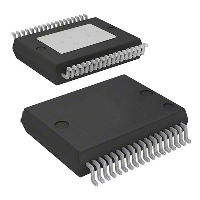


 工商网监
湘ICP备2023018690号
工商网监
湘ICP备2023018690号
