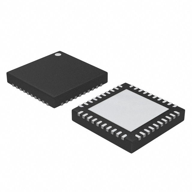
L99LD21
High power LED driver for automotive applications
Datasheet - production data
– Peak current control
– Constant VLED x TOFF architecture
4)1���/��[�
*$'*����������36
Features
• AEC-Q100 qualified
• General
– ST SPI communication v4.1
– 5.5 to 24 V Operating battery voltage range
– Load dump protected
– QFN40L 6x6 (wettable flanks) with
exposed pad
– Timeout watchdog and limp home function
– Low standby current
• Boost Section
– Fixed frequency architecture,
programmable by SPI
– Peak current mode control
– Dual phase operation supported
– Input current limitation
– Soft start
– Overvoltage protection (OVP)
– Short feedback failure protection
– Constant voltage control
This is information on a product in full production.
Applications
• Low Beam
• High beam
• Daytime running light
• Turn indicator
• Position light
• Side marker
• Fog light
Description
The L99LD21 is a flexible LED driver, which is
specifically designed for the control of two
independent high brightness LED strings for
automotive front lighting applications. It consists
of a high efficiency monolithic boost controller and
a dual buck converter.
• Buck section
– Integrated switching mosfets
– Lossless current sensing without need of
external components
– Very accurate LED current setting
programming inductor's peak current and
peak-to-peak current ripple
– Adjustable peak current by SPI
– Adjustable current ripple by SPI
– Integrated PWM generation unit with 10-bit
resolution and phase shift
July 2018
• Protection and diagnostic
– Battery under voltage
– Temperature warning (2 thresholds)
– Overtemperature shutdown
– LED voltage digital feedback through SPI
– Buck outputs short circuit and open load
protection
The boost controller integrates a high current gate
driver for an external n-channel mosfet. It delivers
a constant output voltage, up to 60 V, which
supplies the inputs of the two integrated or
external buck converters.
The boost controller of two devices can be
stacked, in order to operate in dual phase for high
power applications, with an interleaving pattern
for an improved input current ripple.
The buck converters integrate n-channel mosfet
which is driven by a bootstrap circuit.
DS11130 Rev 5
1/73
www.st.com
�Contents
L99LD21
Contents
1
Introduction . . . . . . . . . . . . . . . . . . . . . . . . . . . . . . . . . . . . . . . . . . . . . . . . 8
1.1
2
3
4
Boost controller . . . . . . . . . . . . . . . . . . . . . . . . . . . . . . . . . . . . . . . . . . . . 13
2.1
General description . . . . . . . . . . . . . . . . . . . . . . . . . . . . . . . . . . . . . . . . . 13
2.2
Frequency selection . . . . . . . . . . . . . . . . . . . . . . . . . . . . . . . . . . . . . . . . . 13
2.3
Output voltage setting . . . . . . . . . . . . . . . . . . . . . . . . . . . . . . . . . . . . . . . 13
2.4
Overvoltage protection . . . . . . . . . . . . . . . . . . . . . . . . . . . . . . . . . . . . . . . 13
2.5
Feedback failure protection . . . . . . . . . . . . . . . . . . . . . . . . . . . . . . . . . . . 14
2.6
Operation in dual phase interleaved mode . . . . . . . . . . . . . . . . . . . . . . . . 14
2.7
Soft start . . . . . . . . . . . . . . . . . . . . . . . . . . . . . . . . . . . . . . . . . . . . . . . . . . 16
2.8
Slope compensation . . . . . . . . . . . . . . . . . . . . . . . . . . . . . . . . . . . . . . . . . 16
2.9
Operation together with the buck converters . . . . . . . . . . . . . . . . . . . . . . 16
Buck converters . . . . . . . . . . . . . . . . . . . . . . . . . . . . . . . . . . . . . . . . . . . 18
3.1
General description . . . . . . . . . . . . . . . . . . . . . . . . . . . . . . . . . . . . . . . . . 18
3.2
Bootstrap circuit . . . . . . . . . . . . . . . . . . . . . . . . . . . . . . . . . . . . . . . . . . . . 18
3.3
Peak and average current setting . . . . . . . . . . . . . . . . . . . . . . . . . . . . . . 18
3.4
Buck converter’s blank time . . . . . . . . . . . . . . . . . . . . . . . . . . . . . . . . . . . 20
3.5
Buck converter’s start-up . . . . . . . . . . . . . . . . . . . . . . . . . . . . . . . . . . . . . 21
3.6
Switching frequency . . . . . . . . . . . . . . . . . . . . . . . . . . . . . . . . . . . . . . . . . 21
Functional description . . . . . . . . . . . . . . . . . . . . . . . . . . . . . . . . . . . . . . 22
4.1
4.2
2/73
Typical application . . . . . . . . . . . . . . . . . . . . . . . . . . . . . . . . . . . . . . . . . . . 9
Operating modes . . . . . . . . . . . . . . . . . . . . . . . . . . . . . . . . . . . . . . . . . . . 22
4.1.1
Standby mode . . . . . . . . . . . . . . . . . . . . . . . . . . . . . . . . . . . . . . . . . . . . 22
4.1.2
Pre-standby mode . . . . . . . . . . . . . . . . . . . . . . . . . . . . . . . . . . . . . . . . . 23
4.1.3
Reset mode . . . . . . . . . . . . . . . . . . . . . . . . . . . . . . . . . . . . . . . . . . . . . . 23
4.1.4
Limp home . . . . . . . . . . . . . . . . . . . . . . . . . . . . . . . . . . . . . . . . . . . . . . . 23
4.1.5
Active mode . . . . . . . . . . . . . . . . . . . . . . . . . . . . . . . . . . . . . . . . . . . . . . 24
Programmable functions . . . . . . . . . . . . . . . . . . . . . . . . . . . . . . . . . . . . . 25
4.2.1
Activation of the buck output . . . . . . . . . . . . . . . . . . . . . . . . . . . . . . . . . 25
4.2.2
PWM dimming . . . . . . . . . . . . . . . . . . . . . . . . . . . . . . . . . . . . . . . . . . . . 25
DS11130 Rev 5
�L99LD21
Contents
4.3
5
6
7
4.3.1
Temperature warning . . . . . . . . . . . . . . . . . . . . . . . . . . . . . . . . . . . . . . . 26
4.3.2
Overtemperature shutdown . . . . . . . . . . . . . . . . . . . . . . . . . . . . . . . . . . 27
4.3.3
VS under voltage lockout . . . . . . . . . . . . . . . . . . . . . . . . . . . . . . . . . . . . 27
4.3.4
Buck TON minimum operation . . . . . . . . . . . . . . . . . . . . . . . . . . . . . . . . 27
4.3.5
Buck output’s short circuit to GND . . . . . . . . . . . . . . . . . . . . . . . . . . . . . 27
4.3.6
Buck TON maximum operation . . . . . . . . . . . . . . . . . . . . . . . . . . . . . . . . 28
4.3.7
Buck Open Load detection . . . . . . . . . . . . . . . . . . . . . . . . . . . . . . . . . . 28
SPI functional description . . . . . . . . . . . . . . . . . . . . . . . . . . . . . . . . . . . 29
5.1
SPI protocol . . . . . . . . . . . . . . . . . . . . . . . . . . . . . . . . . . . . . . . . . . . . . . . 29
5.2
SPI communication . . . . . . . . . . . . . . . . . . . . . . . . . . . . . . . . . . . . . . . . . 29
5.3
Address mapping . . . . . . . . . . . . . . . . . . . . . . . . . . . . . . . . . . . . . . . . . . . 31
5.4
Registers description . . . . . . . . . . . . . . . . . . . . . . . . . . . . . . . . . . . . . . . . 33
5.4.1
Control Register description . . . . . . . . . . . . . . . . . . . . . . . . . . . . . . . . . 33
5.4.2
Status Register description . . . . . . . . . . . . . . . . . . . . . . . . . . . . . . . . . . 39
5.4.3
Customer test and trimming registers description . . . . . . . . . . . . . . . . . 45
5.4.4
Customer test and trimming procedure description . . . . . . . . . . . . . . . . 46
Electrical specifications . . . . . . . . . . . . . . . . . . . . . . . . . . . . . . . . . . . . . 51
6.1
Absolute maximum ratings . . . . . . . . . . . . . . . . . . . . . . . . . . . . . . . . . . . . 51
6.2
ESD protection . . . . . . . . . . . . . . . . . . . . . . . . . . . . . . . . . . . . . . . . . . . . . 52
6.3
Thermal characteristics . . . . . . . . . . . . . . . . . . . . . . . . . . . . . . . . . . . . . . 52
6.4
Electrical characteristics . . . . . . . . . . . . . . . . . . . . . . . . . . . . . . . . . . . . . . 53
6.4.1
Supply . . . . . . . . . . . . . . . . . . . . . . . . . . . . . . . . . . . . . . . . . . . . . . . . . . 53
6.4.2
Boost controller . . . . . . . . . . . . . . . . . . . . . . . . . . . . . . . . . . . . . . . . . . . 54
6.4.3
Buck . . . . . . . . . . . . . . . . . . . . . . . . . . . . . . . . . . . . . . . . . . . . . . . . . . . 56
6.4.4
SPI . . . . . . . . . . . . . . . . . . . . . . . . . . . . . . . . . . . . . . . . . . . . . . . . . . . . . 62
6.4.5
Direct input . . . . . . . . . . . . . . . . . . . . . . . . . . . . . . . . . . . . . . . . . . . . . . . 63
6.4.6
PWM dimming . . . . . . . . . . . . . . . . . . . . . . . . . . . . . . . . . . . . . . . . . . . . 64
6.4.7
Digital timings . . . . . . . . . . . . . . . . . . . . . . . . . . . . . . . . . . . . . . . . . . . . 65
Package and PCB thermal data . . . . . . . . . . . . . . . . . . . . . . . . . . . . . . . 66
7.1
8
Protections . . . . . . . . . . . . . . . . . . . . . . . . . . . . . . . . . . . . . . . . . . . . . . . . 26
QFN-40L 6x6 thermal data . . . . . . . . . . . . . . . . . . . . . . . . . . . . . . . . . . . . 66
Package information . . . . . . . . . . . . . . . . . . . . . . . . . . . . . . . . . . . . . . . . 67
DS11130 Rev 5
3/73
4
�Contents
L99LD21
8.1
9
QFN-40L 6x6 package information . . . . . . . . . . . . . . . . . . . . . . . . . . . . . 67
Order codes . . . . . . . . . . . . . . . . . . . . . . . . . . . . . . . . . . . . . . . . . . . . . . . 69
Appendix A Glossary . . . . . . . . . . . . . . . . . . . . . . . . . . . . . . . . . . . . . . . . . . . . . . . 70
Revision history . . . . . . . . . . . . . . . . . . . . . . . . . . . . . . . . . . . . . . . . . . . . . . . . . . . . 71
4/73
DS11130 Rev 5
�L99LD21
List of tables
List of tables
Table 1.
Table 2.
Table 3.
Table 4.
Table 5.
Table 6.
Table 7.
Table 8.
Table 9.
Table 10.
Table 11.
Table 12.
Table 13.
Table 14.
Table 15.
Table 16.
Table 17.
Table 18.
Table 19.
Table 20.
Table 21.
Table 22.
Table 23.
Table 24.
Table 25.
Table 26.
Table 27.
Table 28.
Table 29.
Table 30.
Table 31.
Table 32.
Table 33.
Table 34.
Table 35.
Table 36.
Table 37.
Table 38.
Table 39.
Table 40.
Table 41.
Table 42.
Table 43.
Table 44.
Table 45.
Table 46.
Table 47.
Table 48.
Pin functionality. . . . . . . . . . . . . . . . . . . . . . . . . . . . . . . . . . . . . . . . . . . . . . . . . . . . . . . . . . 11
Reference voltage configuration . . . . . . . . . . . . . . . . . . . . . . . . . . . . . . . . . . . . . . . . . . . . . 13
Operating modes . . . . . . . . . . . . . . . . . . . . . . . . . . . . . . . . . . . . . . . . . . . . . . . . . . . . . . . . 24
DIN pin Map for Buck1 and Buck2 . . . . . . . . . . . . . . . . . . . . . . . . . . . . . . . . . . . . . . . . . . . 25
Command byte (8 bit) . . . . . . . . . . . . . . . . . . . . . . . . . . . . . . . . . . . . . . . . . . . . . . . . . . . . . 29
Data byte 2 . . . . . . . . . . . . . . . . . . . . . . . . . . . . . . . . . . . . . . . . . . . . . . . . . . . . . . . . . . . . . 29
Data byte 1 . . . . . . . . . . . . . . . . . . . . . . . . . . . . . . . . . . . . . . . . . . . . . . . . . . . . . . . . . . . . . 29
Data byte 0 . . . . . . . . . . . . . . . . . . . . . . . . . . . . . . . . . . . . . . . . . . . . . . . . . . . . . . . . . . . . . 30
Operation code definition . . . . . . . . . . . . . . . . . . . . . . . . . . . . . . . . . . . . . . . . . . . . . . . . . . 30
Global Status Byte . . . . . . . . . . . . . . . . . . . . . . . . . . . . . . . . . . . . . . . . . . . . . . . . . . . . . . . 30
Global Status Byte description . . . . . . . . . . . . . . . . . . . . . . . . . . . . . . . . . . . . . . . . . . . . . . 31
RAM memory map . . . . . . . . . . . . . . . . . . . . . . . . . . . . . . . . . . . . . . . . . . . . . . . . . . . . . . . 31
ROM memory map . . . . . . . . . . . . . . . . . . . . . . . . . . . . . . . . . . . . . . . . . . . . . . . . . . . . . . . 32
CR#1: Control Register 1 . . . . . . . . . . . . . . . . . . . . . . . . . . . . . . . . . . . . . . . . . . . . . . . . . . 33
CR#2: Control Register 2 . . . . . . . . . . . . . . . . . . . . . . . . . . . . . . . . . . . . . . . . . . . . . . . . . . 34
CR#3: Control Register 3 . . . . . . . . . . . . . . . . . . . . . . . . . . . . . . . . . . . . . . . . . . . . . . . . . . 35
CR#4: Control Register 4 . . . . . . . . . . . . . . . . . . . . . . . . . . . . . . . . . . . . . . . . . . . . . . . . . . 36
Constant VLED x TOFF selection. . . . . . . . . . . . . . . . . . . . . . . . . . . . . . . . . . . . . . . . . . . . 37
DIN map table for Buck Cell X . . . . . . . . . . . . . . . . . . . . . . . . . . . . . . . . . . . . . . . . . . . . . . 37
Boost clock selection . . . . . . . . . . . . . . . . . . . . . . . . . . . . . . . . . . . . . . . . . . . . . . . . . . . . . 37
Buck input voltage window . . . . . . . . . . . . . . . . . . . . . . . . . . . . . . . . . . . . . . . . . . . . . . . . . 38
SR#1: Status Register 1 . . . . . . . . . . . . . . . . . . . . . . . . . . . . . . . . . . . . . . . . . . . . . . . . . . . 39
SR#2: Status Register 2 . . . . . . . . . . . . . . . . . . . . . . . . . . . . . . . . . . . . . . . . . . . . . . . . . . . 41
SR#3: Status Register 3 . . . . . . . . . . . . . . . . . . . . . . . . . . . . . . . . . . . . . . . . . . . . . . . . . . . 44
Watchdog status . . . . . . . . . . . . . . . . . . . . . . . . . . . . . . . . . . . . . . . . . . . . . . . . . . . . . . . . . 44
CT: Ctm Trimming Register . . . . . . . . . . . . . . . . . . . . . . . . . . . . . . . . . . . . . . . . . . . . . . . . 45
Writing test conditions. . . . . . . . . . . . . . . . . . . . . . . . . . . . . . . . . . . . . . . . . . . . . . . . . . . . . 46
Testing procedure description . . . . . . . . . . . . . . . . . . . . . . . . . . . . . . . . . . . . . . . . . . . . . . 48
Default peak current selection for Buck Cell 1 . . . . . . . . . . . . . . . . . . . . . . . . . . . . . . . . . . 50
Default VLEDxTOFF Selection for Buck Cell 1. . . . . . . . . . . . . . . . . . . . . . . . . . . . . . . . . . 50
Absolute maximum ratings . . . . . . . . . . . . . . . . . . . . . . . . . . . . . . . . . . . . . . . . . . . . . . . . . 51
ESD protection . . . . . . . . . . . . . . . . . . . . . . . . . . . . . . . . . . . . . . . . . . . . . . . . . . . . . . . . . . 52
QFN40L 6x6 thermal resistance . . . . . . . . . . . . . . . . . . . . . . . . . . . . . . . . . . . . . . . . . . . . . 52
Thermal characteristics. . . . . . . . . . . . . . . . . . . . . . . . . . . . . . . . . . . . . . . . . . . . . . . . . . . . 52
Supply . . . . . . . . . . . . . . . . . . . . . . . . . . . . . . . . . . . . . . . . . . . . . . . . . . . . . . . . . . . . . . . . . 53
Boost gate driver. . . . . . . . . . . . . . . . . . . . . . . . . . . . . . . . . . . . . . . . . . . . . . . . . . . . . . . . . 54
Boost controller . . . . . . . . . . . . . . . . . . . . . . . . . . . . . . . . . . . . . . . . . . . . . . . . . . . . . . . . . . 54
Boost controller reference voltage . . . . . . . . . . . . . . . . . . . . . . . . . . . . . . . . . . . . . . . . . . . 55
Buck converter power stage . . . . . . . . . . . . . . . . . . . . . . . . . . . . . . . . . . . . . . . . . . . . . . . . 56
Inductor peak current selection. . . . . . . . . . . . . . . . . . . . . . . . . . . . . . . . . . . . . . . . . . . . . . 58
VLEDxTOFF constants . . . . . . . . . . . . . . . . . . . . . . . . . . . . . . . . . . . . . . . . . . . . . . . . . . . . 61
SPI signal description . . . . . . . . . . . . . . . . . . . . . . . . . . . . . . . . . . . . . . . . . . . . . . . . . . . . . 62
SPI timings . . . . . . . . . . . . . . . . . . . . . . . . . . . . . . . . . . . . . . . . . . . . . . . . . . . . . . . . . . . . . 62
Direct Input pin limits . . . . . . . . . . . . . . . . . . . . . . . . . . . . . . . . . . . . . . . . . . . . . . . . . . . . . 63
PWMCLK and Fall back PWM description . . . . . . . . . . . . . . . . . . . . . . . . . . . . . . . . . . . . . 64
Digital timings description . . . . . . . . . . . . . . . . . . . . . . . . . . . . . . . . . . . . . . . . . . . . . . . . . . 65
PCB properties . . . . . . . . . . . . . . . . . . . . . . . . . . . . . . . . . . . . . . . . . . . . . . . . . . . . . . . . . . 66
QFN-40L 6x6 mechanical data . . . . . . . . . . . . . . . . . . . . . . . . . . . . . . . . . . . . . . . . . . . . . . 68
DS11130 Rev 5
5/73
6
�List of tables
Table 49.
Table 50.
Table 51.
6/73
L99LD21
Device summary . . . . . . . . . . . . . . . . . . . . . . . . . . . . . . . . . . . . . . . . . . . . . . . . . . . . . . . . . 69
Glossary . . . . . . . . . . . . . . . . . . . . . . . . . . . . . . . . . . . . . . . . . . . . . . . . . . . . . . . . . . . . . . . 70
Document revision history . . . . . . . . . . . . . . . . . . . . . . . . . . . . . . . . . . . . . . . . . . . . . . . . . 71
DS11130 Rev 5
�L99LD21
List of figures
List of figures
Figure 1.
Figure 2.
Figure 3.
Figure 4.
Figure 5.
Figure 6.
Figure 7.
Figure 8.
Figure 9.
Figure 10.
Figure 11.
Figure 12.
Figure 13.
Figure 14.
Figure 15.
Figure 16.
Functional block diagram . . . . . . . . . . . . . . . . . . . . . . . . . . . . . . . . . . . . . . . . . . . . . . . . . . . 9
Typical application schematic . . . . . . . . . . . . . . . . . . . . . . . . . . . . . . . . . . . . . . . . . . . . . . . 10
Application diagram . . . . . . . . . . . . . . . . . . . . . . . . . . . . . . . . . . . . . . . . . . . . . . . . . . . . . . 10
Connection diagram . . . . . . . . . . . . . . . . . . . . . . . . . . . . . . . . . . . . . . . . . . . . . . . . . . . . . . 11
Pin connections in dual-phase boost controller . . . . . . . . . . . . . . . . . . . . . . . . . . . . . . . . . 15
Slope compensation . . . . . . . . . . . . . . . . . . . . . . . . . . . . . . . . . . . . . . . . . . . . . . . . . . . . . . 16
Peak current control principle . . . . . . . . . . . . . . . . . . . . . . . . . . . . . . . . . . . . . . . . . . . . . . . 19
Inductor and mosfet current waveforms . . . . . . . . . . . . . . . . . . . . . . . . . . . . . . . . . . . . . . . 20
Device state diagram . . . . . . . . . . . . . . . . . . . . . . . . . . . . . . . . . . . . . . . . . . . . . . . . . . . . . 22
Testing flow chart . . . . . . . . . . . . . . . . . . . . . . . . . . . . . . . . . . . . . . . . . . . . . . . . . . . . . . . . 47
IL_PEAK vs DAC code - Low Rdson . . . . . . . . . . . . . . . . . . . . . . . . . . . . . . . . . . . . . . . . . . . . . . . . . . . . . 60
IL_PEAK vs DAC code - High Rdson . . . . . . . . . . . . . . . . . . . . . . . . . . . . . . . . . . . . . . . . . . . . . . . . . . . . . 60
VLED x TOFF vs DAC code . . . . . . . . . . . . . . . . . . . . . . . . . . . . . . . . . . . . . . . . . . . . . . . . . 61
PWM clock failure and reset sequence . . . . . . . . . . . . . . . . . . . . . . . . . . . . . . . . . . . . . . . 64
QFN-40L 6x6 on four-layers PCB . . . . . . . . . . . . . . . . . . . . . . . . . . . . . . . . . . . . . . . . . . . . 66
QFN-40L 6x6 package dimensions . . . . . . . . . . . . . . . . . . . . . . . . . . . . . . . . . . . . . . . . . . 67
DS11130 Rev 5
7/73
7
�Introduction
1
L99LD21
Introduction
The L99LD21 is a monolithic driver IC, which controls the current of two independent high
power LED strings, whose forward current and voltage can reach up to 1.5 A (average) and
up to 50V respectively.
This device has been designed with dedicated functions, in order to fulfill the stringent
requirements of automotive front lighting applications.
The device offers a high level of flexibility, without any change of the external components,
thanks to its programmability through the ST SPI interface. This feature support generic
platform approaches, which require a software configurability of several parameters. This
robust interface, offers a detailed diagnostic of the device itself, as well as of the controlled
LED strings.
As the device potentially controls safety critical functions such as low beams and turn
indicators, built-in features are integrated in order to support a high level of functional safety.
The L99LD21 features a timeout watchdog, a monitoring of the watchdog counter, a limp
home function and a direct input. The ST SPI protocol takes into account FMEA case.
The device consists of a boost controller, which controls the PWM of an external n-channel
mosfet and provides a stabilized voltage (VBOOST). The input of the boost stage must be
connected to the battery voltage through a reverse polarity protection.
The boost controllers of two L99LD21 can be combined to form a dual-phase, interleaved
boost controller. Special care has been taken for the current balancing between the different
phases and for the switching activity of the boost mosfets with 180° phase shift.
The output of the boost controller supplies the input of the two independent integrated buck
converters, or any other external buck converters, whose input voltage is compatible with
VBOOST. The integrated buck converters are based on constant off-time architecture (for a
given LED output voltage) and control the peak current and the peak-to-peak current ripple
of their respective inductors.
Operating in continuous conduction mode, the average of each LED string’s current, which
is connected to the output of each buck converter, is tightly controlled.
This architecture, which consists of cascaded boost and buck stages (see Figure 2), allows
the control of a wide range of LED strings, whose forward voltage is independent from the
battery voltage.
With the aim of ensuring a wide operating inductor current range, the Buck mosfets can be
set in low or high RDS_ON modes, so that two different inductor peak current (ILx_PEAK)
ranges [0.179 A ÷ 0.849 A] or [0.362 A ÷ 1.695 A] can be selected.
The average LED current is controlled by setting the inductor's peak current and peak-topeak current ripple. Sensing of the peak current is integrated, not requiring any external
shunt resistance, which saves cost and reduces the power dissipation.
Buck n-channel mosfet RDS_ON value depends on the operative conditions as junction
temperature, Input voltage and LED string current. For example, at VBuckin = 45 V,
Iled = 700 mA, Tj = 25 °C the maximum RDS_ON is 400 mΩ (low RDS_ON mode).
8/73
DS11130 Rev 5
�L99LD21
1.1
Introduction
Typical application
Figure 1. Functional block diagram
96
69�[�V@
��
��
��
��
��
��
��
�
�
�
�
�
�
�
�
�
�
�
��
��
��
��
��
��
'$&�FRGH
*$'*����������36
DS11130 Rev 5
61/73
72
�Electrical specifications
6.4.4
L99LD21
SPI
Table 42. SPI signal description
Symbol
CSN
SCK
SDI
Parameter
Test conditions
Note:
Typ
Max
High State
0.7 * V3V3
—
V3V3
Low State
—
—
0.3 * V3V3
High State
0.7 * V3V3
—
V3V3
Low State
—
—
0.3 * V3V3
High State
0.7 * V3V3
—
V3V3
Low State
—
—
0.3 * V3V3
Chip Select Not
Unit
V
Serial Clock
V
Serial data Input
V
Serial data Output - High State
IOUT = -1 mA
VSPI-0.5
VSPI-0.2
—
Serial data Output - Low State
IOUT = 1 mA
—
0.2
0.5
Output leakage current
—
-1
—
1
SDO
ILK
Min
V
µA
See also Chapter 5: SPI functional description.
Table 43. SPI timings
Symbol
Tsck
Parameter
Test conditions
Min
Typ
Max
Unit
Serial clock (SCK) period
250
ns
THsck
SCK high time
100
ns
TLsck
SCK low time
100
ns
Trise_in
CSN, SCK, SDI rise time
Fsck = 4 MHz
25
ns
Tfall_in
CSN, SCK, SDI fall time
Fsck = 4 MHz
25
ns
THcsn
CSN high time
TScsn
6
µs
CSN setup time, CSN low
before SCK rising
100
ns
TSsck
SCK setup time, SCK low
before CSN rising
100
ns
TSsdi
SDI setup time before SCK
rising
25
ns
SDI hold time
25
ns
Thold_sdi
62/73
Tcsn_v
CSN falling until SDO valid
Cout = 50 pF;
Iout = ±1 mA
100
ns
Tcsn_v
CSN rising until SDO tristate
Cout = 50 pF;
Iout = ±4 mA
100
ns
Tsck_v
SCK falling until SDO valid
Cout = 50 pF
60
ns
TRsdo
SDO rise time
Cout = 50 pF;
Iout = -1 mA
100
ns
DS11130 Rev 5
50
�L99LD21
Electrical specifications
Table 43. SPI timings (continued)
Symbol
TFsdo
Tcsn_low_t
6.4.5
Parameter
SDO fall time
Test conditions
Min
Typ
Max
Unit
50
100
ns
35
50
ms
Cout = 50 pF;
Iout = 1 mA
CSN low timeout
20
Direct input
Table 44. Direct Input pin limits
Symbol
Parameter
VDIN_L
DIN Low threshold
VDIN_H
DIN High threshold
Test conditions
Min
0.7 * V3V3
DS11130 Rev 5
Typ
Max
Unit
—
0.3 * V3V3
V
—
V3V3
V
63/73
72
�Electrical specifications
6.4.6
L99LD21
PWM dimming
..
Table 45. PWMCLK and Fall back PWM description
Symbol
Parameter
Test conditions
Min
Typ
Max
Unit
0.3 * V3V3
V
VPWMCLK_L
PWMCLK low threshold
VPWMCLK_H
PWMCLK high threshold
0.7 * V3V3
V3V3
V
FPWMCLK
PWMCLK input frequency
range
102400
409600
Hz
0
26500
Hz
210
KHz
FPWMCLK_FAIL
PWMCLK frequency fail
detection range
FFALLBACK_CLK
Fall back PWM frequency
clock
190
200
Figure 14. PWM clock failure and reset sequence
�
3:0�&ORFN�IURP�&
a�����N+]�
� 5HDG�DQG�&OHDU�
RI�3:0&/.�)DLO
'HWHFWLRQ�RI�
3:0&/.�)DLO
/��/'��B�
3:0B&/.
&RUUHFW�3:0&/.�
� VLJQDO�LV�GHWHFWHG
�
5HDG�DQG�&OHDU�
RI�3:0&/.�)DLO
([WHUQDO�3:0�&ORFN�VLJQDO�ORVW���
WKH�GHYLFH�XVHV�WKH�LQWHUQDO�
�IDOO�EDFN��FORFNa����N+]�
3:0�&ORFN�IURP�&
a�����N+]�
/��/'��B�
3:0B&/.
3:0�FORFN�FRXQWHU�
/��/'��B�
/��/'��B�
3:0B&/.
3:0�FORFN�FRXQWHU�
/��/'��B�
3:0�FORFN�FRXQWHU�
/��/'��B�
6\QFKURQL]HG�RU�
XQV\QFKURQL]HG�3:0�
GLPPLQJ�FORFN�FRXQWHUV
3:0�FORFN�FRXQWHU�IHG�
E\�LQWHUQDO�����N+]��IDOO�
EDFN��FORFN
7KH�3:0�FORFN�FRXQWHU�LV�
IHG�E\�WKH�H[WHUQDO�
3:0&/.�VLJQDO
3:0�FORFN�FRXQWHUV�IUR]HQ�
GXH�WR�PLVVLQJ�FORFN�VLJQDO
3:0&/.)DLO�ELW
�
�
$�3:0�&/.�)DLO�FRXQWHU�LV�LPSOHPHQWHG
,W�LV�LQFUHPHQWHG�LI�QR�ULVLQJ�HGJH�RQ�3:0&/.�SLQ�LV�
GHWHFWHG�ZLWKLQ����V
7KH�3:0�&/.�)DLO�FRXQWHU�LV�GHFUHPHQWHG�ZKHQ���ULVLQJ�
HGJHV�RQ�3:0&/.�SLQ�DUH�GHWHFWHG�ZLWKLQ����V
�
(YHQ�LI�WKH�3:0&/.�)DLO�FRXQWHU�LV�UHVHW��WKH�3:0&/.�
)DLO�ELW�LV�VWLOO�VHW�DQG�WKH�3:0�FORFN�FRXQWHU�IRU�WKH�ORZ�
IUHTXHQF\�3:0�GLPPLQJ�LV��VWLOO�IHG�E\�WKH�LQWHUQDO�3:0�
&ORFN��a����N+]�
$�3:0�&/.�)DLO�LV�UHSRUWHG�LI�WKH�FRXQWHU�UHDFKHV��
7KH�3:0�FORFN�FRXQWHU�IRU�WKH�ORZ�IUHTXHQF\�3:0�
GLPPLQJ�LV�IHG�E\�WKH�LQWHUQDO�3:0�&ORFN��a����N+]�
7KH�3:0&/.)DLO�ELW�LV�VHW
�
�
$�63,�5HDG�DQG�&OHDU�&RPPDQG�RI�WKH�
3:0&/.�)DLO�ELW�LV�GHWHFWHG
+RZHYHU��WKH�3:0�&/.�)DLO�FRXQWHU�LV�QRW�
UHVHW��WKHUHIRUH��WKLV�FRPPDQG�KDV�QR�HIIHFW
$�3:0�&/.�)DLO�FRXQWHU�UHVHW��GHFUHPHQWHG�GRZQ�WR�
]HUR��VLQFH�D�YDOLG�3:0&/.�VLJQDO�LV�GHWHFWHG�
�IUHTXHQF\�!����N+]��ULVLQJ�HGJHV�ZLWKLQ����V�
$�UHDG�DQG�FOHDU�FRPPDQG�RI�WKH�3:0&/.�)DLO�ELW�LV�
GHWHFWHG�ZKLOH�WKH�3:0&/.�)DLO�FRXQWHU�LV�UHVHW�
7KH�3:0&/.�FRXQWHUV�DUH�UHVHW�DQG�DUH�IHG�E\�WKH�
VLJQDO�RQ�WKHLU�3:0&/.�SLQ�
*$3*����������&)7
64/73
DS11130 Rev 5
�L99LD21
6.4.7
Electrical specifications
Digital timings
Table 46. Digital timings description
Symbol
Min
Typ
Max
Unit
Watchdog timeout
period
45
50
55
ms
tCSN_TIMEOUT
CSN timeout
90
115
140
ms
tAUTORESTART
Autorestart time in limp
home mode
45
50
55
ms
tWD
tVS,UV
tDIN_FT(1)
Parameter
VS undervoltage filter
time
32
µs
DIN Filter time
32
µs
12.8
µs
tDIN_ST
DIN status information
time
tSKEW
Timing skew for DIN
tVSPI_FT
VSPI Filtering Time
tWAKE_UP
Time for a complete
wake up (V3V3 >
VPOR_L)
tSTDBY
tOVT
tBST_OVP
tBST_OVP_RST
tBOOST_FB_FAIL
Test conditions
2.5
µs
32
µs
190
µs
DIN low
Time needed for a
Cap on V3V3 = 4.7 µF
transition to standby
mode (V3V3 < VPOR_L) V3V3 < 2.5 V
1.6
ms
Filtering time for
overtemperature (OVT
bit will be set if Tj >
TTSD for more than
tOVT)
1.2
µs
BST_OVP flag set
filtering time
32
µs
BST_OVP flag reset
filtering time
10
ms
BST_FB_FAIL flag set
filtering time
1.6
µs
CSN low or DIN high for
t > tWAKEUP
Cap on V3V3 = 4.7 µF
V3V3 > 3 V
guaranteed by
frequency oscillator
(20 MHz typical) and
scan
1. Digital timings guaranteed by scan. WD and autorestart timings limits added to give indication on application cases.
DS11130 Rev 5
65/73
72
�Package and PCB thermal data
L99LD21
7
Package and PCB thermal data
7.1
QFN-40L 6x6 thermal data
Figure 15. QFN-40L 6x6 on four-layers PCB
Table 47. PCB properties
Dimension
66/73
Value
Board finish thickness
1.6 mm +/- 10%
Board dimension
129 mm x 60 mm
Board Material
FR4
Copper thickness (outer layers)
0.070 mm
Copper thickness (inner layers)
0.035 mm
Thermal vias separation
1.2 mm
Thermal via diameter
0.3 mm +/- 0.08 mm
Copper thickness on vias
0.025 mm
DS11130 Rev 5
�L99LD21
8
Package information
Package information
In order to meet environmental requirements, ST offers these devices in different grades of
ECOPACK® packages, depending on their level of environmental compliance. ECOPACK®
specifications, grade definitions and product status are available at: www.st.com.
ECOPACK® is an ST trademark.
8.1
QFN-40L 6x6 package information
Figure 16. QFN-40L
6x6 package dimensions
("1(����������$'5
DS11130 Rev 5
67/73
72
�Package information
L99LD21
Table 48. QFN-40L 6x6 mechanical data
Symbol
Min
Typ
Max
A
0.85
0.95
1.05
A1
0
A3
0.20
b
0.20
0.25
0.30
D
5.85
6.00
6.15
E
5.85
6.00
6.15
D2
3.95
4.10
4.25
E2
3.95
4.10
4.25
e
0.50
J
0.45
L
68/73
0.05
0.40
0.50
L1
0.20
L2
0.05
L3
0.20
L4
0.075
P
0.31
P1
0.18
P2
0.18
ddd
0.08
DS11130 Rev 5
0.60
�L99LD21
9
Order codes
Order codes
Table 49. Device summary
Order code
Package
QFN-40L 6x6
Tube
Tape and reel
L99LD21Q6
L99LD21Q6TR
DS11130 Rev 5
69/73
72
�Glossary
L99LD21
Appendix A
Glossary
Table 50. Glossary
Acronym
µC
Microcontroller
ADC
Analog / Digital converter
ASSP
Application Specific Standard Product
CPHA
Clock Phase
CPOL
Clock Polarity
CSN
Chip select not (normal low) (SPI)
CTRL
Control register
FE
Functional Error
FS
Fail Safe
GE
Device Error
GSB
GSBN
70/73
Description
Global Status Byte
Global Status Bit Not
GW
Global Warning
I/O
Input /Output pins
DIN
Direct input
LH
Limp Home
LSB
Least Significant Bit
MCU
Mirocontroller
SDI
SPI Data Input (slave)
SDO
SPI Data Onput (slave)
MSB
Most Significant Bit
DS11130 Rev 5
�L99LD21
Revision history
Revision history
Table 51. Document revision history
Date
Revision
03-Jul-2015
1
Initial release.
2
Updated Features and Description
Updated following sections:
– Chapter 1: Introduction
– Section 1.1: Typical application
– Section 2.3: Output voltage setting
– Section 2.4: Overvoltage protection
Added Section 2.5: Feedback failure protection
Updated following sections:
– Section 2.6: Operation in dual phase interleaved mode
– Section 2.7: Soft start
– Section 2.8: Slope compensation
– Section 2.9: Operation together with the buck converters
– Section 3.1: General description
– Section 3.3: Peak and average current setting
– Section 3.4: Buck converter’s blank time
– Section 3.5: Buck converter’s start-up
– Section 3.6: Switching frequency
– Section 4.1: Operating modes
– Section 4.1.4: Limp home
– Section 4.2.2: PWM dimming
– Section 4.3.1: Temperature warning
– Section 4.3.2: Overtemperature shutdown
Added following sections:
– Section 4.3.4: Buck TON minimum operation
– Section 4.3.6: Buck TON maximum operation
– Section 4.3.7: Buck Open Load detection
Removed “Open load” section
Updated following sections:
– Chapter 5: SPI functional description
– Section 6.1: Absolute maximum ratings
– Chapter 6.3: Thermal characteristics
– Chapter 6.4: Electrical characteristics
Added Chapter 7: Package and PCB thermal data
Added Section 8.1: QFN-40L 6x6 package information
Updated Chapter 9: Order codes
28-Sep-2015
Changes
DS11130 Rev 5
71/73
72
�Revision history
L99LD21
Table 51. Document revision history (continued)
Date
72/73
Revision
Changes
13-Mar-2018
3
Datasheet status promoted from preliminary data to production data.
Removed in cover page the image of the TQFP-48 package.
Updated:
– Features and description in cover page;
– Section 1: Introduction on page 8;
– Figure 1: Functional block diagram on page 9;
– Figure 2: Typical application schematic on page 10
– added Figure 3: Application diagram on page 10;
– removed TQFP48 connection diagram;
– removed column “TQFP48” on Table 1: Pin functionality;
– Section 2.5: Feedback failure protection;
– Section 2.7: Soft start;
– Section 3.1: General description on page 18;
– Section 3.3: Peak and average current setting
– Section 4.1.1: Standby mode;
– Section 4.1.2: Pre-standby mode;
– Section 4.2.2: PWM dimming
– Table 13: ROM memory map;
– Section 5.4.1: Control Register description;
– Section 5.4.2: Status Register description;
– Section 5.4.3: Customer test and trimming registers description;
– Section 5.4.4: Customer test and trimming procedure description;
– Section 6: Electrical specifications
– removed “TQFP-48L thermal data” in Section 7: Package and
PCB thermal data;
– removed “TQFP-48L package information” in Section 8: Package
information;
– removed reference to TQFP48 package in Section 9: Order
codes.
10-May-2018
4
Updated equation in Section 2.3: Output voltage setting. Updated
Table 37.
25-Jul-2018
5
Updated Figure 9: Device state diagram.
DS11130 Rev 5
�L99LD21
IMPORTANT NOTICE – PLEASE READ CAREFULLY
STMicroelectronics NV and its subsidiaries (“ST”) reserve the right to make changes, corrections, enhancements, modifications, and
improvements to ST products and/or to this document at any time without notice. Purchasers should obtain the latest relevant information on
ST products before placing orders. ST products are sold pursuant to ST’s terms and conditions of sale in place at the time of order
acknowledgement.
Purchasers are solely responsible for the choice, selection, and use of ST products and ST assumes no liability for application assistance or
the design of Purchasers’ products.
No license, express or implied, to any intellectual property right is granted by ST herein.
Resale of ST products with provisions different from the information set forth herein shall void any warranty granted by ST for such product.
ST and the ST logo are trademarks of ST. All other product or service names are the property of their respective owners.
Information in this document supersedes and replaces information previously supplied in any prior versions of this document.
© 2018 STMicroelectronics – All rights reserved
DocID028061 Rev 4
73/73
73
�