LD29300
3 A, very low drop voltage regulator
Datasheet - production data
Table 1. Device summary
Order codes
Output voltages
LD29300P2MTR
ADJ
P²PAK
Features
Very low dropout voltage (typ. 0.4 V at 3 A)
High accuracy: ±1% @ 25°C
Guaranteed output current up to 3 A
Internal current and thermal limit
Logic controlled electronic shutdown
Description
The LD29300 is a high current, high accuracy,
low-dropout voltage regulator. This regulator
features 400 mV dropout voltage and very low
ground current. Designed for high current loads,
this device is also used in lower current,
extremely low dropout-critical systems, where its
tiny dropout voltage and ground current values
are important attributes. Typical applications are
in power supply switching post regulation, series
power supply for monitors, series power supply
for VCRs and TVs, computer systems and
battery-powered systems.
August 2017
This is information on a product in full production.
DocID9248 Rev 15
1/17
www.st.com
�Contents
LD29300
Contents
1
Diagram . . . . . . . . . . . . . . . . . . . . . . . . . . . . . . . . . . . . . . . . . . . . . . . . . . . 3
2
Pin configuration . . . . . . . . . . . . . . . . . . . . . . . . . . . . . . . . . . . . . . . . . . . . 4
3
Typical application . . . . . . . . . . . . . . . . . . . . . . . . . . . . . . . . . . . . . . . . . . 5
4
Maximum ratings . . . . . . . . . . . . . . . . . . . . . . . . . . . . . . . . . . . . . . . . . . . . 6
5
Electrical characteristics . . . . . . . . . . . . . . . . . . . . . . . . . . . . . . . . . . . . . 7
6
Typical characteristics . . . . . . . . . . . . . . . . . . . . . . . . . . . . . . . . . . . . . . . 8
7
Package information . . . . . . . . . . . . . . . . . . . . . . . . . . . . . . . . . . . . . . . . 11
7.1
8
Packaging information . . . . . . . . . . . . . . . . . . . . . . . . . . . . . . . . . . . . . . 14
8.1
9
2/17
P2PAK package information . . . . . . . . . . . . . . . . . . . . . . . . . . . . . . . . . . . 11
P2PAK packaging information . . . . . . . . . . . . . . . . . . . . . . . . . . . . . . . . . 14
Revision history . . . . . . . . . . . . . . . . . . . . . . . . . . . . . . . . . . . . . . . . . . . 16
DocID9248 Rev 15
�LD29300
1
Diagram
Diagram
Figure 1. Schematic diagram
DocID9248 Rev 15
3/17
17
�Pin configuration
2
LD29300
Pin configuration
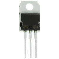
Figure 2. Pin connections (top view)
P2PAK
4/17
DocID9248 Rev 15
�LD29300
3
Typical application
Typical application
Figure 3. Application circuit
VO = VREF (1 + R1/R2)
DocID9248 Rev 15
5/17
17
�Maximum ratings
4
LD29300
Maximum ratings
Table 2. Absolute maximum ratings
Symbol
Parameter
Value
Unit
30 (1)
V
VI
DC input voltage
IO
Output current
Internally limited
mA
PD
Power dissipation
Internally limited
mW
TSTG
Storage temperature range
- 55 to 150
°C
TOP
Operating junction temperature range
- 40 to 125
°C
1. Above 14 V the device is automatically in shutdown.
Note:
Absolute maximum ratings are those values beyond which damage to the device may occur.
Functional operation under these conditions is not implied.
Table 3. Thermal data
Symbol
6/17
Parameter
P²PAK
Unit
RthJA
Thermal resistance junction-ambient
60
°C/W
RthJC
Thermal resistance junction-case
3
°C/W
DocID9248 Rev 15
�LD29300
5
Electrical characteristics
Electrical characteristics
IO = 10 mA, TJ = 25 °C, VI = 3.23 V, VINH = 2 V, CI = 330 nF, CO = 10 μF adjust pin tied to
output pin.
Table 4. Electrical characteristics of LD29300#ADJ
Symbol
Parameter
Test conditions
Min.
Typ.
Max.
Unit
Minimum operating input
voltage
IO = 10 mA to 3 A, TJ = -40 to 125°C
VO
Load regulation
IO = 10 mA to 3 A
0.2
1.0
%
VO
Line regulation
VI = 2.5 V to 13 V
0.06
0.5
%
VREF
Reference voltage
IO = 10 mA to 3 A, VI = 2.5 to 4.5 V
TJ = -40 to 125°C (1)
1.23
+1%
SVR
Supply voltage rejection
f = 120 Hz, VI = 3.23 1 V, IO = 1.5A (2)
VI
Iq
IADJ
Isc
VIL
Quiescent current
-1%
V
-2%
65
+2%
75
V
dB
IO = 1.5 A, TJ = -40 to 125°C
20
50
IO = 3 A, TJ = -40 to 125°C
45
100
VI = 13 V, VINH = GND, TJ = -40 to 125°C
130
180
μA
1
μA
Adjust pin current
TJ = -40 to 125°C
Short circuit current
VI - VO = 5.5 V
Control input logic low
2.5
OFF MODE
4.5
(1),T
J
(1),
= -40 to 125°C
TJ = -40 to 125°C
A
0.8
VIH
Control input logic high
ON MODE
IINH
Control input current
TJ = -40 to 125°C, VINH = 13 V
5
eN
Output noise voltage
BP = 10 Hz to 100 kHz, IO = 100 mA(2)
50
mA
2
V
V
10
μA
μVRMS
1. Reference voltage is measured between output and GND pin, with ADJ PIN tied to VOUT.
2. Guaranteed by design.
DocID9248 Rev 15
7/17
17
�Typical characteristics
6
LD29300
Typical characteristics
Figure 4. Output voltage vs. temperature
Figure 5. Dropout voltage vs. temperature
Figure 6. Dropout voltage vs. output current
Figure 7. Quiescent current vs. output current
(VI = 13 V)
8/17
DocID9248 Rev 15
�LD29300
Typical characteristics
Figure 8. Quiescent current vs. output current
(VI = 4.5 V)
Figure 9. Quiescent current vs. supply voltage
Figure 10. Quiescent current vs. temperature
(IO = 100 mA)
Figure 11. Quiescent current vs. temperature
(IO = 3 A)
Figure 12. Short circuit current vs. temperature
Figure 13. Supply voltage rejection vs.
temperature
DocID9248 Rev 15
9/17
17
�Typical characteristics
LD29300
Figure 14. Stability vs. CO
Figure 15. Line transient
VI = 3.5 to 5.5 V, ILOAD = 10 mA, VO = 2.5 V, CO = 10 μF
Figure 16. Load transient
VI = 4.5 V, IO = 10 mA to 3 A, VO = 2.5 V, CO = 47 μF
10/17
DocID9248 Rev 15
�LD29300
7
Package information
Package information
In order to meet environmental requirements, ST offers these devices in different grades of
ECOPACK® packages, depending on their level of environmental compliance. ECOPACK®
specifications, grade definitions and product status are available at: www.st.com.
ECOPACK® is an ST trademark.
7.1
P2PAK package information
Table 5. P2PAK mechanical data
mm
Dim.
Min.
Typ.
Max.
A
4.30
4.80
A2
0.03
0.23
C
1.17
1.37
D
2.40
2.80
D1
8.95
9.35
E
0.45
0.60
F
0.80
1.05
G
3.20
3.60
G1
6.60
7.00
H1
8.5
H2
10.00
L
15
L1
10.40
15.85
8
L2
1.27
1.40
M
2.4
3.2
R
V2
0.40
0°
DocID9248 Rev 15
8°
11/17
17
�Package information
LD29300
Figure 17. P2PAK outline
�������@$
12/17
DocID9248 Rev 15
�LD29300
Package information
Figure 18. P2PAK footprint
�������@$
DocID9248 Rev 15
13/17
17
�Packaging information
LD29300
8
Packaging information
8.1
P2PAK packaging information
Table 6. P2PAK tape and reel mechanical data
mm
Dim.
Min.
Typ.
A
180
C
12.8
D
20.2
N
60
13
T
14/17
Max.
13.2
14.4
Ao
10.50
10.6
10.70
Bo
15.70
15.80
15.90
Ko
4.80
4.90
5.00
Po
3.9
4.0
4.1
P
11.9
12.0
12.1
DocID9248 Rev 15
�LD29300
Packaging information
Figure 19. P2PAK tape and reel dimensions
DocID9248 Rev 15
15/17
17
�Revision history
9
LD29300
Revision history
Table 7. Document revision history
Date
Revision
21-Oct-2005
7
Order codes updated.
10-Apr-2007
8
Order codes updated.
11-May-2007
9
Order codes updated.
08-Jun-2007
10
Order codes updated.
03-Apr-2008
11
Modified: Table 1 on page 1.
11-Jul-2008
12
Modified: Table 1 on page 1.
13-Sep-2012
13
Updated: Table 1 on page 1.
14
Part numbers LD29300XX, LD29300XX18 and LD29300XX33 have
been changed to LD29300.
Updated the Description in cover page and Table 1: Device
summary.
Updated Table 3: Thermal data, Section 5: Electrical characteristics
and Section 7: Package mechanical data.
Added Section 8: Packaging mechanical data.
Minor text changes.
15
Removed version of device with fixed output voltage (updated
Features, Table 1: Device summary, removed schematic and
electrical characteristics, updated Figure 2: Pin connections (top
view), Figure 3: Application circuit)
Minor textual updates
18-Nov-2013
30-Aug-2017
16/17
Changes
DocID9248 Rev 15
�LD29300
IMPORTANT NOTICE – PLEASE READ CAREFULLY
STMicroelectronics NV and its subsidiaries (“ST”) reserve the right to make changes, corrections, enhancements, modifications, and
improvements to ST products and/or to this document at any time without notice. Purchasers should obtain the latest relevant information on
ST products before placing orders. ST products are sold pursuant to ST’s terms and conditions of sale in place at the time of order
acknowledgement.
Purchasers are solely responsible for the choice, selection, and use of ST products and ST assumes no liability for application assistance or
the design of Purchasers’ products.
No license, express or implied, to any intellectual property right is granted by ST herein.
Resale of ST products with provisions different from the information set forth herein shall void any warranty granted by ST for such product.
ST and the ST logo are trademarks of ST. All other product or service names are the property of their respective owners.
Information in this document supersedes and replaces information previously supplied in any prior versions of this document.
© 2017 STMicroelectronics – All rights reserved
DocID9248 Rev 15
17/17
17
�


 工商网监
湘ICP备2023018690号
工商网监
湘ICP备2023018690号
