LD2985
Very low drop and low noise voltage regulator with inhibit function
Datasheet - production data
Description
SOT23-5L
Features
• Very low dropout voltage (280 mV at 150 mA
and 7 mV at 1 mA load)
• Very low quiescent current (2 mA typ. at 150
mA load and 80 µA at no load)
• Output current up to 150 mA
The LD2985 is a 150 mA fixed output voltage
regulator. The ultra low drop voltage and the low
quiescent current make them particularly suitable
for low noise, low power applications, and in
battery powered systems. In sleep mode
quiescent current is less than 1 µA when INHIBIT
pin is pulled low. Shutdown logic control function
is available on pin 3 (TTL compatible). This
means that when the device is used as local
regulator, it is possible to put a part of the board in
standby, decreasing the total power consumption.
An external capacitor, CBYP = 10 nF, connected
between bypass pin and GND reduces the noise
to 30 µVrms. Typical application are in cellular
phone, palmtop laptop computer, personal digital
assistant (PDA), personal stereo, camcorder and
camera.
• Logic controlled electronic shutdown
Table 1. Device summary
• Output voltage of 1.8, 2.5, 2.8, 3, 3.1, 3.3, 5 V
Order codes
Output voltages
• Low output noise voltage 30 µVrms
LD2985BM18R
1.8 V
• Small package SOT23-5L
LD2985BM25R
2.5 V
• Temperature range: - 40 °C to 125 °C
LD2985BM28R
2.8 V
LD2985BM30R
3.0 V
LD2985BM31R
3.1 V
LD2985BM33R
3.3 V
LD2985BM50R
5.0 V
• Internal current and thermal limit
August 2021
This is information on a product in full production.
DocID8189 Rev 16
1/18
www.st.com
18
�Contents
LD2985
Contents
1
Diagram . . . . . . . . . . . . . . . . . . . . . . . . . . . . . . . . . . . . . . . . . . . . . . . . . . . 3
2
Pin configuration . . . . . . . . . . . . . . . . . . . . . . . . . . . . . . . . . . . . . . . . . . . . 4
3
Maximum ratings . . . . . . . . . . . . . . . . . . . . . . . . . . . . . . . . . . . . . . . . . . . . 5
4
Electrical characteristics . . . . . . . . . . . . . . . . . . . . . . . . . . . . . . . . . . . . . 6
5
Typical characteristics . . . . . . . . . . . . . . . . . . . . . . . . . . . . . . . . . . . . . . . 8
6
Application notes . . . . . . . . . . . . . . . . . . . . . . . . . . . . . . . . . . . . . . . . . . 11
6.1
External capacitors . . . . . . . . . . . . . . . . . . . . . . . . . . . . . . . . . . . . . . . . . . .11
6.2
Input capacitor . . . . . . . . . . . . . . . . . . . . . . . . . . . . . . . . . . . . . . . . . . . . . .11
6.3
Output capacitor . . . . . . . . . . . . . . . . . . . . . . . . . . . . . . . . . . . . . . . . . . . . .11
6.4
Important . . . . . . . . . . . . . . . . . . . . . . . . . . . . . . . . . . . . . . . . . . . . . . . . . .11
6.5
Inhibit input operation . . . . . . . . . . . . . . . . . . . . . . . . . . . . . . . . . . . . . . . . .11
6.6
Reverse current . . . . . . . . . . . . . . . . . . . . . . . . . . . . . . . . . . . . . . . . . . . . 12
7
Package information . . . . . . . . . . . . . . . . . . . . . . . . . . . . . . . . . . . . . . . . 13
8
Packing information . . . . . . . . . . . . . . . . . . . . . . . . . . . . . . . . . . . . . . . . 15
9
Revision history . . . . . . . . . . . . . . . . . . . . . . . . . . . . . . . . . . . . . . . . . . . 17
2/18
DocID8189 Rev 16
�LD2985
1
Diagram
Diagram
Figure 1. Schematic diagram
DocID8189 Rev 16
3/18
�Pin configuration
2
LD2985
Pin configuration
Figure 2. Pin connections (top view)
4
5
1
2
3
SC12360
Table 2. Pin description
Pin n°
Symbol
Name and function
1
IN
2
GND
3
INHIBIT
Control switch ON/OFF. Inhibit is not internally pulled-up; it cannot be left
floating. Disable the device when connected to GND or to a positive
voltage less than 0.18 V
4
Bypass
Bypass pin: capacitor to be connected to GND in order to improve the
thermal noise performance
5
OUT
Input port
Ground pin
Output port
Table 3. Thermal data
Symbol
4/18
Parameter
Value
Unit
RthJC
Thermal resistance junction-case
81
°C/W
RthJA
Thermal resistance junction-ambient
255
°C/W
DocID8189 Rev 16
�LD2985
3
Maximum ratings
Maximum ratings
Table 4. Absolute maximum ratings
Symbol
VI
VINH
Note:
Parameter
Value
Unit
DC input voltage
-0.3 to 16
V
INHIBIT input voltage
-0.3 to 16
V
IO
Output current
Internally limited
PD
Power dissipation
Internally limited
TSTG
Storage temperature range
-65 to 150
°C
TOP
Operating junction temperature range
-40 to 125
°C
Absolute maximum ratings are those values beyond which damage to the device may occur.
Functional operation under these condition is not implied.
DocID8189 Rev 16
5/18
�Electrical characteristics
4
LD2985
Electrical characteristics
TJ = 25 °C, VI = VO + 1 V, IO = 50 mA, VINH= 2 V, CI = CO = 1 µF, unless otherwise specified.
Table 5. Electrical characteristics
Symbol
VOP
VO
VO
VO
VO
VO
Parameter
Operating input voltage
Output voltage
Output voltage
Output voltage
Output voltage
Output voltage
Output voltage
VO
Load regulation
VO
ISC
Test conditions
Output voltage
Short-circuit current
6/18
Line regulation
Typ.
2.5
1.8
Max.
Unit
16
V
VI = 2.8 V
1.755
IO = 1 to 150 mA
1.746
1.854
IO = 1 to 150 mA, TJ= -40 to 125 °C
1.728
1.872
VI = 3.5 V
2.437
IO = 1 to 150 mA
2.425
2.575
IO = 1 to 150 mA, TJ= -40 to 125 °C
2.4
2.6
VI = 3.8 V
2.73
IO = 1 to 150 mA
2.716
2.884
IO = 1 to 150 mA, TJ= -40 to 125 °C
2.688
2.912
VI = 4.0 V
2.925
IO = 1 to 150 mA
2.91
3.09
IO = 1 to 150 mA, TJ= -40 to 125 °C
2.88
3.12
VI = 4.1 V
3.023
IO = 1 to 150 mA
3.007
3.193
IO = 1 to 150 mA, TJ= -40 to 125 °C
2.976
3.224
VI = 4.3 V
3.218
IO = 1 to 150 mA
3.201
3.399
IO = 1 to 150 mA, TJ= -40 to 125 °C
3.168
3.432
2.5
2.8
3.0
3.1
3.3
IO = 1 to 150 mA, TJ= -40 to 125 °C
1.845
5.15
IO = 1 to 150 mA, TJ= -40 to 125 °C
4.8
5.2
V
mV
5.125
400
DocID8189 Rev 16
V
3.382
4.85
VI = VO + 1 V to 16 V, IO = 1 mA,
TJ= -40 to 125 °C
V
3.177
IO = 1 to 150 mA
0.003
V
3.075
4.875
RL = 0
V
2.87
20
5
V
2.562
VI = 6.0 V
VI = VO + 1 V to 16 V, IO = 1 mA
ΔVO/ΔVI
Min.
V
mA
0.014
0.032
%/VI
�LD2985
Electrical characteristics
Table 5. Electrical characteristics (continued)
Symbol
Parameter
Test conditions
Min.
IO = 0
Typ.
Max.
1
3
IO = 0, TJ= -40 to 125 °C
5
IO = 1 mA
7
IO = 1 mA, TJ= -40 to 125 °C
VDROP
Dropout voltage
IO = 10 mA
40
mV
120
IO = 50 mA, TJ= -40 to 125 °C
280
IO = 150 mA, TJ= -40 to 125 °C
80
IO = 0, TJ= -40 to 125 °C
100
IO = 1 mA, TJ= -40 to 125 °C
200
IO = 10 mA, TJ= -40 to 125 °C
µA
600
IO = 50 mA, TJ= -40 to 125 °C
2000
IO = 150 mA, TJ= -40 to 125 °C
0
VINH
很抱歉,暂时无法提供与“LD2985BM285R”相匹配的价格&库存,您可以联系我们找货
免费人工找货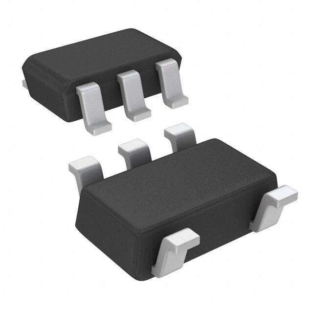


 工商网监
湘ICP备2023018690号
工商网监
湘ICP备2023018690号
