LD39030SJ28R

LD39030SJ28R

  • 厂商:

    STMICROELECTRONICS(意法半导体)

  • 封装:

    UFBGA4

  • 描述:

    IC REG LIN 2.8V 300MA 4FLIPCHIP

  • 详情介绍
  • 数据手册
  • 价格&库存
LD39030SJ28R 数据手册
LD39030SJ 300 mA low quiescent current soft-start, low noise voltage regulator Datasheet - production data Applications • Mobile phones • Personal digital assistants (PDAs) • Cordless phones and similar battery-powered systems • Digital still cameras. Description Flip-chip 4 Features • Input voltage from 1.5 to 5.5 V • Ultra low dropout voltage (200 mV typ. at 300 mA load) • Very low quiescent current (20 μA typ. at no load, 40 μA typ. at 300 mA load, 1 μA max. in off mode) • Very low noise (30 μVRMS from 1 kHz to 100 kHz at VOUT = 1.8 V) The LD39030SJ is a low noise voltage regulator that provides 300 mA maximum current from an input voltage in the 1.5 V to 5.5 V range, with a typical dropout voltage of 200 mV. It is stabilized with a ceramic capacitor on the output. The ultra low drop voltage, low quiescent current, and low noise features make it suitable for low power battery-powered applications. Power supply rejection is typically 62 dB at low frequencies and starts to roll off at 10 kHz. An enable logic control function puts the LD39030SJ in shutdown mode allowing a total current consumption lower than 1 μA. The device also includes a short-circuit constant current limiting and thermal protection. • Output voltage tolerance: ± 2.0 % @ 25 °C Table 1. Device summary • 300 mA guaranteed output current Order codes Output voltages • Wide range of output voltages available on request: 0.8 V to 4.5 V with 100 mV step LD39030SJ10R 1V • Logic-controlled electronic shutdown LD39030SJ12R 1.2 V • Compatible with ceramic capacitor COUT = 1 μF LD39030SJ126R 1.26 V • Internal current and thermal limit LD39030SJ28R 2.8 V • Flip-chip 4 bumps 0.8 x 0.8 mm pitch 0.4 mm LD39030SJ285R 2.85 V • Internal soft-start (typ. 100 μs) LD39030SJ33R 3.3 V • Temperature range: - 40 °C to 125 °C February 2014 This is information on a product in full production. DocID18103 Rev 5 1/18 www.st.com Contents LD39030SJ Contents 1 Block diagram . . . . . . . . . . . . . . . . . . . . . . . . . . . . . . . . . . . . . . . . . . . . . . 3 2 Pin configuration . . . . . . . . . . . . . . . . . . . . . . . . . . . . . . . . . . . . . . . . . . . . 4 3 Typical application . . . . . . . . . . . . . . . . . . . . . . . . . . . . . . . . . . . . . . . . . . 5 4 Maximum ratings . . . . . . . . . . . . . . . . . . . . . . . . . . . . . . . . . . . . . . . . . . . . 6 5 Electrical characteristics . . . . . . . . . . . . . . . . . . . . . . . . . . . . . . . . . . . . . 7 6 Soft-start function . . . . . . . . . . . . . . . . . . . . . . . . . . . . . . . . . . . . . . . . . . . 9 7 Typical performance characteristics . . . . . . . . . . . . . . . . . . . . . . . . . . . 10 8 Package mechanical data . . . . . . . . . . . . . . . . . . . . . . . . . . . . . . . . . . . . 13 9 Packaging mechanical data . . . . . . . . . . . . . . . . . . . . . . . . . . . . . . . . . . 15 10 Revision history . . . . . . . . . . . . . . . . . . . . . . . . . . . . . . . . . . . . . . . . . . . 17 2/18 DocID18103 Rev 5 LD39030SJ 1 Block diagram Block diagram Figure 1. Block diagram OUT IN BandGap 1.22 V R1 Trimming Thermal Protection R2 Enable EN GND DocID18103 Rev 5 3/18 18 Pin configuration 2 LD39030SJ Pin configuration Figure 2. Pin connection (top view) Table 2. Pin description 4/18 Pin n° Symbol A2 EN A1 GND B2 IN B1 OUT Function Enable pin logic input: low = shutdown, high = active Common ground Input voltage of the LDO Output voltage DocID18103 Rev 5 LD39030SJ 3 Typical application Typical application Figure 3. Typical application circuit VIN IN 1 μF VEN VOUT OUT 1 μF EN Load GND DocID18103 Rev 5 5/18 18 Maximum ratings 4 LD39030SJ Maximum ratings Table 3. Absolute maximum ratings Symbol VIN Parameter DC input voltage Value Unit - 0.3 to 6 V VOUT DC output voltage - 0.3 to VIN + 0.3 V VEN Enable input voltage - 0.3 to VIN + 0.3 V IOUT Output current Internally limited mA Power dissipation Internally limited mW PD TSTG Storage temperature range - 65 to 150 °C TOP Operating junction temperature range - 40 to 125 °C Note: Absolute maximum ratings are those values beyond which damage to the device may occur. Functional operation under these conditions is not implied. All values are referred to GND. Table 4. Thermal data Symbol RthJA 6/18 Parameter Thermal resistance junction-ambient DocID18103 Rev 5 Value Unit 180 °C/W LD39030SJ 5 Electrical characteristics Electrical characteristics TJ = 25 °C, VIN = VOUT(NOM) + 1 V, CIN = COUT = 1 μF, IOUT = 1 mA, VEN = VIN, unless otherwise specified. Table 5. Electrical characteristics Symbol Parameter VIN Operating input voltage Test conditions (1) Min. Typ. 1.5 Turn-on threshold 1.45 Max. Unit 5.5 V 1.48 V VUVLO Turn-off threshold VOUT VOUT accuracy 1.30 1.35 VOUT >1.5 V, IOUT=1 mA, TJ=25 °C -2.0 2.0 % VOUT >1.5 V, IOUT=1 mA, -40 °C
LD39030SJ28R
物料型号:LD39030SJ

器件简介:LD39030SJ是一款低噪声电压调节器,提供最大300 mA的电流,输入电压范围在1.5 V至5.5 V,典型下拉电压为200 mV。它使用陶瓷电容在输出端进行稳定。超低下拉电压、低静态电流和低噪声特性使其非常适合低功耗电池供电应用。

引脚分配:该器件有4个引脚,包括使能引脚EN、地GND、输入电压IN和输出电压OUT。

参数特性: - 工作输入电压:1.5 V至5.5 V - 超低下拉电压:200 mV(典型值,300 mA负载时) - 非常低的静态电流:20 μA(典型值,无负载时),40 μA(典型值,300 mA负载时),最大1 μA的关闭模式 - 非常低的噪声:在1 kHz至100 kHz时为30 μVRMS(当VOUT = 1.8 V) - 输出电压容差:±2.0 % - 保证的输出电流:300 mA - 可应要求提供广泛的输出电压范围:0.8 V至4.5 V,步进为100 mV - 逻辑控制的电子关闭功能 - 与1 μF陶瓷电容兼容 - 内部电流和热限制 - 内部软启动(典型值100 μs) - 温度范围:-40 °C至125 °C

功能详解:LD39030SJ具有内部软启动电路,可以在不需要任何外部软启动电容的情况下,将启动时间增加到100 μs,从而将调节器的涌入电流减少到原始值的1/3。

应用信息:适用于移动电话、个人数字助理(PDAs)、无绳电话和类似的电池供电系统、数字静止相机等。

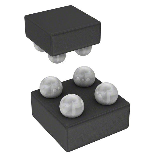
封装信息:采用4个焊点的倒装芯片封装,尺寸为0.8 x 0.8 mm,节距为0.4 mm。
LD39030SJ28R 价格&库存

很抱歉,暂时无法提供与“LD39030SJ28R”相匹配的价格&库存,您可以联系我们找货

免费人工找货