LDS3985 SERIES
ULTRA LOW DROP-LOW NOISE BICMOS 300mA V.REG. FOR USE WITH VERY LOW ESR OUTPUT CAPACITOR
s s
s
s
s
s
s
s
s s
s s
INPUT VOLTAGE FROM 2.5V TO 6V STABLE WITH LOW ESR CERAMIC CAPACITORS ULTRA LOW DROPOUT VOLTAGE (150mV TYP. AT 300mA LOAD, 0.4mV TYP. AT 1mA LOAD) VERY LOW QUIESCENT CURRENT (85µA TYP. AT NO LOAD, 200µA TYP. AT 300mA LOAD; MAX 1.5µA IN OFF MODE) GUARANTEED OUTPUT CURRENT UP TO 300mA WIDE RANGE OF OUTPUT VOLTAGE: 1.25V; 1.35; 1.5V; 1.8V; 2V; 2.1V; 2.2V; 2.5V; 2.6V; 2.7V; 2.8V; 2.85V; 2.9V; 3V; 3.1V; 3.2V; 3.3V; 4.7V FAST TURN-ON TIME: TYP. 240µs [CO=2.2µF, CBYP= 33nF AND IO=1mA] LOGIC-CONTROLLED ELECTRONIC SHUTDOWN INTERNAL CURRENT AND THERMAL LIMIT OUTPUT LOW NOISE VOLTAGE 30µVRMS OVER 10Hz to 100KHz S.V.R. OF 55dB AT 1KHz, 50dB AT 10KHz TEMPERATURE RANGE: -40°C TO 125°C
DFN6
SOT23-5L
It is stable with ceramic and high quality tantalum capacitor. The ultra low drop-voltage, low quiescent current and low noise makes it suitable for low power applications and in battery powered systems. Regulator ground current increases only slightly in dropout, further prolonging the battery life. Shutdown Logic Control function is available, this means that when the device is used as local regulator, it is possible to put a part of the board in standby, decreasing the total power consumption. Typical applications are in mobile phone and similar battery powered wireless systems, portable information appliances.
DESCRIPTION The LDS3985 provides up to 300mA, from 2.5V to 6V input voltage. Figure 1: Schematic Diagram
December 2004
Rev. 1
1/13
�LDS3985 SERIES
Table 1: Absolute Maximum Ratings
Symbol VI VO VINH IO PD TSTG TOP DC Input Voltage DC Output Voltage INHIBIT Input Voltage Output Current Power Dissipation Storage Temperature Range Operating Junction Temperature Range Parameter Value -0.3 to 6 (*) -0.3 to VI+0.3 -0.3 to VI+0.3 Internally limited Internally limited -65 to 150 -40 to 125 °C °C Unit V V V
Absolute Maximum Ratings are those values beyond which damage to the device may occur. Functional operation under these condition is not implied. (*) The input pin is able to withstand non repetitive spike of 6.5V for 200ms.
Table 2: Thermal Data
Symbol Parameter SOT23-5L 81 255 DFN6 10 55 Unit °C/W °C/W
Rthj-case Thermal Resistance Junction-case Rthj-amb Thermal Resistance Junction-ambient
Table 3: Order Codes
SOT23-5L LDS3985M125R (*) LDS3985M135R (*) LDS3985M15R (*) LDS3985M18R LDS3985M20R (*) LDS3985M21R (*) LDS3985M22R (*) LDS3985M25R LDS3985M26R (*) LDS3985M27R (*) LDS3985M28R LDS3985M285R (*) LDS3985M29R LDS3985M30R (*) LDS3985M31R (*) LDS3985M32R (*) LDS3985M33R LDS3985M47R (*) LDS3985M48R (*) LDS3985M49R (*) LDS3985M50R (*)
(*) Available on request.
DFN6 LDS3985PM12R (*) LDS3985PM13R (*) LDS3985PM15R (*) LDS3985PM18R LDS3985PM20R (*) LDS3985PM21R (*) LDS3985PM22R (*) LDS3985PM25R LDS3985PM26R (*) LDS3985PM27R (*) LDS3985PM28R LDS3985PM285R (*) LDS3985PM29R (*) LDS3985PM30R (*) LDS3985PM31R (*) LDS3985PM32R (*) LDS3985PM33R LDS3985PM47R (*) LDS3985PM48R (*) LDS3985PM49R (*) LDS3985PM50R (*)
OUTPUT VOLTAGES 1.25 V 1.35 V 1.5 V 1.8 V 2.0 V 2.1 V 2.2 V 2.5 V 2.6 V 2.7 V 2.8 V 2.85 V 2.9 V 3.0 V 3.1 V 3.2 V 3.3 V 4.7 V 4.8 V 4.9 V 5.0 V
2/13
�LDS3985 SERIES
Figure 2: Connection Diagram (top view for SOT, top through view for DFN6)
SOT23-5L
DFN6
Table 4: Pin Description
Pin N° SOT23-5L 1 2 3 4 5 Pin N° DFN6 1 5 6 4 3 2 Symbol VI GND VINH BYPASS VO N.C. Input Voltage of the LDO Common Ground Inhibit Input Voltage: ON MODE when VINH ≥ 1.2V, OFF MODE when VINH ≤ 0.4V (Do not leave floating, not internally pulled down/up) Bypass Pin: Connect an external capacitor (usually 10nF) to minimize noise voltage Output Voltage of the LDO Not Connect. Name and Function
Figure 3: Typical Application Circuit
3/13
�LDS3985 SERIES
Table 5: Electrical Characteristics For LDS3985 (Tj = 25°C, VI = VO(NOM) +0.5V, CI = 1µF, C O = 2.2µF CBYP = 33nF, IO = 1mA, VINH = 1.4V, unless otherwise specified)
Symbol VI VO VO ∆VO ∆VO ∆VO ∆VO IQ Parameter Operating Input Voltage Output Voltage < 2.5V Output Voltage ≥ 2.5V Line Regulation (Note 1) Load Regulation Load Regulation IO = 1 mA TJ= -40 to 125°C IO = 1 mA TJ= -40 to 125°C VI = VO(NOM) + 0.5 to 6 VTJ= -40 to 125°C VO = 4.7 to 5V IO = 1 mA to 300mA TJ= -40 to 125°C IO = 1 mA to 300mA TJ= -40 to 125°C VO ≤ 2.5V VO ≥ 2.5V Test Conditions Min. 2.5 -50 -75 -2 -3 -0.1 -0.19 0.005 0.0008 5 85 150 200 TJ= -40 to 125°C 0.003 TJ= -40 to 125°C VDROP Dropout Voltage (Note 3) IO = 1mA IO = 1mA IO = 150mA IO = 150mA IO = 300mA IO = 300mA ISC SVR Short Circuit Current Supply Voltage Rejection RL = 0 f = 1KHz VI = VO(NOM)+0.25V ± VRIPPLE = 0.1V, IO= 50mA f = 10KHz For VO(NOM) < 2.5V, VI=2.55V VO ≥ VO(NOM) - 5% VI = 2.5V to 6V VINH = 0.4V CBYP = 33 nF Note 5 Capacitance (Note 6) ESR 2.2 5 TJ= -40 to 125°C 1.4 VI = 6V CO = 2.2 µF ±1 30 240 160 22 5000 nA µVRMS µs °C µF mΩ BW = 10 Hz to 100 KHz 300 TJ= -40 to 125°C 600 55 50 550 0.4 TJ= -40 to 125°C 150 250 mA dB TJ= -40 to 125°C 60 100 0.4 2 1.5 mV 300 Typ. Max. 6 50 75 2 3 0.1 0.19 0.01 0.004 %/mA %/mA mVPP µA % of VO(NOM) %/V Unit V mV
Output AC Line Regulation VI = VO(NOM) + 1 V, IO = 300mA, (Note 2) tR= tF = 30µs IO = 0 Quiescent Current ON MODE: VINH = 1.24V TJ= -40 to 125°C IO = 0 IO = 0 to 300mA IO = 0 to 300mA OFF MODE: VINH = 0.4V
IO(PK) VINH IINH eN tON TSHDN CO
Peak Output Current Inhibit Input Logic Low Inhibit Input Logic High Inhibit Input Current Output Noise Voltage Turn On Time (Note 4) Thermal Shutdown Output Capacitor
mA V
Note 1: For VO(NOM) < 2V VI = 2.5V Note 2: For VO(NOM) =1.25V VI = 2.5V Note 3: Dropout voltage is the input-to-output voltage difference at which the output voltage is 100mV below its nominal value. This specification does not apply for input voltages below 2.5V. Note 4: Turn -on time is time measured between the enable input just exceeding VINH High Value and the output voltage just reaching 95% of its nominal value Note 5: Typical thermal protection hysteresis is 20°C
4/13
�LDS3985 SERIES
TYPICAL PERFORMANCE CHARACTERISTICS (Tj = 25°C, VI = VO(NOM) +0.5V, CI = 1µF, CO = 2,2µF, CBYP = 33nF, IO = 1mA, VINH = 1.4V, unless otherwise specified) Figure 4: Output Voltage vs Temperature Figure 7: Shutdown Voltage vs Temperature
Figure 5: Output Voltage vs Temperature
Figure 8: Shutdown Voltage vs Temperature
Figure 6: Output Voltage vs Temperature
Figure 9: Line Regulation vs Temperature
5/13
�LDS3985 SERIES
Figure 10: Line Regulation vs Temperature Figure 13: Quiescent Current vs Temperature
Figure 11: Line Regulation vs Temperature
Figure 14: Quiescent Current vs Temperature
Figure 12: Quiescent Current vs Temperature
Figure 15: Supply Voltage Rejection vs Frequency
6/13
�LDS3985 SERIES
Figure 16: Dropout Voltage vs Temperature Figure 18: Inhibit Transient
VI = 5V, IO = 1mA, VINH = 0 to 1.2V, CI = CO = 1µF (cer), CBYP = 10nF, TR = TF = 1µs
Figure 17: Dropout Voltage vs Output Current
7/13
�LDS3985 SERIES
SOT23-5L MECHANICAL DATA
mm. DIM. MIN. A A1 A2 b C D E e H L 2.60 0.10 0.90 0.00 0.90 0.35 0.09 2.80 1.50 0.95 3.00 0.60 102.3 3.9 TYP MAX. 1.45 0.10 1.30 0.50 0.20 3.00 1.75 MIN. 35.4 0.0 35.4 13.7 3.5 110.2 59.0 37.4 118.1 23.6 TYP. MAX. 57.1 3.9 51.2 19.7 7.8 118.1 68.8 mils
.
7049676C
8/13
�LDS3985 SERIES
DFN6 (3x3) MECHANICAL DATA
mm. DIM. MIN. A A1 A2 A3 b D D2 E E2 e L L1 L2 K 0.20 0.20 0.24 0.13 7.9 0.33 2.90 1.92 2.90 1.11 0.95 0.45 7.9 9.4 5.1 3.00 3.00 0.80 0 0.65 0.20 0.43 3.10 2.12 3.10 1.31 13.0 114.2 75.6 114.2 43.7 37.4 17.7 118.1 118.1 TYP MAX. 1.00 0.05 0.75 MIN. 31.5 0.0 25.6 7.9 16.9 122.0 83.5 122.0 51.6 TYP. MAX. 39.4 2.0 29.5 inch
7387339A
9/13
�LDS3985 SERIES
Tape & Reel SOT23-xL MECHANICAL DATA
mm. DIM. MIN. A C D N T Ao Bo Ko Po P 3.13 3.07 1.27 3.9 3.9 3.23 3.17 1.37 4.0 4.0 12.8 20.2 60 14.4 3.33 3.27 1.47 4.1 4.1 0.123 0.120 0.050 0.153 0.153 0.127 0.124 0.054 0.157 0.157 13.0 TYP MAX. 180 13.2 0.504 0.795 2.362 0.567 0.131 0.128 0.0.58 0.161 0.161 0.512 MIN. TYP. MAX. 7.086 0.519 inch
10/13
�LDS3985 SERIES
Tape & Reel QFNxx/DFNxx (3x3) MECHANICAL DATA
mm. DIM. MIN. A C D N T Ao Bo Ko Po P 3.3 3.3 1.1 4 8 12.8 20.2 60 18.4 0.130 0.130 0.043 0.157 0.315 TYP MAX. 330 13.2 0.504 0.795 2.362 0.724 MIN. TYP. MAX. 12.992 0.519 inch
11/13
�LDS3985 SERIES
Table 6: Revision History
Date 02-Dic-2004 Revision 1 First Release. Description of Changes
12/13
�LDS3985 SERIES
Information furnished is believed to be accurate and reliable. However, STMicroelectronics assumes no responsibility for the consequences of use of such information nor for any infringement of patents or other rights of third parties which may result from its use. No license is granted by implication or otherwise under any patent or patent rights of STMicroelectronics. Specifications mentioned in this publication are subject to change without notice. This publication supersedes and replaces all information previously supplied. STMicroelectronics products are not authorized for use as critical components in life support devices or systems without express written approval of STMicroelectronics. The ST logo is a registered trademark of STMicroelectronics All other names are the property of their respective owners © 2004 STMicroelectronics - All Rights Reserved STMicroelectronics group of companies Australia - Belgium - Brazil - Canada - China - Czech Republic - Finland - France - Germany - Hong Kong - India - Israel - Italy - Japan Malaysia - Malta - Morocco - Singapore - Spain - Sweden - Switzerland - United Kingdom - United States of America www.st.com
13/13
�
很抱歉,暂时无法提供与“LDS3985M15R”相匹配的价格&库存,您可以联系我们找货
免费人工找货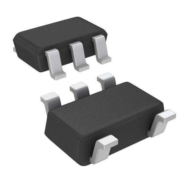


 工商网监
湘ICP备2023018690号
工商网监
湘ICP备2023018690号
