LED2472G
24-channels LED driver with error detection and gain control
Datasheet - production data
Description
74)3���(3
0/34���(3��[�
Features
• 24 constant current output channels
• Output current: from 4 mA to 72 mA
• 8 x 3 independently controlled channels (RGB)
• Current programmable through external
resistor
• 7-bit global current gain adjustment in two
ranges
• Error detection mode (both open and shorted
LED)
• Programmable shorted LED detection
thresholds
• Auto power-saving / auto wakeup
• Gradual output delay (selectable)
The LED2472G is a monolithic, low voltage, low
current power 24-bit shift register designed for
LED panel displays with particular features
oriented to indoor and outdoor LED screen
billboards. The LED2472G guarantees 20 V of
output driving capability, allowing several LEDs to
be connected in series. The device is configured
in 3 groups (red, green and blue) of 8
independently-controlled channels. The LED
current can be separately regulated for each color
within the range from 4 mA to 72 mA. This range
is divided into two sub-ranges and the current can
be adjusted within each range in 64 steps of
resolution (6 bits per color). A single external
resistor is required. All the controls and the shift
register data are accessible via serial interface. A
single 24-bit configuration register is used to
choose features and settings to fit the application.
The LED failure detection circuit checks 3
different conditions that can occur at the output
line: short to GND, short to LED power supply rail
or open channel. The auto power shutdown and
auto power-on feature (selectable) allows the
device to save power without any external
intervention. Thermal management includes
overtemperature flag and the output thermal
shutdown (170 °C). The high clock frequency of
up to 30 MHz makes the device suitable for high
data rate transmission. A selectable gradual
output delay reduces the inrush current. The
supply voltage ranges from 3 V and 5.5 V.
• Supply voltage: 3 V to 5.5 V
• Thermal shutdown and thermal flag
Table 1. Device summary
• Up to 30 MHz CLK 4 wires interface
• 20 V current generators rated voltage
Applications
Order code
Package
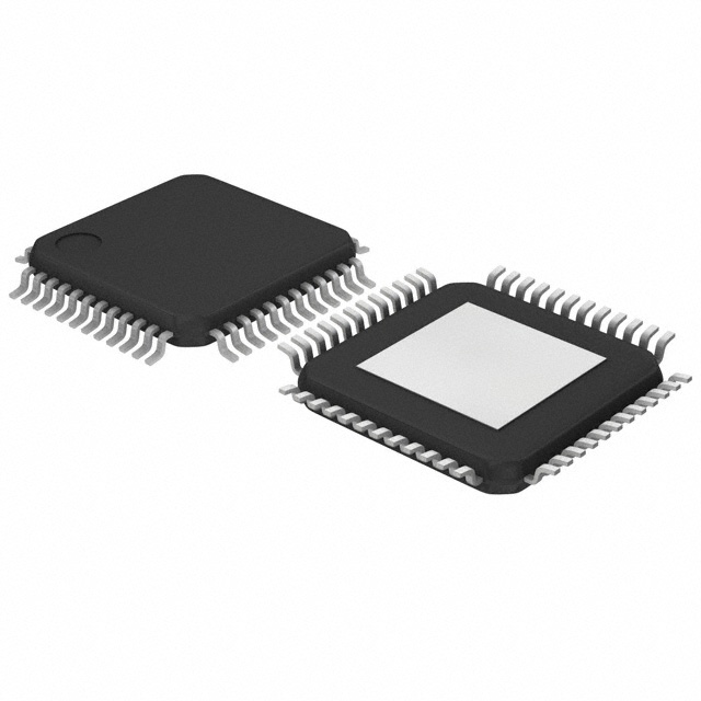
LED2472GBTR
TQFP48-EP
LED2472GQTR
MLPQ40-EP 5x5
Packaging
Tape and reel
• Full color large displays
• LED signage
• LED screens for indoor and outdoor billboards
July 2021
This is information on a product in full production.
DocID024620 Rev 5
1/39
www.st.com
39
�Contents
LED2472G
Contents
1
Pin description . . . . . . . . . . . . . . . . . . . . . . . . . . . . . . . . . . . . . . . . . . . . . 6
2
Absolute maximum ratings . . . . . . . . . . . . . . . . . . . . . . . . . . . . . . . . . . . 9
3
Thermal characteristics . . . . . . . . . . . . . . . . . . . . . . . . . . . . . . . . . . . . . 10
4
Electrical characteristics . . . . . . . . . . . . . . . . . . . . . . . . . . . . . . . . . . . . 11
4.1
Typical application circuit . . . . . . . . . . . . . . . . . . . . . . . . . . . . . . . . . . . . . 13
5
Switching characteristics . . . . . . . . . . . . . . . . . . . . . . . . . . . . . . . . . . . . 14
6
Timing . . . . . . . . . . . . . . . . . . . . . . . . . . . . . . . . . . . . . . . . . . . . . . . . . . . . 15
7
Simplified Internal block diagram . . . . . . . . . . . . . . . . . . . . . . . . . . . . . 16
7.1
8
Equivalent circuits of inputs and outputs . . . . . . . . . . . . . . . . . . . . . . . . . 17
Digital blocks . . . . . . . . . . . . . . . . . . . . . . . . . . . . . . . . . . . . . . . . . . . . . . 18
8.1
Register access . . . . . . . . . . . . . . . . . . . . . . . . . . . . . . . . . . . . . . . . . . . . 18
8.2
Configuration register . . . . . . . . . . . . . . . . . . . . . . . . . . . . . . . . . . . . . . . . 20
8.3
Current ranges (CFG 0-CFG 2) . . . . . . . . . . . . . . . . . . . . . . . . . . . . . . . . 21
8.4
Error detection conditions (CFG 3-CFG 5) . . . . . . . . . . . . . . . . . . . . . . . . 21
8.5
Auto power shutdown / wakeup (CFG 6) . . . . . . . . . . . . . . . . . . . . . . . . . 21
8.6
SDO delay (CFG 7) . . . . . . . . . . . . . . . . . . . . . . . . . . . . . . . . . . . . . . . . . 22
8.7
Gradual output delay (CFG 8) . . . . . . . . . . . . . . . . . . . . . . . . . . . . . . . . . 22
8.8
Data flow management (CFG 9-CFG 11) . . . . . . . . . . . . . . . . . . . . . . . . . 23
8.9
Gain register . . . . . . . . . . . . . . . . . . . . . . . . . . . . . . . . . . . . . . . . . . . . . . . 24
9
Current adjustment . . . . . . . . . . . . . . . . . . . . . . . . . . . . . . . . . . . . . . . . . 26
10
LED error detection . . . . . . . . . . . . . . . . . . . . . . . . . . . . . . . . . . . . . . . . . 28
11
Thermal shutdown and thermal alert . . . . . . . . . . . . . . . . . . . . . . . . . . 30
2/39
DocID024620 Rev 5
�LED2472G
Contents
12
Dropout voltage . . . . . . . . . . . . . . . . . . . . . . . . . . . . . . . . . . . . . . . . . . . . 31
13
Package mechanical data . . . . . . . . . . . . . . . . . . . . . . . . . . . . . . . . . . . . 32
14
Revision history . . . . . . . . . . . . . . . . . . . . . . . . . . . . . . . . . . . . . . . . . . . 38
DocID024620 Rev 5
3/39
�List of tables
LED2472G
List of tables
Table 1.
Table 2.
Table 3.
Table 4.
Table 5.
Table 6.
Table 7.
Table 8.
Table 9.
Table 10.
Table 11.
Table 12.
Table 13.
Table 14.
Table 15.
Table 16.
Table 17.
4/39
Device summary . . . . . . . . . . . . . . . . . . . . . . . . . . . . . . . . . . . . . . . . . . . . . . . . . . . . . . . . . . 1
Pin description . . . . . . . . . . . . . . . . . . . . . . . . . . . . . . . . . . . . . . . . . . . . . . . . . . . . . . . . . . . 7
Absolute maximum ratings . . . . . . . . . . . . . . . . . . . . . . . . . . . . . . . . . . . . . . . . . . . . . . . . . . 9
Thermal characteristics. . . . . . . . . . . . . . . . . . . . . . . . . . . . . . . . . . . . . . . . . . . . . . . . . . . . 10
Electrical characteristics . . . . . . . . . . . . . . . . . . . . . . . . . . . . . . . . . . . . . . . . . . . . . . . . . . . 11
Switching characteristics . . . . . . . . . . . . . . . . . . . . . . . . . . . . . . . . . . . . . . . . . . . . . . . . . . 14
Digital keys summary . . . . . . . . . . . . . . . . . . . . . . . . . . . . . . . . . . . . . . . . . . . . . . . . . . . . . 19
Configuration register . . . . . . . . . . . . . . . . . . . . . . . . . . . . . . . . . . . . . . . . . . . . . . . . . . . . . 20
Diagnostic thresholds . . . . . . . . . . . . . . . . . . . . . . . . . . . . . . . . . . . . . . . . . . . . . . . . . . . . . 21
Gradual output delay values . . . . . . . . . . . . . . . . . . . . . . . . . . . . . . . . . . . . . . . . . . . . . . . . 23
Gain register . . . . . . . . . . . . . . . . . . . . . . . . . . . . . . . . . . . . . . . . . . . . . . . . . . . . . . . . . . . . 24
Current adjustment example. . . . . . . . . . . . . . . . . . . . . . . . . . . . . . . . . . . . . . . . . . . . . . . . 27
Thermal alert status summary . . . . . . . . . . . . . . . . . . . . . . . . . . . . . . . . . . . . . . . . . . . . . . 30
Minimum dropout voltage for some current values (only one channel ON) . . . . . . . . . . . . 31
TQFP48-EP mechanical data . . . . . . . . . . . . . . . . . . . . . . . . . . . . . . . . . . . . . . . . . . . . . . . 33
MLPQ40-EP 5x5 mechanical data . . . . . . . . . . . . . . . . . . . . . . . . . . . . . . . . . . . . . . . . . . . 36
Document revision history . . . . . . . . . . . . . . . . . . . . . . . . . . . . . . . . . . . . . . . . . . . . . . . . . 38
DocID024620 Rev 5
�LED2472G
List of figures
List of figures
Figure 1.
Figure 2.
Figure 3.
Figure 4.
Figure 5.
Figure 6.
Figure 7.
Figure 8.
Figure 9.
Figure 10.
Figure 11.
Figure 12.
Figure 13.
Figure 14.
Figure 15.
Figure 16.
Figure 17.
Figure 18.
Figure 19.
Figure 20.
Figure 21.
Figure 22.
Pinout for TQFP48EP (top view) . . . . . . . . . . . . . . . . . . . . . . . . . . . . . . . . . . . . . . . . . . . . . 6
Pinout for MLPQ40 (top view). . . . . . . . . . . . . . . . . . . . . . . . . . . . . . . . . . . . . . . . . . . . . . . . 6
Typical application circuit . . . . . . . . . . . . . . . . . . . . . . . . . . . . . . . . . . . . . . . . . . . . . . . . . . 13
Timing for clock, serial-in, serial-out, latch enable and outputs . . . . . . . . . . . . . . . . . . . . . 15
OE and Outputs timing . . . . . . . . . . . . . . . . . . . . . . . . . . . . . . . . . . . . . . . . . . . . . . . . . . . . 15
LED2472G simplified block diagram. . . . . . . . . . . . . . . . . . . . . . . . . . . . . . . . . . . . . . . . . . 16
Input terminals . . . . . . . . . . . . . . . . . . . . . . . . . . . . . . . . . . . . . . . . . . . . . . . . . . . . . . . . . . 17
Data input time diagram . . . . . . . . . . . . . . . . . . . . . . . . . . . . . . . . . . . . . . . . . . . . . . . . . . . 18
Digital key timing diagram. . . . . . . . . . . . . . . . . . . . . . . . . . . . . . . . . . . . . . . . . . . . . . . . . . 19
Configuration register . . . . . . . . . . . . . . . . . . . . . . . . . . . . . . . . . . . . . . . . . . . . . . . . . . . . . 20
SDO Delay . . . . . . . . . . . . . . . . . . . . . . . . . . . . . . . . . . . . . . . . . . . . . . . . . . . . . . . . . . . . . 22
Gradual delay on first four channels of RED color group . . . . . . . . . . . . . . . . . . . . . . . . . 23
Different color sequence in data loading . . . . . . . . . . . . . . . . . . . . . . . . . . . . . . . . . . . . . . 24
Iout vs. gain . . . . . . . . . . . . . . . . . . . . . . . . . . . . . . . . . . . . . . . . . . . . . . . . . . . . . . . . . . . . 25
External resistor to connect to ISET pin . . . . . . . . . . . . . . . . . . . . . . . . . . . . . . . . . . . . . . 26
Error detection process. . . . . . . . . . . . . . . . . . . . . . . . . . . . . . . . . . . . . . . . . . . . . . . . . . . . 29
LE high for 14 CLK . . . . . . . . . . . . . . . . . . . . . . . . . . . . . . . . . . . . . . . . . . . . . . . . . . . . . . . 30
Typical dropout voltage vs. output current (only one channel ON) . . . . . . . . . . . . . . . . . . . 31
TQFP48-EP package dimensions . . . . . . . . . . . . . . . . . . . . . . . . . . . . . . . . . . . . . . . . . . . 32
TQFP48-EP recommended footprint . . . . . . . . . . . . . . . . . . . . . . . . . . . . . . . . . . . . . . . . . 34
MLPQ40-EP 5x5 package dimensions . . . . . . . . . . . . . . . . . . . . . . . . . . . . . . . . . . . . . . . . 35
MLPQ40-EP 5x5 recommended footprint . . . . . . . . . . . . . . . . . . . . . . . . . . . . . . . . . . . . . 37
DocID024620 Rev 5
5/39
�Pin description
1
LED2472G
Pin description
5�
*�
%�
5�
*�
%�
5�
*�
%�
5�
*�
%�
Figure 1. Pinout for TQFP48EP (top view)
��
��
��
��
��
��
��
��
��
��
��
��
1&
�
��
1&
6',
�
��
6'2
/(
�
��
52(
&/.
�
��
*2(
1&
�
��
%2(
1&
�
��
9''
1&
�
��
*1'
74)3���H[SRVHG�SDG
1&
��
1&
��
��
��
��
��
��
��
��
��
��
��
%�
1&
��
��
*�
1&
��
5�
,6(7
��
%�
1&
��
*�
1&
��
5�
��
%�
�
*�
5(6(59('
5�
*1'
%�
��
*�
�
5�
5(6(59('
$0�����9�
5�
��
*�
5�
%�
*�
5�
%�
*�
5�
%�
*�
Figure 2. Pinout for MLPQ40 (top view)
��
��
�
%�
6',
6'2
/(
52(
1&
*2(
1&
%2(
0/34���/��[�
1&
9''
*1'
&/.
5(6(59('
*1'
5(6(59('
,6(7
��
��
5�
%�
*�
5�
%�
*�
5�
%�
%�
*�
��
��
*�
5�
$0�����9�
6/39
DocID024620 Rev 5
�LED2472G
Pin description
Table 2. Pin description
Pin
Symbol
Name and function
23, 24
GND
Ground
2
2
SDI
serial data input
3
3
LE
Latch enable
8,9
8, 9
Reserved
Not used in applications
4
7
CLK
Clock
1, 5, 6, 7, 10, 11, 12, 25, 26, 28, 36
4, 5, 6
NC
Not connected
31
25
VDD
Power supply voltage
13
10
R1
Red output 1
14
11
G1
Green output 1
15
12
B1
Blue output 1
16
13
R2
Red output 2
17
14
G2
Green output 2
18
15
B2
Blue output 2
19
16
R3
Red output 3
20
17
G3
Green output 3
21
18
B3
Blue output 3
22
19
R4
Red output 4
23
20
G4
Green output 4
24
21
B4
Blue output 4
27
22
ISET
Current setup
32
26
BOE
Blue output enable
33
27
GOE
Green output enable
34
28
ROE
Red output enable
35
29
SDO
Serial data output
37
30
B5
Blue output 5
38
31
G5
Green output 5
39
32
R5
Red output 5
40
33
B6
Blue output 6
41
34
G6
Green output 6
42
35
R6
Red output 6
43
36
B7
Blue output 7
44
37
G7
Green output 7
45
38
R7
Red output 7
46
39
B8
Blue output 8
TQFP48
MLPQ40
29, 30
DocID024620 Rev 5
7/39
�Pin description
LED2472G
Table 2. Pin description (continued)
Pin
8/39
Symbol
Name and function
40
G8
Green output 8
1
R8
Red output 8
TQFP48
MLPQ40
47
48
DocID024620 Rev 5
�LED2472G
2
Absolute maximum ratings
Absolute maximum ratings
Stressing the device above the ratings listed in the Table 3 may cause permanent damage
to the device. These are stress ratings only and operation of the device at these or any other
conditions above those indicated in the operating sections of this specification is not implied.
Exposure to absolute maximum rating conditions for extended periods may affect device
reliability.
Table 3. Absolute maximum ratings
Symbol
VDD
VI
OUT
Io
IGND
ESD
Parameter
Value
Unit
-0.4 to 7
V
-0.4 to Vdd+0.4
V
Driver outputs voltage (R, G, B)
20
V
Output current
80
mA
GND terminal current
1.9
A
Electrostatic discharge protection HBM human body model
±2
KV
±200
V
Supply voltage
Digital inputs voltage
Electrostatic discharge protection MM machine model
DocID024620 Rev 5
9/39
�Thermal characteristics
3
LED2472G
Thermal characteristics
Table 4. Thermal characteristics
Symbol
Ta
TJ-OPR
Tstg
Parameter
Operative free-air temperature range
(1)
Value
-40 to +85
Operative thermal junction temperature range
-40 to +125
Storage temperature range
-55 to +150
Junction-ambient thermal resistance; QFN40-EP(2)
Unit
°C
25.3
°C/W
33
°C/W
Rthja
Junction-ambient thermal resistance; TSSOP48-EP(1)
1. This data must be considered in adequate power dissipation conditions. The junction temperature must be maintained
below 150 °C.
2. In accordance with JEDEC standard 51-7B. The exposed pad should be soldered directly to the PCB to obtain the thermal
benefits.
10/39
DocID024620 Rev 5
�LED2472G
4
Electrical characteristics
Electrical characteristics
Vdd = 3.3 V, Tj = 25 °C, GRG = “1” (gain reg), Rext = 13 kΩ, unless otherwise specified.
Table 5. Electrical characteristics
Symbol
Parameter
Vdd
Supply voltage
VOUT
Output voltage
VIH
VIL
VOL
Test conditions
Min.
Typ.
3
For all outputs
Input voltage
Max.
Unit
5.5
-
-
19
0.7•Vdd
-
Vdd
GND
-
0.3•Vdd
V
Serial data output voltage
(SDO)
VDD = 3 to 5.5 V
I = +/- 1 mA
-
-
0.4
VDD-0.4
-
-
IOleak
Output leakage current
Vo = 19 V, all outputs OFF
-
-
0.5
uA
Vuvlo1
UVLO threshold voltage
(rising)
2.7
2.9
V
Vuvlo1
UVLO threshold voltage
(falling)
Hyuvlo
UVLO hysteresis
VOH
2.2
2.3
V
400
mV
Vo = 0.3 V; (Io=5 mA)
CFG-0 = CFG-1 = CFG-2 = “0”
GRG = “0”
-
-
±4
Vo = 0.6 V; (Io = 21 mA)
CFG-0 = CFG-1 = CFG-2 = “0”
-
-
±3
Vo = 0.5 V; (Io=15 mA)
CFG-0 = CFG-1 = CFG-2 = “1”
GRG = “0”
-
-
±3
∆IOL4
Vo = 1.2 V; (Io=61 mA)
CFG-0 = CFG-1 = CFG-2 = “1”
-
-
±3
∆IOL1a
Vo = 0.3 V; (Io = 5 mA)
CFG-0 = CFG-1 = CFG-2 = “0”
GRG = “0”
-
-
±6
-
-
±6
-
-
±6
-
-
±6
∆IOL1
∆IOL3
∆IOL2
∆IOL3a
∆IOL2a
∆IOL4a
Output current precision
channel-to-channel per each
color group
(all outputs ON)(1)(2)
Vo = 0.6 V; (Io=21 mA)
Output current error device-toCFG-0
= CFG-1 = CFG-2 = “0”
device
per each color group
Vo = 0.5 V; (Io = 15 mA)
(all outputs ON)(1)
CFG-0 = CFG-1 = CFG-2 = “1”
GRG = “0”
Vo = 1.2 V; (Io = 61 mA)
CFG-0 = CFG-1 = CFG-2 = “1”
DocID024620 Rev 5
%
11/39
�Electrical characteristics
LED2472G
Table 5. Electrical characteristics (continued)
Symbol
Parameter
Test conditions
Min.
Typ.
Max.
%/∆VOUT
Output current vs. output
voltage regulation(3)
Vo from 1.2 V to 3 V;
(Io = 61 mA)
CFG-0 = CFG-1 = CFG-2 = “1”
-
±0.2
-
%/∆VDD
Output current vs. supply
voltage regulation(4)
Vdd from 3 V to 5.5 V
Vo = 1.2 V; (Io = 61 mA)
CFG-0 = CFG-1 = CFG-2 = “1”
-
±1
-
Rup
Pull-up resistor for OE pin
Rdw
Pull-down resistor for LE pin
400
500
650
Rext
External current setup
resistance
%/V
kΩ
100
No data transfers,
all outputs OFF,
CFG-0 = CFG-1 = CFG-2 = “0”
GRG = “0”; CFG-6 = “0”
8
IDD2
No data transfers,
all outputs OFF,
CFG-0 = CFG-1 = CFG-2 = “1”
CFG-6 = “0”
16
IDD1
No data transfers,
all outputs ON,
CFG-0 = CFG-1 = CFG-2 = “0”
GRG = “0”
-
No data transfers,
all outputs ON,
CFG-0 = CFG-1 = CFG-2 = “1”
-
All output OFF
CFG-6 = “1”
-
IDD1
Supply current (OFF)
Supply current (ON)
IDD2
IDD
(AutoOFF)
SDE1
SDE2
Supply current (autoOFF)
LED short detection voltage
mA
8
mA
15
200
CFG-3 = CFG-4 = CFG-5 = “0”
2.0
CFG-3 = CFG-4 = CFG-5 = “1”
3.0
ODC
LED open detection current
0.5 IOL
Tflg
Thermal flag
150
Tsd
Tsd-hy
Thermal shutdown
(5)
Thermal shutdown
hysteresis(5)
15
2. ((Ioutn - Ioutavg1-15)/ Ioutavg1-15) x 100
3.
( Ioutn @ Voutn = 3. 0 V ) − (Ioutn @ Voutn = 1 .0 V ) 100
×
( Ioutn @ Voutn = 1 .0 V )
3 −1
4.
∆ (% / V) =
(Ioutn @ Vdd = 5. 5V) − (Ioutn @ Vdd = 3.0V ) 100
×
(Ioutn @ Vdd = 3. 0V)
5. 5 − 3
5. Not tested, guaranteed by design.
12/39
500
DocID024620 Rev 5
µA
V
170
1. Tested with just one output loaded
∆ (% / V ) =
Unit
°C
20
�LED2472G
4.1
Electrical characteristics
Typical application circuit
Figure 3. Typical application circuit
DocID024620 Rev 5
13/39
�Switching characteristics
5
LED2472G
Switching characteristics
Vdd = 3.3 V, Tj = 25 °C, GRG = “1” (gain reg), Rext = 13 kΩ, unless otherwise specified.
Table 6. Switching characteristics(1)(2)
Symbol
Parameter
Conditions
Min.
Typ.
Max.
Unit
fclk
Clock frequency
Cascade operation
-
-
30
MHz
tr(SDO)
SDO rise time
-
5
-
tf(SDO)
SDO fall time
-
5
-
-
70
-
-
100
-
8
15
25
-
70
-
-
100
-
15
25
-
-
-
-
-
-
tPLH2
LE-OUTn(3)
tPLH3
OE-OUTn(3)
tPLH
CLK-SDO
CFG-7 = ‘0’
tPHL2
LE-OUTn(3)
tPHL3
OE-OUTn(3)
tPHL
CLK-SDO
CFG-7= ‘0’
tw(CLK)
CLK
tW(OE)
OE
tw(L)
LE
tgr-d
Gradual delay Ch to Ch
tsu(L)
Setup time for LE
5
-
-
th(L)
Hold time for LE
5
-
-
tsu(D)
Setup time for SDI
5
-
-
th(D)
Hold time for SDI
10
-
-
tor(5)
Maximum CLK rise time
-
-
5
(5)
Maximum CLK fall time
-
-
5
-
-
10
%
-
-
1
µs
tof
Propagation delay
time (“L” to “H”)
Propagation delay
time (“H” to “L”)
Pulse width
Rext = 13 kΩ; Iout = 21 mA
8
Vout = 0.6 V
VIH = VDD; VIL = GND
20
RL = 56 Ω; CL = 10 pF
150(4)
CFG-0 = CFG-1 = CFG-2 = “0”
20
ns
10
Vout = 0.3 to 3 V
CL = 10 pF; Iout = 5 to 61 mA
µs
Iout-ov
Output current turn-on overshoot
tn-err
Normal error detection
minimum output ON time
tshut-down
Auto power shutdown time (autoOFF)
From LE falling edge to Rext
voltage reference at -10%
-
75
-
ns
twake-up
Auto power wakeup time
From LE falling edge to Rext
voltage reference at 90%
-
1
-
µs
1. All table limits are guaranteed by design.
2. Not tested in production.
3. CFG-8 = “1” (no output gradual delay)
4. In normal error detection mode must be longer than 1 µs
5. If devices are connected in cascade and tor or tof is large, it may be critical to achieve the timing required for data transfer
between two cascaded devices.
14/39
DocID024620 Rev 5
�LED2472G
6
Timing
Timing
Figure 4. Timing for clock, serial-in, serial-out, latch enable and outputs
AM13690V1
Correct sampling of the data depends on the stability of the data at SDI on the rising edge of
the clock signal and it is assured by a proper data setup and hold time (tSU(D) and th(D)), as
shown in Figure 4. The same figure shows the propagation delay from CLK to SDO
(tPLH/tPHL). Figure 4 describes also the minimum duration of CLK and LE pulses (tW(CLK)
and tW(L), respectively) and the propagation delay from LE to OUTn (tPLH1/tPHL1 and
tPLH2/tPHL2, respectively). Finally, Figure 5 also defines the turn-on and turn-off time (tof and
tor) of the output voltage.
Figure 5. OE and Outputs timing
$0�����9�
DocID024620 Rev 5
15/39
�Simplified Internal block diagram
7
LED2472G
Simplified Internal block diagram
Figure 6. LED2472G simplified block diagram
16/39
DocID024620 Rev 5
�LED2472G
7.1
Simplified Internal block diagram
Equivalent circuits of inputs and outputs
Input terminals LE and /OE have pull-down and pull-up connections, respectively. CLK and
SDI must be connected to external circuits to fix the logic level.
Figure 7. Input terminals
OE terminal
CLK, SDI terminal
LE terminal
SDO terminal
AM13692V1
DocID024620 Rev 5
17/39
�Digital blocks
8
LED2472G
Digital blocks
The data inputs come in through the serial interface at each CLK rising edge and after 24
CLK cycles all data are loaded into the shift register. The LE signal is used to latch the
loaded data and also to generate digital keys for CFG management, scrolling, thermal check
and LED error detection. When one of the output enable signal (OER, OEB or OEG) is low,
the corresponding data are transferred to the relative output drivers. The data flow is “first in,
first out”. To latch the data, the LE signal must be high during the last data loading CLK
rising edge (Table 7). When one of the output enable signals (OER, OEB or OEG) is at low
level, output terminals (R1-R8,G1-G8, B1-B8) respond to the data either ON or OFF. When
one of the output enable signals (OER, OEB or OEG) goes to “1”, all outputs switch off all
the data on the output terminal. LE and /OE signals are asynchronous with respect to the
CLK signal. The time diagram below refers to RGB flow setting.
Figure 8. Data input time diagram
��
��
��
��
��
��
��
��
��
��
��
��
��
��
��
��
��
��
��
��
��
��
��
��
6',
&/.
/(
2(
5�*�%
5�
2))
21
5�
2))
21
*�
2))
21
*�
2))
21
*�
2))
21
%�
2))
21
%�
2))
21
���ELW�GDWD
$0�����9�
8.1
Register access
Access to the different registers of the device (configuration register, gain register, etc.) is
achieved by using different digital keys, defined as a number of CLK pulses during which the
LE signal is asserted. The available digital keys are summarized in Table 7.
18/39
DocID024620 Rev 5
�LED2472G
Digital blocks
Table 7. Digital keys summary
#CLK rising edges with the LE asserted
Description
1-2
Data latch
3-4
Write configuration register
5-6
Read configuration register
7-8
Write gain
9-10
Read gain
11
Open detection
12
Short detection
13
Open/short detection
14
Thermal alert reading
15
Reserved
16
Reserved
Figure 9. Digital key timing diagram
DocID024620 Rev 5
19/39
�Digital blocks
8.2
LED2472G
Configuration register
The configuration register is used to enable or disable some device features, to program
some parameters and to change other settings. Access to this register (read or write) is
managed as described in Table 8 where a description is provided for each bit. The default
value of the configuration register (when the device is switched ON or after a reset) is all bits
set to “0”. To change anything in the configuration register, a 24-bit digital word must be sent
(CFG-0 represents the LSB, CFG-23 the MSB).
Figure 10. Configuration register
6',
��
��
��
��
��
��
��
��
��
��
��
��
��
��
��
��
��
��
��
��
��
��
��
��
&/.
/(
���ELW�GDWD
$0�����9�
Table 8. Configuration register
20/39
BIT
Definition
Attribute
read/write
CFG-0
RED
current range
R/W
”0” low current range
“1” high current range
0
CFG-1
GREEN current
range
R/W
”0” low current range
“1” high current range
0
CFG-2
BLUE
current range
R/W
”0” low current range
“1” high current range
0
CFG-3
RED
voltage det. thr.
R/W
“0” LED short-circuit detection threshold 2 V
“1” LED short-circuit detection threshold 3 V
0
CFG-4
GREEN
voltage det. thr.
R/W
“0” LED short-circuit detection threshold 2 V
“1”LE D short-circuit detection threshold 3 V
0
CFG-5
BLUE
voltage det. thr.
R/W
“0” LED short-circuit detection threshold 2 V
“1” LED short-circuit detection threshold 3 V
0
CFG-6
Auto OFF
R/W
“0” device always ON
”1” auto power shutdown active (Auto OFF)
0
CFG-7
SDO delay
R/W
“0” SDO half clock delay disabled
“1” SDO half clock delay enabled
0
CFG-8
Gradual output
delay
R/W
“0” gradual outputs delay is applied
”1” all channels switch ON and OFF
simultaneously
0
Configuration register function description
DocID024620 Rev 5
Default
�LED2472G
Digital blocks
Table 8. Configuration register (continued)
BIT
Attribute
read/write
Definition
Configuration register function description
Default
CFG9 CFG10 CFG11
CFG-9
CFG-10
Data flow
R/W
Color data flow
management
CFG-11
CFG
12 ÷ 23
8.3
0
0
0
RGB
0
0
1
GBR
0
1
0
GRB
0
1
1
BGR
1
0
0
BRG
1
0
1
RBG
0
0
0
Don’t care
Current ranges (CFG 0-CFG 2)
The output LED currents can be programmed using an external resistor connected to GND
from the ISET pin and can be adjusted using 6 bits in a dedicated gain register with two
possible current ranges selectable in the configuration register. Each range can be
separately selected for each color by the bits CFG-0, CFG-1 and CFG-2, respectively, for
the RED, GREEN and BLUE channels.
8.4
Error detection conditions (CFG 3-CFG 5)
During error detection phases for each channel, the following are checked:
–
output current for open circuit detection
–
output voltage for short-circuit detection
The thresholds for the error diagnostics are summarized in the Table 9:
Table 9. Diagnostic thresholds
Error detection
Checked malfunction
CFG-x(1)
Thresholds
Open detection
combined mode
Open line or output short to GND
Don’t care
Io < 0.5 x Io_programmed
Short detection
Short on LED or short to VLED
0
Vo > 2 V
1
Vo > 3 V
1. x=3 for RED, x=4 for GREEN, x=5 for BLUE
8.5
Auto power shutdown / wakeup (CFG 6)
This feature reduces the power consumption when all outputs are OFF. It is active when the
bit CFG-6 of the configuration register is at “1”. The auto power shutdown (auto OFF) starts
when the data latched is “0” for all channels, and the device will be active again (wakeup) at
the first latched data string including at least one bit equal to “1” (at least one channel ON).
DocID024620 Rev 5
21/39
�Digital blocks
LED2472G
Timings for shutdown and wakeup are present in the dynamic features table. While the auto
power shutdown is active, the device ignores any other command except channel power-on.
8.6
SDO delay (CFG 7)
Normally, on SDO terminals data is shifted out at the rising edge of the CLK signal with a
propagation delay of about 15 ns [signal (1) in Figure 11]. The device provides the possibility
to shift data out also at the falling edge of the CLK signal with a propagation delay of few ns
[signal (2) in Figure 11]. This feature can be activated by setting to “1” the bit CFG-7 of the
configuration register. The default setting for this bit is “0”, hence the SDO delay is not
activated by default. This feature is particularly useful when multiple devices are connected
in daisy chain configuration with non-matched delays between the CLK and SDO data paths
(board routing).
Figure 11. SDO Delay
8.7
Gradual output delay (CFG 8)
The gradual output delay consists in turning on gradually the current generators, avoiding
turning on all channels at the same time. This feature prevents large inrush current and
reduces the bypass capacitor values. The fixed delay time can be activated by bit CFG-8 of
the configuration register, and the typical delay is 10 ns for each group of 8 outputs R, G, B
(e.g. R1, G1, B1 has no delay, R2, G2, B2 has 10 ns of delay and R3, G3, B3, has 20 ns
delay, and so on), as described in Table 10.
22/39
DocID024620 Rev 5
�LED2472G
Digital blocks
Table 10. Gradual output delay values
R1
R2
R3
R4
R5
R6
R7
R8
G1
G2
G3
G4
G5
G6
G7
G8
B1
B2
B3
B4
B5
B6
B7
B8
CFG-8 = “0”
0
10
20
30
40
50
60
70
CFG-8 = “1”
0
0
0
0
0
0
0
0
Delay time (ns) from the falling edge of xOE
Figure 12 shows an example of the effect of the output gradual delay on the RED color
group outputs.
Figure 12. Gradual delay on first four channels of RED color group
8.8
Data flow management (CFG 9-CFG 11)
The 8x3 shift registers have a default RGB sequence serial data flow according to the table
shown into the configuration register (bit CFG-9, CFG-10 and CFG-11). Figure 13 shows
how serial data are loaded in accordance with the data flow sequence selected through the
configuration register. The default sequence is RGB (first bit will be R8, last bit B1 then: R8R1, G8-G1, B8-B1).
DocID024620 Rev 5
23/39
�Digital blocks
LED2472G
Figure 13. Different color sequence in data loading
JURXS�
JURXS�
JURXS�
&)*
� �� ��
�06%��ILUVW�ELW�
5*%
� � �
5�
5� *�
*� %�
%�
*%5
� � �
*�
*� %�
%� 5�
5�
*5%
� � �
*�
*� 5�
5� %�
%�
%*5
� � �
%�
%� *�
*� 5�
5�
%5*
� � �
%�
%� 5�
5� *�
*�
5%*
� � �
5�
5� %�
%� *�
*�
���ELWV�GDWD�VWUHDP
���� /6%��ODVW�ELW��
$0�����9�
8.9
Gain register
The LED current can be programmed using an external resistor connected to GND from REXT pin and can be adjusted using the dedicated bits of the gain register (G-0 to G-17
defines the gain and CFG-0/1/2 the current range within the gain can be adjusted). The
device can regulate the current up to 72 mA and down to 4 mA. To change anything in the
gain register, a 24-bit digital word must be sent (CFG-0 represents the LSB, CFG-23 the
MSB). The accuracy of the LED current depends on the selected range and it is assured
only in the ranges indicated in the static electrical characteristics (see Table 5).
Table 11. Gain register
BIT
Definition
Attribute
read/write
Register function description
G-0
1
G-1
G-2
G-3
RED current gain
adjustment
R/W
G-4
6-bit DAC allows adjustment of the device
output current in 64 steps for each range
(defined by CFG-0).
default: gain = 1
1
1
1
1
G-5
1
G-6
1
G-7
G-8
G-9
G-10
GREEN current
gain adjustment
R/W
6-bit DAC allows adjustment of the device
output current in 64 steps for each range
(defined by CFG-1).
default: gain = 1
G-11
24/39
Default
1
1
1
1
1
DocID024620 Rev 5
�LED2472G
Digital blocks
Table 11. Gain register (continued)
BIT
Attribute
read/write
Definition
Register function description
Default
G-12
1
G-13
G-14
G-15
BLUE current gain
adjustment
R/W
G-16
1
6-bit DAC allows adjustment of the device
output current in 64 steps for each range
(defined by CFG-2).
default: gain = 1
1
1
1
G-17
1
G-18
to
G-23
Don’t care
Figure 14. Iout vs. gain
�5 UDQJH�VHOHFWLRQ��5H[W ��.�RU���.�
ϳϬ͘Ϭ
ϭϯ