LED6000
3 A, 61 V monolithic current source with dimming capability
Datasheet - production data
Applications
HTSSOP16 (RTH = 40 °C)
HB LED driving applications
Halogen bulb replacement
Features
Description
Up to 3 A DC output current
The LED6000 is a step-down monolithic switching
regulator designed to source up to 3 A DC current
for high power LED driving. The 250 mV typical
RSENSE voltage drop enhances the efficiency.
Digital dimming is implemented by driving the
dedicated DIM pin.
4.5 V to 61 V operating input voltage
RDS,ON = 250 m typ.
Adjustable fSW (250 kHz - 1.5 MHz)
Dimming function with dedicated pin
Low IQ shutdown (10 µA typ. from VIN)
Low IQ operating (2.4 mA typ.)
The adjustable current limitation, designed to
select the inductor RMS in accordance with the
nominal output LED current, and the adjustability
of the switching frequency allow the size of the
application to be compact. The embedded
switchover feature on the VBIAS pin maximizes
efficiency. Multiple devices can be synchronized
by sharing the SYNCH pin to prevent beating
noise in low-noise applications, and to reduce the
input current RMS value.
± 3% output current accuracy
Synchronization
Enable with dedicated pin
Adjustable soft-start time
Adjustable current limitation
Low dropout operation (12 µs max.)
VBIAS improves efficiency at light-load
The device is fully protected against overheating,
overcurrent and output short-circuit.
Output voltage sequencing
Auto recovery thermal shutdown
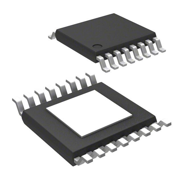
The LED6000 is available in an HTSSOP16
exposed pad package.
MLCC output capacitor
Figure 1. Application schematic
4: /$)
7*/
%*.
%*.
7*/@�
7*/@�
7#*"4
#005
7$$
-
&/
$*/
$#005
-&%����
-9@�
-9@�
7-&%�
44
$065
'#
'48
$7$$
$44
*-*.
$'
3'
(/%
36
$0.1
7-&%�
%
$1
34/4
(/%
(/%
".�����
May 2015
This is information on a product in full production.
DocID027777 Rev 2
1/49
www.st.com
�Contents
LED6000
Contents
1
Block diagram . . . . . . . . . . . . . . . . . . . . . . . . . . . . . . . . . . . . . . . . . . . . . . 4
2
Pin settings . . . . . . . . . . . . . . . . . . . . . . . . . . . . . . . . . . . . . . . . . . . . . . . . 5
2.1
Pin connection . . . . . . . . . . . . . . . . . . . . . . . . . . . . . . . . . . . . . . . . . . . . . . 5
2.2
Pin description . . . . . . . . . . . . . . . . . . . . . . . . . . . . . . . . . . . . . . . . . . . . . . 6
2.3
Maximum ratings . . . . . . . . . . . . . . . . . . . . . . . . . . . . . . . . . . . . . . . . . . . . 7
2.4
Thermal data . . . . . . . . . . . . . . . . . . . . . . . . . . . . . . . . . . . . . . . . . . . . . . . 7
2.5
ESD protection . . . . . . . . . . . . . . . . . . . . . . . . . . . . . . . . . . . . . . . . . . . . . . 7
3
Electrical characteristics . . . . . . . . . . . . . . . . . . . . . . . . . . . . . . . . . . . . . 8
4
Functional description . . . . . . . . . . . . . . . . . . . . . . . . . . . . . . . . . . . . . . 11
5
2/49
4.1
Oscillator and synchronization . . . . . . . . . . . . . . . . . . . . . . . . . . . . . . . . . .11
4.2
Soft-start . . . . . . . . . . . . . . . . . . . . . . . . . . . . . . . . . . . . . . . . . . . . . . . . . . 15
4.3
Digital dimming . . . . . . . . . . . . . . . . . . . . . . . . . . . . . . . . . . . . . . . . . . . . . 16
4.4
Error amplifier and light-load management . . . . . . . . . . . . . . . . . . . . . . . 19
4.5
Low VIN operation . . . . . . . . . . . . . . . . . . . . . . . . . . . . . . . . . . . . . . . . . . 20
4.6
Overcurrent protection . . . . . . . . . . . . . . . . . . . . . . . . . . . . . . . . . . . . . . . 21
4.7
Overtemperature protection . . . . . . . . . . . . . . . . . . . . . . . . . . . . . . . . . . . 23
Application notes - step-down conversion . . . . . . . . . . . . . . . . . . . . . . 24
5.1
Input capacitor selection . . . . . . . . . . . . . . . . . . . . . . . . . . . . . . . . . . . . . . 24
5.2
Output capacitor and inductor selection . . . . . . . . . . . . . . . . . . . . . . . . . . 25
5.3
Compensation strategy . . . . . . . . . . . . . . . . . . . . . . . . . . . . . . . . . . . . . . 27
5.4
Thermal considerations . . . . . . . . . . . . . . . . . . . . . . . . . . . . . . . . . . . . . . 30
5.5
Layout considerations . . . . . . . . . . . . . . . . . . . . . . . . . . . . . . . . . . . . . . . 31
5.6
Demonstration board . . . . . . . . . . . . . . . . . . . . . . . . . . . . . . . . . . . . . . . . 32
DocID027777 Rev 2
�LED6000
6
7
Contents
Application notes - alternative topologies . . . . . . . . . . . . . . . . . . . . . . 35
6.1
Inverting buck-boost . . . . . . . . . . . . . . . . . . . . . . . . . . . . . . . . . . . . . . . . . 35
6.2
Positive buck-boost . . . . . . . . . . . . . . . . . . . . . . . . . . . . . . . . . . . . . . . . . 38
6.3
Floating boost . . . . . . . . . . . . . . . . . . . . . . . . . . . . . . . . . . . . . . . . . . . . . . 41
6.4
Compensation strategy for alternative topologies . . . . . . . . . . . . . . . . . . 44
Package information . . . . . . . . . . . . . . . . . . . . . . . . . . . . . . . . . . . . . . . . 46
HTSSOP16 package information . . . . . . . . . . . . . . . . . . . . . . . . . . . . . . . . . . . . . 46
8
Ordering information . . . . . . . . . . . . . . . . . . . . . . . . . . . . . . . . . . . . . . . 48
9
Revision history . . . . . . . . . . . . . . . . . . . . . . . . . . . . . . . . . . . . . . . . . . . 48
DocID027777 Rev 2
3/49
49
�Block diagram
1
LED6000
Block diagram
Figure 2. Block diagram
4/49
DocID027777 Rev 2
�LED6000
Pin settings
2
Pin settings
2.1
Pin connection
Figure 3. Pin connection (top view)
DocID027777 Rev 2
5/49
49
�Pin settings
2.2
LED6000
Pin description
Table 1. Pin description
No.
1
6/49
Pin
Description
Auxiliary input that can be used to supply a part of the analog circuitry to increase the
VBIAS efficiency at the light-load. Connect to GND if not used or bypass with a 1 µF ceramic
capacitor if supplied by an auxiliary rail.
2
VIN
DC input voltage
3
VIN
DC input voltage
4
VCC
Filtered DC input voltage to the internal circuitry. Bypass to the signal GND by a 1 µF
ceramic capacitor.
5
EN
Active high enable pin. Connect to the VCC pin if not used.
6
SS
An internal current generator (5 µA typ.) charges the external capacitor to implement
the soft-start.
7
SYNCH Master / slave synchronization
8
COMP
9
FB
10
FSW
A pull-down resistor to GND selects the switching frequency.
11
ILIM
A pull-down resistor to GND selects the peak current limitation.
12
DIM
A PWM signal in this input pin implements the LED PWM current dimming. It's pulleddown by an internal 2 µA current.
13
LX
Switching node
14
LX
Switching node
15
BOOT
16
GND
Signal GND
--
E. P.
The exposed pad must be connected to the signal GND.
Output of the error amplifier. The designed compensation network is connected at
this pin.
Inverting input of the error amplifier
Connect an external capacitor (100 nF typ.) between BOOT and LX pins. The gate
charge required to drive the internal n-DMOS is recovered by an internal regulator
during the off-time.
DocID027777 Rev 2
�LED6000
2.3
Pin settings
Maximum ratings
Table 2. Absolute maximum ratings
Symbol
Min.
Max.
Unit
VIN
-0.3
61
V
VCC
-0.3
61
V
VBOOT - GND
-0.3
65
V
VBOOT - VLX
-0.3
4
V
VBIAS
-0.3
VCC
V
EN
-0.3
VCC
V
DIM
-0.3
VCC
V
LX
-0.3
VIN + 0.3
V
SYNCH
-0.3
5.5
V
SS
-0.3
3.6
V
FSW
-0.3
3.6
V
COMP
-0.3
3.6
V
ILIM
-0.3
3.6
V
FB
-0.3
3.6
V
Operating temperature range
-40
150
°C
TSTG
Storage temperature range
-65
150
°C
TLEAD
Lead temperature (soldering 10 sec.)
260
°C
3
A
BOOT
TJ
High-side RMS current
IHS
2.4
Description
Thermal data
Table 3. Thermal data
2.5
Symbol
Parameter
Value
Unit
RthJA
Thermal resistance junction ambient (device soldered on the
STMicroelectronics® demonstration board)
40
°C/W
ESD protection
Table 4. ESD protection
Symbol
Test condition
Value
Unit
ESD
HBM
2
KV
CDM
500
V
DocID027777 Rev 2
7/49
49
�Electrical characteristics
3
LED6000
Electrical characteristics
All the population tested at TJ = 25 °C, VIN = VCC = 24 V, VBIAS = GND, VDIM = VEN = 3 V
and RILIM = N. M. unless otherwise specified.
Table 5. Electrical characteristics
Symbol
VIN
Parameter
Operating input voltage
range
RDSON HS High-side RDSON
Switching frequency
fSW
IPK
ISKIP
Test condition
Min.
(1)
4.5
V
0.25
0.32
0.25
0.42
233
250
267
kHz
225
250
275
kHz
1350
1500
1650
kHz
(1)
FSW pin floating;
FSW pin floating
(1)
Max. Unit
61
ILX = 0.5 A
ILX = 0.5 A
Typ.
Selected switching
frequency
RFSW = 10 k
Peak current limit
ILIM pin floating; VFB = 0.2 V
(2)
3.5
4.1
4.7
A
Selected peak current limit
RILIM = 100 k; VFB = 0.2 V
(2)
0.68
0.85
1.01
A
ILIM pin floating
(2)
0.40
A
RILIM = 100 k
(2)
0.15
A
Pulse skipping peak current
TONMIN
Minimum on-time
TONMAX
Maximum on-time
TOFFMIN
Minimum off-time
120
Refer to Section 4: Functional
description for TONMAX details.
(3)
150
ns
12
s
360
ns
VCC / VBIAS
VCCH
(1)
3.85
4.10
4.30
V
(1)
160
250
340
mV
Switch internal supply from VCC to
VBIAS. VBIAS ramping up from 0 V.
(1)
2.82
2.90
2.98
V
Hysteresis
(3)
Switch internal supply from VCC to
VBIAS. VIN = VCC = 24 V, VBIAS falling
from 24 V to GND.
(1)
Hysteresis
(3)
VCC UVLO rising threshold
VCCHYST VCC UVLO hysteresis
VBIAS threshold
SWO
VCC -VBIAS threshold
80
3.35
4.05
mV
4.90
750
V
mV
Power consumption
ISHTDWN
Shutdown current from VIN
VEN = GND
10
15
A
IQUIESC
Quiescent current from VIN
and VCC
LX floating, VFB = 1 V,
VBIAS = GND, FSW floating.
2.4
3.4
mA
8/49
DocID027777 Rev 2
�LED6000
Electrical characteristics
Table 5. Electrical characteristics (continued)
Symbol
Parameter
IQOPVIN
Quiescent current from VIN
and VCC
IQOPVBIAS
Quiescent current from
VBIAS
Test condition
Min.
LX floating, VFB = 1 V,
VBIAS = 3.3 V, FSW floating
Typ.
Max. Unit
0.9
1.4
mA
1.5
2.4
mA
Enable
VENL
Device OFF level
0.06
0.30
V
VENH
Device ON level
0.35
0.90
V
Soft-start
TSSSETUP Soft-start setup time
ISSCH
CSS charging current
Delay from UVLO rising to switching
activity
(3)
VSS = GND
s
640
4.3
5.0
5.7
A
Error amplifier
VFB
Voltage feedback
(1)
VCOMPH
VFB = GND; VSS = 3.2 V
VCOMPL
VFB = 3.2 V; VSS = 3.2 V
IFB
FB biasing current
IOSINK
AV0
Output stage sinking
capability
Unity gain buffer configuration (FB
connected to COMP). No load on
COMP pin.
Error amplifier gain
Unity gain buffer configuration (FB
connected to COMP). No load on
COMP pin.
GBWP
0.250 0.258
V
0.240
0.250 0.260
V
3.20
3.35
3.50
V
0.1
V
50
nA
VFB = 3.6 V
VFB = GND; SS pin floating;
VCOMP = 2 V
IOSOURCE
0.242
5
(3)
3.1
mA
(3)
5
mA
(3)
100
dB
(3)
23
MHz
Synchronization (fan out: 5 slave devices max.)
fSYN MIN
Synchronization frequency
VSYNOUT Master output amplitude
VSYNOW
Output pulse width
VSYNIH
SYNCH slave high level
input threshold
VSYNIL
SYNCH slave low level
input threshold
ISYN
VSYNIW
Slave SYNCH pull-down
current
Pin FSW floating
280
ILOAD = 4 mA
2.45
kHz
ILOAD = 0 A; pin SYNCH floating
ILOAD = 0 A; pin SYNCH floating
3.8
150
215
280
V
ns
2.0
V
1.0
VSYNCH = 5 V
Input pulse width
450
150
DocID027777 Rev 2
700
950
A
ns
9/49
49
�Electrical characteristics
LED6000
Table 5. Electrical characteristics (continued)
Symbol
Parameter
Test condition
Min.
Typ.
Max. Unit
Dimming
VDIMH
DIM rising threshold
VDIML
DIM falling threshold
VDIMPD
TDIMTO
DIM pull-down current
1.23
VDIM = 2 V
Dimming timeout
0.75
1.00
0.5
1.5
1.7
V
V
2.5
A
(3)
42
ms
Thermal shutdown
TSHDWN
Thermal shutdown
temperature
(3)
170
°C
THYS
Thermal shutdown
hysteresis
(3)
15
°C
1. Specifications referred to TJ from -40 to +125 °C. Specifications in the -40 to +125 °C temperature range are assured by
design, characterization and statistical correlation.
2. Parameter tested in static condition during testing phase. Parameter value may change over dynamic application condition.
3. Not tested in production.
10/49
DocID027777 Rev 2
�LED6000
4
Functional description
Functional description
The LED6000 device is based on a voltage mode, constant frequency control loop. The
LEDs current, monitored through the voltage drop on the external current sensing resistor,
RSNS, is compared to an internal reference (0.25 V) providing an error signal on the COMP
pin. The COMP voltage level is then compared to a fixed frequency sawtooth ramp, which
finally controls the on- and off-time of the power switch.
The main internal blocks are shown in Figure 2: Block diagram on page 4 and can be
summarized as follow.
4.1
The fully integrated oscillator that provides the sawtooth ramp to modulate the duty
cycle and the synchronization signal. Its switching frequency can be adjusted by an
external resistor. The input voltage feedforward is implemented.
The soft-start circuitry to limit the inrush current during the startup phase.
The voltage mode error amplifier.
The pulse width modulator and the relative logic circuitry necessary to drive the internal
power switch.
The high-side driver for the embedded N-channel power MOSFET switch and
bootstrap circuitry. A dedicated high resistance low-side MOSFET, for anti-boot
discharge management purposes, is also present.
The peak current limit sensing block, with a programmable threshold, to handle the
overload including a thermal shutdown block, to prevent the thermal runaway.
The bias circuitry, which includes a voltage regulator and an internal reference, to
supply the internal circuitry and provide a fixed internal reference and manages the
current dimming feature. The switchover function from VCC to VBIAS can be
implemented for higher efficiency. This block also implements voltage monitor circuitry
(UVLO) that checks the input and internal voltages.
Oscillator and synchronization
Figure 4 shows the block diagram of the oscillator circuit. The internal oscillator provides
a constant frequency clock, whose frequency depends on the resistor externally connected
between the FSW pin and ground.
Figure 4. Oscillator and synchronization
DocID027777 Rev 2
11/49
49
�Functional description
LED6000
If the FSW pin is left floating, the programmed frequency is 250 kHz (typ.); if the FSW pin is
connected to an external resistor, the programmed switching frequency can be increased up
to 1.5 MHz, as shown in Figure 5. The required RFSW value (expressed in k) is estimated
by Equation 1:
Equation 1
FSW 250kHz
12500
RFSW
Figure 5. Switching frequency programmability
To improve the line transient performance, keeping the PWM gain constant versus the input
voltage, the input voltage feedforward is implemented by changing the slope of the sawtooth
ramp, according to the input voltage change (Figure 6 a).
The slope of the sawtooth also changes if the oscillator frequency is programmed by the
external resistor. In this way a frequency feedforward is implemented (Figure 6 b) in order to
keep the PWM modulator gain constant versus the switching frequency.
On the SYNCH pin the synchronization signal is generated. This signal has a phase shift of
180° with respect to the clock. This delay is useful when two devices are synchronized
connecting the SYNCH pins together. When SYNCH pins are connected, the device with
a higher oscillator frequency works as a master, so the slave device switches at the
frequency of the master but with a delay of half a period. This helps reducing the RMS
current flowing through the input capacitor. Up to five LED6000s can be connected to the
same SYNCH pin; however, the clock phase shift from master switching frequency to the
slave input clock is 180°.
The LED6000 device can be synchronized to work at a higher frequency, in the range of
250 kHz - 1500 kHz, providing an external clock signal on the SYNCH pin. The
synchronization changes the sawtooth amplitude, also affecting the PWM gain (Figure 6 c).
This change must be taken into account when the loop stability is studied. In order to
12/49
DocID027777 Rev 2
�LED6000
Functional description
minimize the change of the PWM gain, the free-running frequency should be set (with a
resistor on the FSW pin) only slightly lower than the external clock frequency.
This pre-adjusting of the slave IC switching frequency keeps the truncation of the ramp
sawtooth negligible.
In case two or more (up to five) LED6000 SYNCH pins are tied together, the LED6000 IC
with higher programmed switching frequency is typically the master device; however, the
SYNCH circuit is also able to synchronize with a slightly lower external frequency, so the
frequency pre-adjustment with the same resistor on the FSW pin, as suggested above, is
required for a proper operation.
The SYNCH signal is provided as soon as EN is asserted high; however, if DIM is kept low
for more than TDIMTO timeout, the SYNCH signal is no more available until DIM re-assertion
high.
DocID027777 Rev 2
13/49
49
�Functional description
LED6000
Figure 6. Feedforward
14/49
DocID027777 Rev 2
�LED6000
4.2
Functional description
Soft-start
The soft-start is essential to assure a correct and safe startup of the step-down converter. It
avoids an inrush current surge and makes the output voltage to increase monotonically.
The soft-start is performed as soon as the EN and DIM pin are asserted high; when this
occurs, an external capacitor, connected between the SS pin and ground, is charged by
a constant current (5 µA typ.). The SS voltage is used as reference of the switching
regulator and the output voltage of the converter tracks the ramp of the SS voltage. When
the SS pin voltage reaches the 0.25 V level, the error amplifier switches to the internal
0.25 V reference to regulate the output voltage.
Figure 7. Soft-start
During the soft-start period the current limit is set to the nominal value.
The dVSS/dt slope is programmed in agreement with Equation 2:
Equation 2
C SS
I SS TSS 5A TSS
VREF
0.25V
Before starting the CSS capacitor charge, the soft-start circuitry turns-on the discharge
switch shown in Figure 7 for TSSDISCH minimum time, in order to completely discharge the
CSS capacitor.
As a consequence, the maximum value for the soft-start capacitor, which assures an almost
complete discharge in case of the EN signal toggle, is provided by:
Equation 3
C SS _ MAX
TSSDISCH
270nF
5 RSSDISCH
given TSSDISCH = 530 µs and RSSDISCH = 380 typical values.
The enable feature allows to put the device into the standby mode. With the EN pin lower
than VENL the device is disabled and the power consumption is reduced to 10 A (typ.). If
the EN pin is higher than VENH, the device is enabled. If the EN pin is left floating, an internal
pull-down current ensures that the voltage at the pin reaches the inhibit threshold and the
device is disabled. The pin is also VCC compatible.
DocID027777 Rev 2
15/49
49
�Functional description
4.3
LED6000
Digital dimming
The switching activity is inhibited as long as the DIM pin is kept below the VDIML threshold.
When the DIM is asserted low, the HS MOS is turned-off as soon as the minimum on-time is
expired and the COMP pin is parked close to the maximum ramp peak value, in order to
limit the input inrush current when the IC restarts the switching activity. The internal
oscillator and, consequently, the IC quiescent current are reduced only if the DIM is kept low
for more than TDIMTO timeout.
The inductor current dynamic performance, when dimming input goes high, depends on the
designed system response. The best dimming performance is obtained by maximizing the
bandwidth and phase margin, when possible.
As a general rule, the output capacitor minimization improves dimming performance in
terms of the shorter LEDs current rising time and reduced inductor peak current.
An oversized output capacitor value requires an extra current for the fast charge so
generating an inductor current overshoot and oscillations.
Refer also to Section 5.2 on page 25 for output capacitor design hints.
The dimming performance depends on the current pulse shape specification of the final
application.
Figure 8. Dimming operation
The ideal current pulse has rectangular shape; however, in any case it degenerates into
a trapezoid or, at worst, into a triangle, depending on the ratio (tRISE + tFALL)/ TLED.
16/49
DocID027777 Rev 2
�LED6000
Functional description
Figure 9. Dimming operation (rising edge) - VIN = 44 V, 12 LED
Figure 10. Dimming operation (falling edge) - VIN = 44 V, 12 LED
DocID027777 Rev 2
17/49
49
�Functional description
LED6000
In Figure 11 a very short DIM pulse is shown, measured in the standard demonstration
board, VIN = 44 V, 12 LEDs. The programmed LED current, 1 A, is reached at the end of the
DIM pulse (35 µs).
Figure 11. Dimming operation - short DIM pulse
The above consideration is crucial when short DIM pulses are expected in the final
application. Once the external power components and the compensation network are
selected, a direct measurement to determine tRISE and tFALL is necessary to certify the
achieved dimming performance.
When the DIM is forced above the VDIMH threshold after TDIMTO has elapsed, a new softstart sequence is performed.
18/49
DocID027777 Rev 2
�LED6000
4.4
Functional description
Error amplifier and light-load management
The error amplifier (E/A) provides the error signal to be compared with the sawtooth to
perform the pulse width modulation. Its non-inverting input is internally connected to
a 0.25 V voltage reference and its inverting input (FB) and output (COMP) are externally
available for feedback and frequency compensation. In this device the error amplifier is
a voltage mode operational amplifier, therefore, with the high DC gain and low output
impedance.
The uncompensated error amplifier characteristics are summarized inTable 6.
Table 6. Error amplifier characteristics
Parameters
Value
Low frequency gain (A0)
100 dB
GBWP
23 MHz
Output voltage swing
0 to 3.5 V
Source/sink current capability
3.1 mA / 5 mA
In the continuous conduction working mode (CCM), the transfer function of the power
section has two poles due to the LC filter and one zero due to the ESR of the output
capacitor. Different kinds of compensation networks can be used depending on the ESR
value of the output capacitor.
If the zero introduced by the output capacitor helps to compensate the double pole of the LC
filter, a type II compensation network can be used. Otherwise, a type III compensation
network must be used (see Section 5.3 on page 27 for details on the compensation network
design).
In case of the light-load (i.e.: if the output current is lower than the half of the inductor current
ripple) the LED6000 enters the pulse-skipping working mode. The HS MOS is kept off if the
COMP level is below 200 mV (typ.); when this bottom level is reached the integrated switch
is turned on until the inductor current reaches ISKIP value. So, in the discontinuous
conduction working mode (DCM), the HS MOS on-time is only related to the time necessary
to charge the inductor up to the ISKIP level.
The ISKIP threshold is reduced with increasing the RILIM resistor value, as shown also in
Table 5 on page 8 and plotted in Figure 12, so allowing the LED6000 device work in the
continuous conduction mode also in case lower current LEDs are selected.
DocID027777 Rev 2
19/49
49
�Functional description
LED6000
Figure 12. ISKIP typical current and RILIM value
However, due to the current sensing comparator delay, the actual inductor charge current is
slightly impacted by the VIN and selected inductor value.
In order to let the bootstrap capacitor recharge, in case of an extremely light-load the
LED6000 is able to pull-down the LX net through an integrated small LS MOS. In this way
the bootstrap recharge current can flow from the VIN through the CBOOT, LX and LS MOS.
This mechanism is activated if the HS MOS has been kept turned-off for more than 3 ms
(typ.).
4.5
Low VIN operation
In normal operation (i.e.: VOUT programmed lower than input voltage) when the HS MOS is
turned off, a minimum off time (TOFFMIN) interval is performed.
In case the input voltage falls close or below the programmed output voltage (low dropout,
LDO) the LED6000 control loop is able to increase the duty cycle up to 100%. However, in
order to keep the boot capacitor properly recharged, a maximum HS MOS on-time is limited
(TONMAX). When this limit is reached the HS MOS is turned-off and an integrated switch
working as a pull-down resistor between the LX and GND is turned on, until one of the
following conditions is met:
A negative current limit (300 mA typ.) is reached
A timeout (1 µs typ.) is reached.
So doing the LED6000 device is able to work in the low dropout operation, due to the
advanced boot capacitor management, and the effective maximum duty cycle is about
12 s / 13 s = 92%.
20/49
DocID027777 Rev 2
�LED6000
4.6
Functional description
Overcurrent protection
The LED6000 implements overcurrent protection by sensing the current flowing through the
power MOSFET. Due to the noise created by the switching activity of the power MOSFET,
the current sensing circuitry is disabled during the initial phase of the conduction time. This
avoids erroneous detection of fault condition. This interval is generally known as “masking
time” or “blanking time”. The masking time is about 120 ns.
If the overcurrent limit is reached, the power MOSFET is turned off implementing pulse by
pulse overcurrent protection. In the overcurrent condition, the device can skip turn-on pulses
in order to keep the output current constant and equal to the current limit. If, at the end of the
“masking time”, the current is higher than the overcurrent threshold, the power MOSFET is
turned off and one pulse is skipped. If, at the following switching on, when the “masking
time” ends, the current is still higher than the overcurrent threshold, the device skips two
pulses. This mechanism is repeated and the device can skip up to seven pulses (refer to
Figure 13).
If at the end of the “masking time” the current is lower than the overcurrent threshold, the
number of skipped cycles is decreased by one unit.
As a consequence, the overcurrent protection acts by turning off the power MOSFET and
reducing the switching frequency down to one eighth of the default switching frequency, in
order to keep constant the output current close to the current limit.
Figure 13. OCP and frequency scaling
This kind of overcurrent protection is effective if the inductor can be completely discharged
during HS MOS turn-off time, in order to avoid the inductor current to run away. In case of
the output short-circuit the maximum switching frequency can be computed by the following
equation:
Equation 4
FSW ,MAX
8 VF RDCR I LIM
1
VIN RON RDCR I LIM TON ,MIN
DocID027777 Rev 2
21/49
49
�Functional description
LED6000
Assuming VF = 0.6 V the free-wheeling diode direct voltage, RDCR = 30 m inductor
parasitic resistance, ILIM = IPK = 4 A the peak current limit, RON = 0.25 HS MOS
resistance and TON,MIN = 120 ns minimum HS MOS on duration, the maximum FSW
frequency which avoids the inductor current runaway in case of the output short-circuit and
VIN = 61 V is 801 kHz.
If the programmed switching frequency is higher than the above computed limit, an
estimation of the inductor current in case of the output short-circuit fault is provided by
Equation 5:
Equation 5
I LIM
FSW TON VIN 8 VF
8 RDCR FSW TON ,MIN RON RDCR
The peak current limit threshold (ILIM) can be programmed in the range 0.85 A - 4.0 A by
selecting the proper RILIM resistor, as suggested in Equation 6.
Equation 6
RILIM 20k
I PK
I LIM
IPK is the default LED6000 current limit in case of RILIM not mounted, as shown in Table 5 on
page 8.
Figure 14. Current limit and programming resistor
22/49
DocID027777 Rev 2
�LED6000
4.7
Functional description
Overtemperature protection
It is recommended that the device never exceeds the maximum allowable junction
temperature. This temperature increase is mainly caused by the total power dissipated by
the integrated power MOSFET.
To avoid any damage to the device when reaching high temperature, the LED6000
implements a thermal shutdown feature: when the junction temperature reaches 170 °C
(typ.) the device turns off the power MOSFET and shuts-down.
When the junction temperature drops to 155 °C (typ.), the device restarts with a new softstart sequence.
DocID027777 Rev 2
23/49
49
�Application notes - step-down conversion
LED6000
5
Application notes - step-down conversion
5.1
Input capacitor selection
The input capacitor must be rated for the maximum input operating voltage and the
maximum RMS input current.
Since the step-down converters input current is a sequence of pulses from 0A to IOUT, the
input capacitor must absorb the equivalent RMS current which can be up to the load current
divided by two (worst case, with duty cycle of 50%). For this reason, the quality of these
capacitors must be very high to minimize the power dissipation generated by the internal
ESR, thereby improving system reliability and efficiency.
The RMS input current (flowing through the input capacitor) in step-down conversion is
roughly estimated by:
Equation 7
I CIN , RMS I OUT D 1 D
The actual DC/DC conversion duty cycle, D = VOUT/VIN, is influenced by a few parameters:
Equation 8
DMAX
VOUT VF
VIN ,MIN VSW ,MAX
DMIN
VOUT VF
VIN ,MAX VSW ,MIN
where VF is the freewheeling diode forward voltage and VSW the voltage drop across the
internal high-side MOSFET. Considering the range DMIN to DMAX it is possible to determine
the maximum ICIN,RMS flowing through the input capacitor.
The input capacitor value must be dimensioned to safely handle the input RMS current and
to limit the VIN and VCC ramp-up slew rate to 0.5 V/µs maximum, in order to avoid the
device active ESD protections turn-on.
24/49
DocID027777 Rev 2
�LED6000
Application notes - step-down conversion
Different capacitors can be considered:
Electrolytic capacitors
These are the most commonly used due to their low cost and wide range of operative
voltage. The only drawback is that, considering ripple current rating requirements, they are
physically larger than other capacitors.
Ceramic capacitors
If available for the required value and voltage rating, these capacitors usually have a higher
RMS current rating for a given physical dimension (due to the very low ESR). The drawback
is their high cost.
Tantalum capacitor
Small, good quality tantalum capacitors with very low ESR are becoming more available.
However, they can occasionally burn if subjected to a very high current, for example when
they are connected to the power supply.
The amount of the input voltage ripple can be roughly overestimated by Equation 9.
Equation 9
VIN , PP
D 1 D I OUT
RES , IN I OUT
C IN FSW
In case of MLCC ceramic input capacitors, the equivalent series resistance (RES,IN) is
negligible.
In addition to the above considerations, a ceramic capacitor with an appropriate voltage
rating and with a value 1 µF or higher should always be placed across VIN and power
ground and across VCC and the IC GND pins, as close as possible to the LED6000 device.
This solution is necessary for spike filtering purposes.
5.2
Output capacitor and inductor selection
The output capacitor is very important in order to satisfy the output voltage ripple
requirement. Using a small inductor value is useful to reduce the size of the choke but
increases the current ripple. So, to reduce the output voltage ripple, a low ESR capacitor is
required.
The current in the output capacitor has a triangular waveform which generates a voltage
ripple across it. This ripple is due to the capacitive component (charge and discharge of the
output capacitor) and the resistive component (due to the voltage drop across its ESR). So
the output capacitor must be selected in order to have a voltage ripple compliant with the
application requirements.
The allowed LED current ripple (ILED,PP) is typically from 2% to 5% of the LED DC current.
DocID027777 Rev 2
25/49
49
�Application notes - step-down conversion
LED6000
Figure 15. LEDs small signal model
Based on the small signal model typically adopted for LEDs (as shown in Figure 15), the
amount of the inductor current ripple which flows through the LEDs can be estimated by the
following equation:
Equation 10
I LED s I L s
1 sCO RES
1 sCO RES RSNS N Rd
The typical LED dynamic resistance, for high current LEDs, is about 0.9 to 1 .
The output capacitor, CO, is typically an MLCC ceramic capacitor in the range of 1 µF and
with equivalent series resistance lower than 10 m, as a consequence the zero due to the
time constant CO * RES is in the range of 10 MHz or above.
Starting from Equation 10 it's possible to roughly estimate the required CO value:
Equation 11
CO
8
2
I L ,PP
2 f SW RSNS
1
N Rd I LED,PP
In the above equation it has been assumed that the total inductor current ripple is well
approximated by the first Fourier harmonic, 8/2 * IL,PP, due to the inductor current
triangular shape.
The inductance value fixes the current ripple flowing through the output capacitor and LEDs.
So the minimum inductance value, in order to have the expected current ripple, must be
selected.
The rule to fix the current ripple value is to have a ripple at 30% - 60% of the programmed
LEDs current.
In the continuous conduction mode (CCM), the required inductance value can be calculated
by Equation 12.
26/49
DocID027777 Rev 2
�LED6000
Application notes - step-down conversion
Equation 12
V
VOUT 1 OUT
VIN
L
I L FSW
In order to guarantee a maximum current ripple in every condition, Equation 12 must be
evaluated in case of maximum input voltage, assuming VOUT fixed.
Increasing the value of the inductance helps to reduce the current ripple but, at the same
time, strongly impacts the converter response time in case of high frequency dimming
requirements. On the other hand, with a lower inductance value the regulator response time
is improved but the power conversion efficiency is impacted and the output capacitor must
be increased to limit the current ripple flowing through the LEDs.
As usually, the L-CO choice is a trade-off among multiple design parameters.
5.3
Compensation strategy
The compensation network must assure stability and good dynamic performance. The loop
of the LED6000 is based on the voltage mode control. The error amplifier is an operational
amplifier with high bandwidth. So, by selecting the compensation network the E/A is
considered as ideal, that is, its bandwidth is much larger than the system one.
Figure 16. Switching regulator control loop simplified model
DocID027777 Rev 2
27/49
49
�Application notes - step-down conversion
LED6000
The transfer function of the PWM modulator, from the error amplifier output (COMP pin) to
the LX pin results in an almost constant gain, due to the voltage feedforward which
generates a sawtooth with amplitude VS directly proportional to the input voltage:
Equation 13
G PW 0
1
1
VS k FF VIN
For the LED6000 the feedforward gain is KFF = 1/30.
The synchronization of the device with an external clock provided through the SYNCH pin
can modify the PWM modulator gain (see Section 4.1 on page 11 to understand how this
gain changes and how to keep it constant in spite of the external synchronization).
The transfer function of the power section (i.e.: the voltage across RSNS resulting as
a variation of the duty cycle) is:
Equation 14
G LC ( s )
VSNS ( s )
d ( s)
RSNS V IN
RSNS s L R DC N Rd //
1 s C O R ES
s CO
given L, RDC, CO, RES, RSNS and Rd the parameters shown in Figure 16.
The power section transfer function can be rewritten as follows:
Equation 15
1
G LC ( s ) G LC 0
1
s
2 f z
s
s
2 Q f LC 2 f LC
2
; G LC 0
RSNS V IN
RSNS N Rd
Equation 16
fz
1
;
2 CO RES N Rd
1
f LC
2 LCO
N Rd
N Rd RSNS
Equation 17
Q
LCO RSNS N Rd N Rd
L CO RSNS N Rd
with the assumption that the inductor parasitic resistance, RDC, and the output capacitor
parasitic resistance, RES, are negligible compared to LED dynamic resistance, Rd.
The closed loop gain is then given by:
Equation 18
GLOOP (s) GLC (s) GPW 0 (s) GCOMP (s)
28/49
DocID027777 Rev 2
�LED6000
Application notes - step-down conversion
As shown in Equation 16, fz depends on the output capacitor parasitic resistance and on the
LEDs dynamic resistance. Following the considerations summarized in Section 5.2 on
page 25, in the typical application the programmed control loop bandwidth (BW) might be
higher than fz, so this zero helps stabilize the loop. If this assumption is verified, a type II
compensation network is required for loop stabilization.
In Figure 17 the type II compensation network is shown.
Figure 17. Type II compensation network
The type II compensation network transfer function, from VSNS to COMP, is computed in
Equation 19.
Equation 19
Equation 20
f Z1
1
;
2 C F RF
f P0
1
;
2 C F C P RU
f P1
1
2 C F // C P RF
The following suggestions can be followed for a quite common compensation strategy,
assuming that CP


 工商网监
湘ICP备2023018690号
工商网监
湘ICP备2023018690号
