LED8102S
Datasheet
8-channel LED driver with direct switch control
Features
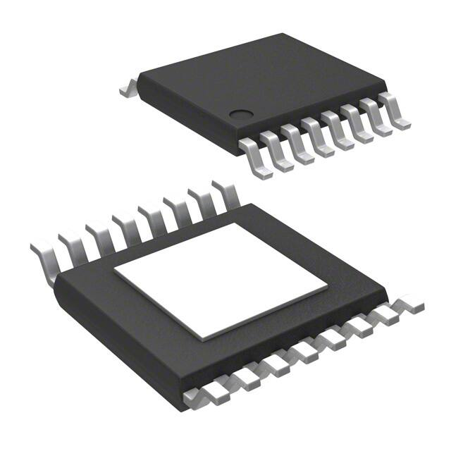
HTSSOP16
(Exposed pad)
•
•
•
•
•
•
•
•
•
8 constant current output channels controlled by switch inputs
Output enable input for global dimming
Output current: from 5 mA to 100 mA
Current programmable through external resistor
Supply voltage: 3 V to 5.5 V
Thermal shutdown
19 V current generators rated voltage
Available in high thermal efficiency TSSOP exposed pad package
ESD protection 2.0 kV HBM, 100 V MM
Applications
•
White and RGB lighting and Backlight
–
Appliance display and human interface
–
Industrial display and function indicator
–
Architectural Lighting
Description
Maturity status link
LED8102S
Device summary
Order code
LED8102SXTTR
Package
HTSSOP16
Packing
2500 parts per reel
The LED8102S is a monolithic, low voltage, 8 low-side-channel LED driver. The
LED8102S guarantees up to 19 V output driving capability allowing users to connect
several LEDs in series. In the output stage, 8 regulated current sources provide from
5 mA to 100 mA constant current to drive the LEDs. Current is programmed through
a single external resistor.
LED8102S is equipped with a thermal management that protects the device forcing
it in shutdown (typically: power-off at 170 °C with 15 °C hysteresis to restart). The
thermal protection switches OFF only the output channels.
The operative supply voltage range is between 3 V and 5.5 V. The output control
is provided by four switch inputs, providing an on/off toggle action suitable also for
local dimming. Moreover, on all active output LEDs brightness can be adjusted with a
global PWM signal applied to the output enable pin (OE). Outputs can be connected
in parallel, or left unconnected if not used, as required by the application.
DS12963 - Rev 3 - February 2021
For further information contact your local STMicroelectronics sales office.
www.st.com
�LED8102S
Pin description
1
Pin description
Figure 1. Pinout for HTSSOP16
GND
VDD
SW1
R-EXT
SW2
OE
SW3
SW4
OUT0
OUT7
OUT1
OUT6
OUT2
OUT5
OUT3
OUT4
Table 1. Pin description
DS12963 - Rev 3
HTSSOP16
Symbol
1
GND
Ground terminal
2
SW1
Switch input 1 to enable OUT0 and OUT1 simultaneously
3
SW2
Switch input 2 to enable OUT2 and OUT3 simultaneously
4
SW3
Switch input 3 to enable OUT4 and OUT5 simultaneously
5-12
OUT0-OUT7
13
SW4
14
OE
15
R-EXT
16
VDD
Name and function
Output terminals
Switch input 4 to enable OUT6 and OUT7 simultaneously
Global PWM brightness control input terminal (it must be connected to GND if
not used)
Terminal for external resistor for constant current programming
Supply voltage terminal
page 2/20
�LED8102S
Simplified internal block diagram
2
Simplified internal block diagram
Figure 2. LED8102S simplified block diagram
SWx
DS12963 - Rev 3
page 3/20
�LED8102S
Absolute maximum ratings
3
Absolute maximum ratings
Stressing the device above the ratings listed in the table below may cause permanent damage to the device.
These are stress ratings only and operation of the device at these or any other conditions above those indicated
in the Operating sections of this specification is not implied. Exposure to Absolute Maximum Rating conditions for
extended periods may affect device reliability.
Table 2. Absolute maximum ratings
Symbol
VDD
Parameter
Value
Unit
0 to 7
V
- 0.4 to 5.5
V
- 0.5 to 20
V
GND terminal current
800
mA
Electrostatic discharge protection HBM human body model
±2
kV
Electrostatic discharge protection CDM machine model
500
V
Value
Unit
Supply voltage
VSW1- VSW4, VOE Input pins voltage
VOUT0 - OUT7
IGND
ESD
3.1
Output pins voltage
Thermal characteristics
Table 3. Thermal characteristics
Symbol
TJ
TSTG
Rthj-amb
Parameter
Operative junction temperature range
-40 to +150
Storage ambient temperature range
-55 to +150
Thermal resistance junction-ambient (HTSSOP16) (1)
37.5
°C
°C/W
1. The exposed pad should be soldered directly to the PCB to realize the thermal benefits
DS12963 - Rev 3
page 4/20
�LED8102S
Electrical characteristics
4
Electrical characteristics
VDD = 5 V, Tj = 25 °C, REXT = 980 Ω, VO = 0.85 V unless otherwise specified.
Table 4. Electrical characteristics
Symbol
Parameter
VDD
Supply voltage
Conditions
Min.
Typ.
Max.
3.0
-
5.5
2.7
2.9
UVLO threshold (rising)
VUVLO
UVLO threshold (falling)
HyUVLO
2.1
UVLO hysteresis
VO
Output voltage
VIH
2.3
0.4
(1) (2)
OUT0 – OUT7
SWx / OE input voltage
VIL
V
0.85
-
19
0.8VDD
-
VDD
GND
-
0.2VDD
RUP
Pull-up resistor for OE pin
-
300
-
RDW
Pull-down resistor for SWx pins
-
310
-
REXT
External current set-up resistance
0.19
-
3.9
-
7
8
-
14
16
IDD(OFF1)
OUT0 to 7 = OFF
Supply current (OFF)
IDD(OFF2)
REXT = 190 Ω
OUT0 to 7 = OFF
Supply current (ON)
-
14
16
VO from 1 V to 3 V;
-
0.1
-
VO = 1.4 V
KΩ
mA
REXT = 190 Ω
IDD(ON)
Unit
OUT0 to 7 = ON
%/dVO
Output current vs. outputvoltage regulation
%/dVDD
Output current vs. supply voltage regulation (1) (4)
VDD from 3 V to 5.5 V
-
1
-
∆IOL
Output current precision: device to device (1)
VO = 0.3 V; REXT = 3.9 kΩ
-
-
±6
VO = 0.7 V
-
±1.5
±4
VO = 1.4 V; REXT = 190 Ω
-
±1.2
±4
VO = 19 V OUTn = OFF
-
0.5
2
∆IOL1
∆IOL2
(1) (3)
Output current precision: channel to channel (1) (5)
|%/V|
%
%
IOleak
Single output leakage current
Tsd
Thermal shutdown (6)
170
°C
Tsd_hys
Thermal shutdown hysteresis (6)
15
°C
µA
1. Test with just one output ON.
2. Minimum regulation voltage @ IO = 50 mA.
3.
4.
Δ % /V =
Δ % /V
=
Ion@Von3.0V − Ion@Von1.0V
× 3100
−1
Ion@Von = 1.0V
Ion@VDD = 5.5V − Ion@VDD = 3.0V
× 100
5.5 − 3.0
Ion@VDD = 3.0V
5. ((IOn – IOavg0-7)/ IOavg0-7) x 100.
6. Not tested in production.
DS12963 - Rev 3
page 5/20
�LED8102S
Switching characteristics
5
Switching characteristics
VDD = 5 V, Tj = 25 °C, IO = 50 mA, RL = 60 Ω, CL = 10 pF, VL = 5 V, unless otherwise specified.
Table 5. Switching characteristics
Symbol
tPLH1
tPLH2
tPHL1
tPHL2
tON
tOFF
Parameter
Conditions
Min.
Typ.
Max.
SWx – OUTn
Propagation delay time
VDD = 3.3 V
-
220
500
(OE just “0”)
(“L” to “H”)
VDD = 5 V
-
200
500
OE - OUTn
Propagation delay time
VDD = 3.3 V
-
90
250
(SWx just “1”)
(“L” to “H”)
VDD = 5 V
-
100
250
SWx – OUTn
Propagation delay time
VDD = 3.3 V
-
100
250
(OE just “0”)
(“H” to “L”)
VDD = 5 V
-
100
250
OE - OUTn
Propagation delay time
VDD = 3.3 V
-
220
500
(SWx just “1”)
(“H” to “L”)
VDD = 5 V
-
220
500
OUTn Current rise time.
VDD = 3.3 V
-
430
600
Evaluated as OUTn falling time
VDD = 5 V
-
400
600
OUTn current fall time.
VDD = 3.3 V
-
430
600
Evaluated as OUTn rising time
VDD = 5 V
-
400
600
Unit
ns
Figure 3. tON - tOFF time evaluation
90%
OUTn
90%
10%
tON
IOUTn
DS12963 - Rev 3
10%
tOFF
ON
OFF
page 6/20
�LED8102S
Switching characteristics
Figure 4. tPLH - tPHL time evaluation
50%
50%
SWn
tPHL1
tPLH1
90%
OUTn
10%
tPHL2
OE
DS12963 - Rev 3
tPLH2
50%
50%
page 7/20
�LED8102S
Internal block diagram
6
Internal block diagram
Inputs OE and SWx terminals have pull-up and pull-down connection respectively:
Figure 5. OE Terminal
VDD
300 KW
OE
1 KW
GND
Figure 6. SWx Terminals
VDD
1 KW
SWx
300 KW
GND
DS12963 - Rev 3
page 8/20
�LED8102S
The switch output control
7
The switch output control
All switch inputs (SWx) are pulled down by a 300 kΩ. If the generic SWx pin is left floating or connected to GND
or polarized at low logic level, the corresponding outputs will be in OFF condition. If SWx pin is connected to VDD
or polarized at high logic level, the corresponding outputs will be in ON condition. See below the complete truth
table:
Table 6. Switches output control
Switch inputs
Outputs controlled (ON/OFF)
SW1
OUT0 and OUT1 simultaneously
SW2
OUT2 and OUT3 simultaneously
SW3
OUT4 and OUT5 simultaneously
SW4
OUT6 and OUT7 simultaneously
Table 7. Switches versus output truth table
DS12963 - Rev 3
SW4
SW3
SW2
SW1
OE
Out0
Out1
Out2
Out3
Out4
Out5
Out6
Out7
0
0
0
0
x
off
off
off
off
off
off
off
off
0
0
0
1
0
on
on
off
off
off
off
off
off
0
0
1
0
0
off
off
on
on
off
off
off
off
0
0
1
1
0
on
on
on
on
off
off
off
off
0
1
0
0
0
off
off
off
off
on
on
off
off
0
1
0
1
0
on
on
off
off
on
on
off
off
0
1
1
0
0
off
off
on
on
on
on
off
off
0
1
1
1
0
on
on
on
on
on
on
off
off
1
0
0
0
0
off
off
off
off
off
off
on
on
1
0
0
1
0
on
on
off
off
off
off
on
on
1
0
1
0
0
off
off
on
on
off
off
on
on
1
0
1
1
0
on
on
on
on
off
off
on
on
1
1
0
0
0
off
off
off
off
on
on
on
on
1
1
0
1
0
on
on
off
off
on
on
on
on
1
1
1
0
0
off
off
on
on
on
on
on
on
1
1
1
1
0
on
on
on
on
on
on
on
on
x
x
x
x
1
off
off
off
off
off
off
off
off
page 9/20
�LED8102S
LED current settings
8
LED current settings
The current drawn each OUTn channel is set by RSET resistor value according to the following formula:
IOUT = 1.2/Rext * 16
Driver headroom voltage
In order to correctly regulate the channel current, a minimum output voltage (VHEADROOM) across each current
generator must be guaranteed.
Figure 7, shows the minimum VHEADROOM slightly less than the target value (output MOS transistor in triode
region).
If the VHEADROOM is lower than the minimum recommended, the regulation of a current is lower than the expected
one. However an excess of VHEADROOM increases the power dissipation.
Figure 7. Minimum Vheadroom vs. IOUT (TJ = 25 °C)
120
Iout [mA]
100
80
60
40
20
0
0
200
400
600
800
1000
1200
Vheadroom min. [mV]
DS12963 - Rev 3
page 10/20
�LED8102S
Typical application
9
Typical application
Figure 8. Typical application circuit
Typical application circuit
The figure above shows a typical application schematic for ALED8102S, Cled value depends on common rail
voltage connection length and driver total output current, typically it is around 47 µF; Cin is about 1 µF; current
setting resistor depends on outputs current set (ex. with REXT = 386 Ω → IO ≈ 50 mA). The external programming
resistor between R-EXT and GND should be connected as close as possible to the device.
To have proper device functionality it is strongly suggested to follow a correct power-up sequence: VDD and VLED
power supplies must be provided simultaneously or at least, VDD must be connected before VLED to activate all
internal digital control blocks earlier than LEDs power supply. If VLED anticipates driver VDD, this could result in a
visible flash on connected LEDs (output stage undesired activation).
Device thermal management
The aim of this section is just to provide some recommendation that can be useful in designing the application
PCB for a better power dissipation:
•
To decrease the device working temperature it is necessary solder the package exposed pad to the board.
•
For better thermal performances at least a 4 layers (e.g. 2S2P) PCB should be used.
•
The copper area below the package thermal pad should be enlarged as much as possible also outside the
package perimeter (using the package sides without pins)
•
A reasonable number of vias must connect the copper area below the package to all available PCB layers
especially just below the device package (e.g. 3x3 or 4x3 vias array) but also outside package perimeter.
Smaller and closely spaced vias is a good solution. Best implementation is represented by copper filled vias.
•
On each inner layers a copper area must be provided for dissipation (wider it's better, if possible at least
4 times or more the package dimensions). A good condition is to have at least a power layer as an entire
copper area (e.g. GND layer)
•
Traces for pins connection must be enlarged as much as layout constrains allow
•
Several devices in power dissipation on the same board must be adequately spaced.
Figure 3 shows, once the maximum power dissipation is fixed, which ambient temperature range can be covered
according to maximum junction temperature and package thermal resistance: 37.5 °C/W for HTSSOP16 on Jedec
PCB (2S2P) and conditions. With same thermal resistance, figure 4 shows the junction temperature as a function
of ambient temperature considering 1 W of power dissipation.
DS12963 - Rev 3
page 11/20
�LED8102S
Typical application
Figure 9. Power dissipation rating vs ambient temperature (Rth = 37.5 °C/W; Tj = 125 °C)
5.00
4.50
4.00
Tj=125 °C
Rth=37.5 °C/W
Pd [ W ]
3.50
3.00
2.50
2.00
1.50
1.00
0.50
0.00
-40
-20
0
20
40
60
80
100
120
140
Ta [ °C ]
Figure 10. Junction temperature vs ambient temperature (Rth = 37.5°C/W; Pd = 1 W)
140
120
Tj [ °C/W ]
100
80
Pd=1W
Rth=37.5 °C/W
60
40
20
0
-40
-20
0
20
40
60
80
100
120
140
Ta [ °C ]
DS12963 - Rev 3
page 12/20
�LED8102S
Package information
10
Package information
In order to meet environmental requirements, ST offers these devices in different grades of ECOPACK packages,
depending on their level of environmental compliance. ECOPACK specifications, grade definitions and product
status are available at: www.st.com. ECOPACK is an ST trademark.
DS12963 - Rev 3
page 13/20
�LED8102S
HTSSOP16 package information
10.1
HTSSOP16 package information
Figure 11. HTSSOP16 exposed pad package outline
7419276_B
Table 8. HTSSOP16 exposed pad mechanical data
Dim.
mm.
Min.
Max
A
1.20
A1
0.15
A2
0.80
b
0.19
0.30
c
0.09
0.20
D
4.90
5.00
5.10
D1
2.80
3.00
3.20
E
6.20
6.40
6.60
E1
4.30
4.40
4.50
E2
2.80
3.00
3.20
e
L
k
aaa
1.00
1.05
0.65
0.45
L1
DS12963 - Rev 3
Typ.
0.60
0.75
1.00
0.00
8.00
0.10
page 14/20
�LED8102S
HTSSOP16 packing information
10.2
HTSSOP16 packing information
Figure 12. HTSSOP16 tape and reel outline
Table 9. HTSSOP16 tape and reel mechanical data
Dim.
mm.
Min.
A
Max.
330
C
12.8
D
20.2
N
60
T
DS12963 - Rev 3
Typ.
13.2
22.4
Ao
6.7
6.9
Bo
5.3
5.5
Ko
1.6
1.8
Po
3.9
4.1
P
7.9
8.1
page 15/20
�LED8102S
Revision history
Table 10. Document revision history
Date
Revision
29-Apr-2019
1
06-Apr-2020
2
Changes
First release.
Minor text changed in description on the cover page.
Updated footnote (4).
Updated:
26-Feb-2021
3
- Features and description on the cover page.
- Figure 1 and Figure 7.
- Table 2, Table 3, Switching characteristics and Section 8 .
DS12963 - Rev 3
page 16/20
�LED8102S
Contents
Contents
1
Pin description . . . . . . . . . . . . . . . . . . . . . . . . . . . . . . . . . . . . . . . . . . . . . . . . . . . . . . . . . . . . . . . . . . . .2
2
Simplified internal block diagram . . . . . . . . . . . . . . . . . . . . . . . . . . . . . . . . . . . . . . . . . . . . . . . . . . 3
3
Absolute maximum ratings . . . . . . . . . . . . . . . . . . . . . . . . . . . . . . . . . . . . . . . . . . . . . . . . . . . . . . . . 4
3.1
Thermal characteristics . . . . . . . . . . . . . . . . . . . . . . . . . . . . . . . . . . . . . . . . . . . . . . . . . . . . . . . . . 4
4
Electrical characteristics. . . . . . . . . . . . . . . . . . . . . . . . . . . . . . . . . . . . . . . . . . . . . . . . . . . . . . . . . . . 5
5
Switching characteristics . . . . . . . . . . . . . . . . . . . . . . . . . . . . . . . . . . . . . . . . . . . . . . . . . . . . . . . . . . 6
6
Internal block diagram . . . . . . . . . . . . . . . . . . . . . . . . . . . . . . . . . . . . . . . . . . . . . . . . . . . . . . . . . . . . . 8
7
Register description . . . . . . . . . . . . . . . . . . . . . . . . . . . . . . . . . . . . . . . . . . . . . . . . . . . . . . . . . . . . . . . 9
8
LED current settings. . . . . . . . . . . . . . . . . . . . . . . . . . . . . . . . . . . . . . . . . . . . . . . . . . . . . . . . . . . . . .10
9
Typical application. . . . . . . . . . . . . . . . . . . . . . . . . . . . . . . . . . . . . . . . . . . . . . . . . . . . . . . . . . . . . . . .11
10
Package information. . . . . . . . . . . . . . . . . . . . . . . . . . . . . . . . . . . . . . . . . . . . . . . . . . . . . . . . . . . . . .13
10.1
HTSSOP16 package information . . . . . . . . . . . . . . . . . . . . . . . . . . . . . . . . . . . . . . . . . . . . . . . . 14
10.2
HTSSOP16 packing information . . . . . . . . . . . . . . . . . . . . . . . . . . . . . . . . . . . . . . . . . . . . . . . . . 15
Revision history . . . . . . . . . . . . . . . . . . . . . . . . . . . . . . . . . . . . . . . . . . . . . . . . . . . . . . . . . . . . . . . . . . . . . . .16
DS12963 - Rev 3
page 17/20
�LED8102S
List of tables
List of tables
Table 1.
Table 2.
Table 3.
Table 4.
Table 5.
Table 6.
Table 7.
Table 8.
Table 9.
Table 10.
Pin description. . . . . . . . . . . . . . . . . . . .
Absolute maximum ratings . . . . . . . . . . .
Thermal characteristics. . . . . . . . . . . . . .
Electrical characteristics . . . . . . . . . . . . .
Switching characteristics. . . . . . . . . . . . .
Switches output control. . . . . . . . . . . . . .
Switches versus output truth table . . . . . .
HTSSOP16 exposed pad mechanical data
HTSSOP16 tape and reel mechanical data
Document revision history . . . . . . . . . . . .
DS12963 - Rev 3
.
.
.
.
.
.
.
.
.
.
.
.
.
.
.
.
.
.
.
.
.
.
.
.
.
.
.
.
.
.
.
.
.
.
.
.
.
.
.
.
.
.
.
.
.
.
.
.
.
.
.
.
.
.
.
.
.
.
.
.
.
.
.
.
.
.
.
.
.
.
.
.
.
.
.
.
.
.
.
.
.
.
.
.
.
.
.
.
.
.
.
.
.
.
.
.
.
.
.
.
.
.
.
.
.
.
.
.
.
.
.
.
.
.
.
.
.
.
.
.
.
.
.
.
.
.
.
.
.
.
.
.
.
.
.
.
.
.
.
.
.
.
.
.
.
.
.
.
.
.
.
.
.
.
.
.
.
.
.
.
.
.
.
.
.
.
.
.
.
.
.
.
.
.
.
.
.
.
.
.
.
.
.
.
.
.
.
.
.
.
.
.
.
.
.
.
.
.
.
.
.
.
.
.
.
.
.
.
.
.
.
.
.
.
.
.
.
.
.
.
.
.
.
.
.
.
.
.
.
.
.
.
.
.
.
.
.
.
.
.
.
.
.
.
.
.
.
.
.
.
.
.
.
.
.
.
.
.
.
.
.
.
.
.
.
.
.
.
.
.
.
.
.
.
.
.
.
.
.
.
.
.
.
.
.
.
.
.
.
.
.
.
.
.
.
.
.
.
.
.
.
.
.
.
.
.
.
.
.
.
.
.
.
.
.
.
.
.
.
.
.
.
.
.
.
.
.
.
.
.
.
.
.
.
.
.
.
.
.
.
.
.
.
.
.
.
.
.
.
.
.
.
.
.
.
.
.
.
.
.
.
.
.
.
.
.
.
.
.
.
.
.
.
.
.
.
.
.
.
.
.
.
.
.
.
.
.
.
.
.
.
.
.
.
.
.
.
.
.
.
.
.
.
.
.
.
.
.
.
.
.
.
.
.
.
.
.
.
.
.
.
.
.
.
.
.
.
.
.
.
.
.
.
.
.
.
.
.
.
.
.
.
.
.
.
.
.
.
.
.
.
.
.
.
.
.
.
.
.
.
.
.
.
.
.
.
.
.
.
.
.
.
.
.
.
.
.
.
.
.
.
.
.
.
.
.
.
.
.
.
. 2
. 4
. 4
. 5
. 6
. 9
. 9
14
15
16
page 18/20
�LED8102S
List of figures
List of figures
Figure 1.
Figure 2.
Figure 3.
Figure 4.
Figure 5.
Figure 6.
Figure 7.
Figure 8.
Figure 9.
Figure 10.
Figure 11.
Figure 12.
DS12963 - Rev 3
Pinout for HTSSOP16 . . . . . . . . . . . . . . . . . . . . . . . . . . . . . . . . . . . . . . . . .
LED8102S simplified block diagram . . . . . . . . . . . . . . . . . . . . . . . . . . . . . . .
tON - tOFF time evaluation. . . . . . . . . . . . . . . . . . . . . . . . . . . . . . . . . . . . . . .
tPLH - tPHL time evaluation . . . . . . . . . . . . . . . . . . . . . . . . . . . . . . . . . . . . . .
OE Terminal . . . . . . . . . . . . . . . . . . . . . . . . . . . . . . . . . . . . . . . . . . . . . . . .
SWx Terminals . . . . . . . . . . . . . . . . . . . . . . . . . . . . . . . . . . . . . . . . . . . . . .
Minimum Vheadroom vs. IOUT (TJ = 25 °C) . . . . . . . . . . . . . . . . . . . . . . . . . . . .
Typical application circuit . . . . . . . . . . . . . . . . . . . . . . . . . . . . . . . . . . . . . . .
Power dissipation rating vs ambient temperature (Rth = 37.5 °C/W; Tj = 125 °C)
Junction temperature vs ambient temperature (Rth = 37.5°C/W; Pd = 1 W) . . . . .
HTSSOP16 exposed pad package outline . . . . . . . . . . . . . . . . . . . . . . . . . . .
HTSSOP16 tape and reel outline . . . . . . . . . . . . . . . . . . . . . . . . . . . . . . . . .
.
.
.
.
.
.
.
.
.
.
.
.
.
.
.
.
.
.
.
.
.
.
.
.
.
.
.
.
.
.
.
.
.
.
.
.
.
.
.
.
.
.
.
.
.
.
.
.
.
.
.
.
.
.
.
.
.
.
.
.
.
.
.
.
.
.
.
.
.
.
.
.
.
.
.
.
.
.
.
.
.
.
.
.
.
.
.
.
.
.
.
.
.
.
.
.
.
.
.
.
.
.
.
.
.
.
.
.
.
.
.
.
.
.
.
.
.
.
.
.
.
.
.
.
.
.
.
.
.
.
.
.
.
.
.
.
.
.
.
.
.
.
.
.
.
.
.
.
.
.
.
.
.
.
.
.
.
.
.
.
.
.
.
.
.
.
.
.
.
.
.
.
.
.
.
.
.
.
.
.
.
.
.
.
.
.
.
.
.
.
.
.
.
.
.
.
.
.
.
.
.
.
.
.
.
.
.
.
.
.
.
.
.
.
.
.
.
.
.
.
.
.
.
.
.
.
.
.
.
.
.
.
.
.
.
.
.
.
.
.
.
.
.
.
.
.
.
.
.
.
.
.
. 2
. 3
. 6
. 7
. 8
. 8
10
11
12
12
14
15
page 19/20
�LED8102S
IMPORTANT NOTICE – PLEASE READ CAREFULLY
STMicroelectronics NV and its subsidiaries (“ST”) reserve the right to make changes, corrections, enhancements, modifications, and improvements to ST
products and/or to this document at any time without notice. Purchasers should obtain the latest relevant information on ST products before placing orders. ST
products are sold pursuant to ST’s terms and conditions of sale in place at the time of order acknowledgement.
Purchasers are solely responsible for the choice, selection, and use of ST products and ST assumes no liability for application assistance or the design of
Purchasers’ products.
No license, express or implied, to any intellectual property right is granted by ST herein.
Resale of ST products with provisions different from the information set forth herein shall void any warranty granted by ST for such product.
ST and the ST logo are trademarks of ST. For additional information about ST trademarks, please refer to www.st.com/trademarks. All other product or service
names are the property of their respective owners.
Information in this document supersedes and replaces information previously supplied in any prior versions of this document.
© 2021 STMicroelectronics – All rights reserved
DS12963 - Rev 3
page 20/20
�
很抱歉,暂时无法提供与“LED8102SXTTR”相匹配的价格&库存,您可以联系我们找货
免费人工找货- 国内价格
- 1+15.62170
- 200+13.01810
- 500+10.41440
- 1000+8.67870
- 国内价格
- 1+9.11279
- 10+6.59050
- 20+6.18368
- 55+5.85822
- 国内价格 香港价格
- 1+9.853971+1.27589
- 10+7.0926910+0.91836
- 25+6.4009725+0.82880
- 100+5.64806100+0.73131
- 250+5.28788250+0.68468
- 500+5.07079500+0.65657
- 1000+4.945691000+0.64037
- 国内价格 香港价格
- 2500+4.685112500+0.60663
- 5000+4.571875000+0.59197
- 7500+4.515157500+0.58462
- 12500+4.4522612500+0.57648
- 17500+4.4155317500+0.57173