LFxxAB LFxxC
Very low drop voltage regulators with inhibit
Features
■ ■ ■ ■ ■ ■ ■ ■ ■ ■
Very low dropout voltage (0.45V) Very low quiescent current (typ. 50 µA in OFF mode, 500 µA in ON mode) Output current up to 500 mA Logic-controlled electronic shutdown Output voltages of 1.5; 1.8; 2.5; 2.7; 3; 3.3; 3.5; 5; 6; 8; 8.5; 9; 12V Internal current and thermal limit Only 2.2 µF for stability Available in ± 1% (AB) or ± 2% (C) selection at 25°C Supply voltage rejection: 80db (typ.) Temperature range: -40 to 125°C
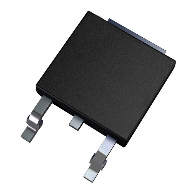
PPAK DPAK PENTAWATT TO-220 TO-220FP
Description
The LFxxAB/LFxxC are very Low Drop regulators available in PENTAWATT, TO-220, TO-220FP, DPAK and PPAK package and in a wide range of output voltages. The very Low Drop voltage (0.45V) and the very low quiescent current make them particularly suitable for Low Noise, Low Power applications and specially in battery powered systems.
In the 5 pins configuration (PENTAWATT and PPAK) a Shutdown Logic Control function is available (pin 2, TTL compatible). This means that when the device is used as a local regulator, it is possible to put a part of the board in standby, decreasing the total power consumption. In the three terminal configuration the device has the same electrical performance, but is fixed in the ON state. It requires only a 2.2 µF capacitor for stability allowing space and cost saving.
Table 1.
Device summary
Order codes LF15C LF15AB LF18C LF18AB LF25C LF25AB LF27C LF27AB LF30C LF30AB LF33C LF33AB LF35C LF35AB Rev. 18 LF40C LF40AB LF50C LF50AB LF60C LF60AB LF80C LF80AB LF85C LF85AB LF90C LF90AB LF120C LF120AB 1/45
www.st.com 45
July 2007
�LFxxAB - LFxxC
Contents
1 2 3 4 5 6 7 8 Diagram . . . . . . . . . . . . . . . . . . . . . . . . . . . . . . . . . . . . . . . . . . . . . . . . . . . 3 Pin configuration . . . . . . . . . . . . . . . . . . . . . . . . . . . . . . . . . . . . . . . . . . . 4 Maximum ratings . . . . . . . . . . . . . . . . . . . . . . . . . . . . . . . . . . . . . . . . . . . . 5 Electrical characteristics . . . . . . . . . . . . . . . . . . . . . . . . . . . . . . . . . . . . . 6 Typical performance characteristics . . . . . . . . . . . . . . . . . . . . . . . . . . . 32 Package mechanical data . . . . . . . . . . . . . . . . . . . . . . . . . . . . . . . . . . . . 36 Order codes . . . . . . . . . . . . . . . . . . . . . . . . . . . . . . . . . . . . . . . . . . . . . . 43
Revision history . . . . . . . . . . . . . . . . . . . . . . . . . . . . . . . . . . . . . . . . . . . 44
2/45
�LFxxAB - LFxxC
Diagram
1
Figure 1.
Diagram
Block diagram
3/45
�Pin configuration
LFxxAB - LFxxC
2
Figure 2.
Pin configuration
Pin connections (top view)
TO-220
TO-220FP
PPAK
DPAK
PENTAWATT
4/45
�LFxxAB - LFxxC
Maximum ratings
3
Table 2.
Maximum ratings
Absolute maximum ratings
Parameter DC input voltage Output current Power dissipation Storage temperature range Operating junction temperature range Value -0.5 to 40(1) Internally Limited Internally Limited -40 to 150 -40 to 125 °C °C Unit V
Symbol VI IO PTOT TSTG TOP
1. For 18 < VI < 40 the regulator is in shut-down
Table 3.
Symbol RthJC RthJA
Thermal data
Parameter Thermal resistance junction-case Thermal resistance junction-ambient PENTAWATT 3 50 TO-220 3 50 TO-220FP 5 60 DPAK/PPAK 8 100 Unit °C/W °C/W
Figure 3.
Test circuit
5/45
�Electrical characteristics
LFxxAB - LFxxC
4
Table 4.
Symbol VO VI IO ΔVO ΔVO
Electrical characteristics
Electrical characteristics for LF15AB (refer to the test circuits, TJ = 25°C, CI = 0.1 µF, CO = 2.2 μF unless otherwise specified.)
Parameter Output voltage Operating input voltage Output current limit Line regulation Load regulation VI = 2.5 to 16 V, IO = 5 mA VI = 2.8 V, IO = 5 to 500 mA VI = 2.5 to 16V, IO = 0mA Id Quiescent current VI = 2.8 to 16V, IO=500mA VI = 6 V OFF MODE f = 120 Hz SVR Supply voltage rejection IO = 5 mA, VI = 3.5 ± 1 V f = 1 KHz f = 10 KHz eN Vd VIL VIH II CO Output noise voltage Dropout voltage Control input logic low Control input logic high Control input current Output bypass capacitance B = 10 Hz to 100 KHz IO = 200 mA Ta = -40 to 125°C Ta = -40 to 125°C VI = 6 V, VC = 6 V ESR = 0.1 to 10 Ω IO = 0 to 500 mA , 2 2 10 10 50 82 77 65 50 1 0.8 µV V V V µA µF dB ON MODE 12 100 µA Test conditions IO = 50 mA, VI = 3.5 V IO = 50 mA, VI = 3.5 V, Ta = -25 to 85°C IO = 500 mA Min. 1.485 1.470 2.5 1 2 2 0.5 10 10 1 mA Typ. 1.5 Max. 1.515 V 1.530 16 V A mV mV Unit
6/45
�LFxxAB - LFxxC
Electrical characteristics
Table 5.
Symbol VO VI IO ΔVO ΔVO
Electrical characteristics for LF15C (refer to the test circuits, TJ = 25°C, CI = 0.1 µF, CO = 2.2 μF unless otherwise specified.)
Parameter Output voltage Operating input voltage Output current limit Line regulation Load regulation VI = 2.5 to 16 V, IO = 5 mA VI = 2.8 V, IO = 5 to 500 mA VI = 2.5 to 16V, IO = 0mA ON MODE 12 OFF MODE f = 120 Hz 50 82 77 65 50 1 0.8 2 10 2 10 µV V V V µA µF dB 100 µA Test conditions IO = 50 mA, VI = 3.5 V IO = 50 mA, VI = 3.5 V, Ta = -25 to 85°C IO = 500 mA Min. 1.47 1.44 2.5 1 2 2 0.5 10 10 1 mA Typ. 1.5 Max. 1.53 V 1.56 16 V A mV mV Unit
Id
Quiescent current
VI = 2.8 to 16V, IO=500mA VI = 6 V
SVR
Supply voltage rejection
IO = 5 mA, VI = 3.5 ± 1 V
f = 1 KHz f = 10 KHz
eN Vd VIL VIH II CO
Output noise voltage Dropout voltage Control input logic low Control input logic high Control input current Output bypass capacitance
B = 10 Hz to 100 KHz IO = 200 mA Ta = -40 to 125°C Ta = -40 to 125°C VI = 6 V, VC = 6 V ESR = 0.1 to 10 Ω IO = 0 to 500 mA ,
7/45
�Electrical characteristics
LFxxAB - LFxxC
Table 6.
Symbol VO VI IO ΔVO ΔVO
Electrical characteristics for LF18AB (refer to the test circuits, TJ = 25°C, CI = 0.1 µF, CO = 2.2 μF unless otherwise specified.)
Parameter Output voltage Operating input voltage Output current limit Line regulation Load regulation VI = 2.8 to 16 V, IO = 5 mA VI = 3.3 V, IO = 5 to 500 mA VI = 2.5 to 16V, IO = 0mA ON MODE 12 OFF MODE f = 120 Hz 50 82 77 60 50 0.7 0.8 2 10 2 10 µV V V V µA µF dB 100 µA Test conditions IO = 50 mA, VI = 3.3 V IO = 50 mA, VI = 3.3 V, Ta = -25 to 85°C IO = 500 mA Min. 1.782 1.764 3 1 2 2 0.5 12 10 1 mA Typ. 1.8 Max. 1.818 V 1.836 16 V A mV mV Unit
Id
Quiescent current
VI = 3.1 to 16V, IO=500mA VI = 6 V
SVR
Supply voltage rejection
IO = 5 mA, VI = 3.5 ± 1 V
f = 1 KHz f = 10 KHz
eN Vd VIL VIH II CO
Output noise voltage Dropout voltage Control input logic low Control input logic high Control input current Output bypass capacitance
B = 10 Hz to 100 KHz IO = 200 mA Ta = -40 to 125°C Ta = -40 to 125°C VI = 6 V, VC = 6 V ESR = 0.1 to 10 Ω IO = 0 to 500 mA ,
8/45
�LFxxAB - LFxxC
Electrical characteristics
Table 7.
Symbol VO VI IO ΔVO ΔVO
Electrical characteristics for LF18C (refer to the test circuits, TJ = 25°C, CI = 0.1 µF, CO = 2.2 μF unless otherwise specified.)
Parameter Output voltage Operating input voltage Output current limit Line regulation Load regulation VI = 2.8 to 16 V, IO = 5 mA VI = 3.3 V, IO = 5 to 500 mA VI = 2.5 to 16V, IO = 0mA ON MODE 12 OFF MODE f = 120 Hz 50 82 77 60 50 0.7 0.8 2 10 2 10 µV V V V µA µF dB 100 µA Test conditions IO = 50 mA, VI = 3.5 V IO = 50 mA, VI = 3.5 V, Ta = -25 to 85°C IO = 500 mA Min. 1.764 1.728 3 1 2 2 0.5 12 10 1 mA Typ. 1.8 Max. 1.836 V 1.872 16 V A mV mV Unit
Id
Quiescent current
VI = 3.1 to 16V, IO=500mA VI = 6 V
SVR
Supply voltage rejection
IO = 5 mA, VI = 3.5 ± 1 V
f = 1 KHz f = 10 KHz
eN Vd VIL VIH II CO
Output noise voltage Dropout voltage Control input logic low Control input logic high Control input current Output bypass capacitance
B = 10 Hz to 100 KHz IO = 200 mA Ta = -40 to 125°C Ta = -40 to 125°C VI = 6 V, VC = 6 V ESR = 0.1 to 10 Ω IO = 0 to 500 mA ,
9/45
�Electrical characteristics
LFxxAB - LFxxC
Table 8.
Symbol VO VI IO ΔVO ΔVO
Electrical characteristics for LF25AB (refer to the test circuits, TJ = 25°C, CI = 0.1 µF, CO = 2.2 μF unless otherwise specified.)
Parameter Output voltage Operating input voltage Output current limit Line regulation Load regulation VI = 3.5 to 16 V, IO = 5 mA VI = 3.8 V, IO = 5 to 500 mA VI = 3.5 to 16V, IO = 0mA ON MODE 12 OFF MODE f = 120 Hz 50 82 77 65 50 0.2 0.4 0.35 V 0.7 0.8 2 10 2 10 V V µA µF µV dB 100 µA Test conditions IO = 50 mA, VI = 4.5 V IO = 50 mA, VI = 4.5 V, Ta = -25 to 85°C IO = 500 mA 1 2 2 0.5 12 12 1 mA Min. 2.475 2.450 Typ. 2.5 Max. 2.525 V 2.550 16 V A mV mV Unit
Id
Quiescent current
VI = 3.8 to 16V, IO=500mA VI = 6 V
SVR
Supply voltage rejection
IO = 5 mA, VI = 4.5 ± 1 V
f = 1 KHz f = 10 KHz
eN Vd VIL VIH II CO
Output noise voltage Dropout voltage Control input logic low Control input logic high Control input current Output bypass capacitance
B = 10 Hz to 100 KHz IO = 200 mA IO = 500 mA Ta = -40 to 125°C Ta = -40 to 125°C VI = 6 V, VC = 6 V ESR = 0.1 to 10 Ω IO = 0 to 500 mA ,
10/45
�LFxxAB - LFxxC
Electrical characteristics
Table 9.
Symbol VO VI IO ΔVO ΔVO
Electrical characteristics for LF25C (refer to the test circuits, TJ = 25°C, CI = 0.1 µF, CO = 2.2 μF unless otherwise specified.)
Parameter Output voltage Operating input voltage Output current limit Line regulation Load regulation VI = 3.5 to 16 V, IO = 5 mA VI = 3.8 V, IO = 5 to 500 mA VI = 3.5 to 16V, IO = 0mA ON MODE 12 OFF MODE f = 120 Hz 50 82 77 65 50 0.2 0.4 0.35 V 0.7 0.8 2 10 2 10 V V µA µF µV dB 100 µA Test conditions IO = 50 mA, VI = 4.5 V IO = 50 mA, VI = 4.5 V, Ta = -25 to 85°C IO = 500 mA 1 2 2 0.5 12 12 1 mA Min. 2.45 2.4 Typ. 2.5 Max. 2.55 V 2.6 16 V A mV mV Unit
Id
Quiescent current
VI = 3.8 to 16V, IO=500mA VI = 6 V
SVR
Supply voltage rejection
IO = 5 mA, VI = 4.5 ± 1 V
f = 1 KHz f = 10 KHz
eN Vd VIL VIH II CO
Output noise voltage Dropout voltage Control input logic low Control input logic high Control input current Output bypass capacitance
B = 10 Hz to 100 KHz IO = 200 mA IO = 500 mA Ta = -40 to 125°C Ta = -40 to 125°C VI = 6 V, VC = 6 V ESR = 0.1 to 10 Ω IO = 0 to 500 mA ,
11/45
�Electrical characteristics
LFxxAB - LFxxC
Table 10.
Symbol VO VI IO ΔVO ΔVO
Electrical characteristics for LF27AB (refer to the test circuits, TJ = 25°C, CI = 0.1 µF, CO = 2.2 μF unless otherwise specified.)
Parameter Output voltage Operating input voltage Output current limit Line regulation Load regulation VI = 3.7 to 16 V, IO = 5 mA VI = 4 V, IO = 5 to 500 mA VI = 3.7 to 16V, IO = 0mA ON MODE 12 OFF MODE f = 120 Hz 50 82 77 65 50 0.2 0.4 0.35 V 0.7 0.8 2 10 2 10 V V µA µF µV dB 100 µA Test conditions IO = 50 mA, VI = 4.7 V IO = 50 mA, VI = 4.7 V, Ta = -25 to 85°C IO = 500 mA 1 2 2 0.5 13 13 1 mA Min. 2.673 2.646 Typ. 2.7 Max. 2.727 V 2.754 16 V A mV mV Unit
Id
Quiescent current
VI = 4 to 16V, IO = 500mA VI = 6 V
SVR
Supply voltage rejection
IO = 5 mA, VI = 4.7 ± 1 V
f = 1 KHz f = 10 KHz
eN Vd VIL VIH II CO
Output noise voltage Dropout voltage Control input logic low Control input logic high Control input current Output bypass capacitance
B = 10 Hz to 100 KHz IO = 200 mA IO = 500 mA Ta = -40 to 125°C Ta = -40 to 125°C VI = 6 V, VC = 6 V ESR = 0.1 to 10 Ω IO = 0 to 500 mA ,
12/45
�LFxxAB - LFxxC
Electrical characteristics
Table 11.
Symbol VO VI IO ΔVO ΔVO
Electrical characteristics for LF27C (refer to the test circuits, TJ = 25°C, CI = 0.1 µF, CO = 2.2 μF unless otherwise specified.)
Parameter Output voltage Operating input voltage Output current limit Line regulation Load regulation VI = 3.7 to 16 V, IO = 5 mA VI = 4 V, IO = 5 to 500 mA VI = 3.7 to 16V, IO = 0mA ON MODE 12 OFF MODE f = 120 Hz 50 82 77 65 50 0.2 0.4 0.35 V 0.7 0.8 2 10 2 10 V V µA µF µV dB 100 µA Test conditions IO = 50 mA, VI = 4.7 V IO = 50 mA, VI = 4.7 V, Ta = -25 to 85°C IO = 500 mA 1 2 2 0.5 13 13 1 mA Min. 2.646 2.592 Typ. 2.7 Max. 2.754 V 2.808 16 V A mV mV Unit
Id
Quiescent current
VI = 4 to 16V, IO = 500mA VI = 6 V
SVR
Supply voltage rejection
IO = 5 mA, VI = 4.7 ± 1 V
f = 1 KHz f = 10 KHz
eN Vd VIL VIH II CO
Output noise voltage Dropout voltage Control input logic low Control input logic high Control input current Output bypass capacitance
B = 10 Hz to 100 KHz IO = 200 mA IO = 500 mA Ta = -40 to 125°C Ta = -40 to 125°C VI = 6 V, VC = 6 V ESR = 0.1 to 10 Ω IO = 0 to 500 mA ,
13/45
�Electrical characteristics
LFxxAB - LFxxC
Table 12.
Symbol VO VI IO ΔVO ΔVO
Electrical characteristics for LF30AB (refer to the test circuits, TJ = 25°C, CI = 0.1 µF, CO = 2.2 μF unless otherwise specified.)
Parameter Output voltage Operating input voltage Output current limit Line regulation Load regulation VI = 4 to 16 V, IO = 5 mA VI = 4.3 V, IO = 5 to 500 mA VI = 4 to 16V, IO = 0mA ON MODE 12 OFF MODE f = 120 Hz 50 81 76 65 50 0.2 0.4 0.35 V 0.7 0.8 2 10 2 10 V V µA µF µV dB 100 µA Test conditions IO = 50 mA, VI = 5 V IO = 50 mA, VI = 5 V, Ta = -25 to 85°C IO = 500 mA 1 3 3 0.5 15 15 1 mA Min. 2.970 2.94 Typ. 3 Max. 3.03 V 3.06 16 V A mV mV Unit
Id
Quiescent current
VI = 4.3 to 16V, IO=500mA VI = 6 V
SVR
Supply voltage rejection
IO = 5 mA, VI = 5 ± 1 V
f = 1 KHz f = 10 KHz
eN Vd VIL VIH II CO
Output noise voltage Dropout voltage Control input logic low Control input logic high Control input current Output bypass capacitance
B = 10 Hz to 100 KHz IO = 200 mA IO = 500 mA Ta = -40 to 125°C Ta = -40 to 125°C VI = 6 V, VC = 6 V ESR = 0.1 to 10 Ω IO = 0 to 500 mA ,
14/45
�LFxxAB - LFxxC
Electrical characteristics
Table 13.
Symbol VO VI IO ΔVO ΔVO
Electrical characteristics for LF30C (refer to the test circuits, TJ = 25°C, CI = 0.1 µF, CO = 2.2 μF unless otherwise specified.)
Parameter Output voltage Operating input voltage Output current limit Line regulation Load regulation VI = 4 to 16 V, IO = 5 mA VI = 4.3 V, IO = 5 to 500 mA VI = 4 to 16V, IO = 0mA ON MODE 12 OFF MODE f = 120 Hz 50 81 76 65 50 0.2 0.4 0.35 V 0.7 0.8 2 10 2 10 V V µA µF µV dB 100 µA Test conditions IO = 50 mA, VI = 5 V IO = 50 mA, VI = 5 V, Ta = -25 to 85°C IO = 500 mA 1 3 3 0.5 15 15 1 mA Min. 2.94 2.88 Typ. 3 Max. 3.06 V 3.12 16 V A mV mV Unit
Id
Quiescent current
VI = 4.3 to 16V, IO=500mA VI = 6 V
SVR
Supply voltage rejection
IO = 5 mA, VI = 5 ± 1 V
f = 1 KHz f = 10 KHz
eN Vd VIL VIH II CO
Output noise voltage Dropout voltage Control input logic low Control input logic high Control input current Output bypass capacitance
B = 10 Hz to 100 KHz IO = 200 mA IO = 500 mA Ta = -40 to 125°C Ta = -40 to 125°C VI = 6 V, VC = 6 V ESR = 0.1 to 10 Ω IO = 0 to 500 mA ,
15/45
�Electrical characteristics
LFxxAB - LFxxC
Table 14.
Symbol VO VI IO ΔVO ΔVO
Electrical characteristics for LF33AB (refer to the test circuits, TJ = 25°C, CI = 0.1 µF, CO = 2.2 μF unless otherwise specified.)
Parameter Output voltage Operating input voltage Output current limit Line regulation Load regulation VI = 4.3 to 16 V, IO = 5 mA VI = 4.6 V, IO = 5 to 500 mA VI = 4.3 to 16V, IO = 0mA ON MODE 12 OFF MODE f = 120 Hz 50 80 75 65 50 0.2 0.4 0.35 V 0.7 0.8 2 10 2 10 V V µA µF µV dB 100 µA Test conditions IO = 50 mA, VI = 5.3 V IO = 50 mA, VI = 5.3 V, Ta = -25 to 85°C IO = 500 mA 1 3 3 0.5 16 16 1 mA Min. 3.267 3.234 Typ. 3.3 Max. 3.333 V 3.366 16 V A mV mV Unit
Id
Quiescent current
VI = 4.6 to 16V, IO=500mA VI = 6 V
SVR
Supply voltage rejection
IO = 5 mA, VI = 5.3 ± 1 V
f = 1 KHz f = 10 KHz
eN Vd VIL VIH II CO
Output noise voltage Dropout voltage Control input logic low Control input logic high Control input current Output bypass capacitance
B = 10 Hz to 100 KHz IO = 200 mA IO = 500 mA Ta = -40 to 125°C Ta = -40 to 125°C VI = 6 V, VC = 6 V ESR = 0.1 to 10 Ω IO = 0 to 500 mA ,
16/45
�LFxxAB - LFxxC
Electrical characteristics
Table 15.
Symbol VO VI IO ΔVO ΔVO
Electrical characteristics for LF33C (refer to the test circuits, TJ = 25°C, CI = 0.1 µF, CO = 2.2 μF unless otherwise specified.)
Parameter Output voltage Operating input voltage Output current limit Line regulation Load regulation VI = 4.3 to 16 V, IO = 5 mA VI = 4.6 V, IO = 5 to 500 mA VI = 4.3 to 16V, IO = 0mA ON MODE 12 OFF MODE f = 120 Hz 50 80 75 65 50 0.2 0.4 0.35 V 0.7 0.8 2 10 2 10 V V µA µF µV dB 100 µA Test conditions IO = 50 mA, VI = 5.3 V IO = 50 mA, VI = 5.3 V, Ta = -25 to 85°C IO = 500 mA 1 3 3 0.5 16 16 1 mA Min. 3.234 3.168 Typ. 3.3 Max. 3.366 V 3.432 16 V A mV mV Unit
Id
Quiescent current
VI = 4.6 to 16V, IO=500mA VI = 6 V
SVR
Supply voltage rejection
IO = 5 mA, VI = 5.3 ± 1 V
f = 1 KHz f = 10 KHz
eN Vd VIL VIH II CO
Output noise voltage Dropout voltage Control input logic low Control input logic high Control input current Output bypass capacitance
B = 10 Hz to 100 KHz IO = 200 mA IO = 500 mA Ta = -40 to 125°C Ta = -40 to 125°C VI = 6 V, VC = 6 V ESR = 0.1 to 10 Ω IO = 0 to 500 mA ,
17/45
�Electrical characteristics
LFxxAB - LFxxC
Table 16.
Symbol VO VI IO ΔVO ΔVO
Electrical characteristics for LF35AB (refer to the test circuits, TJ = 25°C, CI = 0.1 µF, CO = 2.2 μF unless otherwise specified.)
Parameter Output voltage Operating input voltage Output current limit Line regulation Load regulation VI = 4.5 to 16 V, IO = 5 mA VI = 4.8 V, IO = 5 to 500 mA VI = 4.5 to 16V, IO = 0mA ON MODE 12 OFF MODE f = 120 Hz 50 79 74 60 50 0.2 0.4 0.35 V 0.7 0.8 2 10 2 10 V V µA µF µV dB 100 µA Test conditions IO = 50 mA, VI = 5.5 V IO = 50 mA, VI = 5.5 V, Ta = -25 to 85°C IO = 500 mA 1 3 3 0.5 17 17 1 mA Min. 3.465 3.430 Typ. 3.5 Max. 3.535 V 3.570 16 V A mV mV Unit
Id
Quiescent current
VI = 4.8 to 16V, IO=500mA VI = 6 V
SVR
Supply voltage rejection
IO = 5 mA, VI = 5.5 ± 1 V
f = 1 KHz f = 10 KHz
eN Vd VIL VIH II CO
Output noise voltage Dropout voltage Control input logic low Control input logic high Control input current Output bypass capacitance
B = 10 Hz to 100 KHz IO = 200 mA IO = 500 mA Ta = -40 to 125°C Ta = -40 to 125°C VI = 6 V, VC = 6 V ESR = 0.1 to 10 Ω IO = 0 to 500 mA ,
18/45
�LFxxAB - LFxxC
Electrical characteristics
Table 17.
Symbol VO VI IO ΔVO ΔVO
Electrical characteristics for LF35C (refer to the test circuits, TJ = 25°C, CI = 0.1 µF, CO = 2.2 μF unless otherwise specified.)
Parameter Output voltage Operating input voltage Output current limit Line regulation Load regulation VI = 4.5 to 16 V, IO = 5 mA VI = 4.8 V, IO = 5 to 500 mA VI = 4.5 to 16V, IO = 0mA ON MODE 12 OFF MODE f = 120 Hz 50 79 74 60 50 0.2 0.4 0.35 V 0.7 0.8 2 10 2 10 V V µA µF µV dB 100 µA Test conditions IO = 50 mA, VI = 5.5 V IO = 50 mA, VI = 5.5 V, Ta = -25 to 85°C IO = 500 mA 1 3 3 0.5 17 17 1 mA Min. 3.43 3.36 Typ. 3.5 Max. 3.57 V 3.64 16 V A mV mV Unit
Id
Quiescent current
VI = 4.8 to 16V, IO=500mA VI = 6 V
SVR
Supply voltage rejection
IO = 5 mA, VI = 5.5 ± 1 V
f = 1 KHz f = 10 KHz
eN Vd VIL VIH II CO
Output noise voltage Dropout voltage Control input logic low Control input logic high Control input current Output bypass capacitance
B = 10 Hz to 100 KHz IO = 200 mA IO = 500 mA Ta = -40 to 125°C Ta = -40 to 125°C VI = 6 V, VC = 6 V ESR = 0.1 to 10 Ω IO = 0 to 500 mA ,
19/45
�Electrical characteristics
LFxxAB - LFxxC
Table 18.
Symbol VO VI IO ΔVO ΔVO
Electrical characteristics for LF50AB (refer to the test circuits, TJ = 25°C, CI = 0.1 µF, CO = 2.2 μF unless otherwise specified.)
Parameter Output voltage Operating input voltage Output current limit Line regulation Load regulation VI = 6 to 16 V, IO = 5 mA VI = 6.3 V, IO = 5 to 500 mA VI = 6 to 16V, IO = 0mA ON MODE 12 OFF MODE f = 120 Hz 50 76 71 60 50 0.2 0.4 0.35 V 0.7 0.8 2 10 2 10 V V µA µF µV dB 100 µA Test conditions IO = 50 mA, VI = 7 V IO = 50 mA, VI = 7 V, Ta = -25 to 85°C IO = 500 mA 1 5 5 0.5 25 25 1 mA Min. 4.95 4.9 Typ. 5 Max. 5.05 V 5.1 16 V A mV mV Unit
Id
Quiescent current
VI = 6.3 to 16V, IO=500mA VI = 6 V
SVR
Supply voltage rejection
IO = 5 mA, VI = 7 ± 1 V
f = 1 KHz f = 10 KHz
eN Vd VIL VIH II CO
Output noise voltage Dropout voltage Control input logic low Control input logic high Control input current Output bypass capacitance
B = 10 Hz to 100 KHz IO = 200 mA IO = 500 mA Ta = -40 to 125°C Ta = -40 to 125°C VI = 6 V, VC = 6 V ESR = 0.1 to 10 Ω IO = 0 to 500 mA ,
20/45
�LFxxAB - LFxxC
Electrical characteristics
Table 19.
Symbol VO VI IO ΔVO ΔVO
Electrical characteristics for LF50C (refer to the test circuits, TJ = 25°C, CI = 0.1 µF, CO = 2.2 μF unless otherwise specified.)
Parameter Output voltage Operating input voltage Output current limit Line regulation Load regulation VI = 6 to 16 V, IO = 5 mA VI = 6.3 V, IO = 5 to 500 mA VI = 6 to 16V, IO = 0mA ON MODE 12 OFF MODE f = 120 Hz 50 76 71 60 50 0.2 0.4 0.35 V 0.7 0.8 2 10 2 10 V V µA µF µV dB 100 µA Test conditions IO = 50 mA, VI = 7 V IO = 50 mA, VI = 7 V, Ta = -25 to 85°C IO = 500 mA 1 5 5 0.5 25 25 1 mA Min. 4.9 4.8 Typ. 5 Max. 5.1 V 5.2 16 V A mV mV Unit
Id
Quiescent current
VI = 6.3 to 16V, IO=500mA VI = 6 V
SVR
Supply voltage rejection
IO = 5 mA, VI = 7 ± 1 V
f = 1 KHz f = 10 KHz
eN Vd VIL VIH II CO
Output noise voltage Dropout voltage Control input logic low Control input logic high Control input current Output bypass capacitance
B = 10 Hz to 100 KHz IO = 200 mA IO = 500 mA Ta = -40 to 125°C Ta = -40 to 125°C VI = 6 V, VC = 6 V ESR = 0.1 to 10 Ω IO = 0 to 500 mA ,
21/45
�Electrical characteristics
LFxxAB - LFxxC
Table 20.
Symbol VO VI IO ΔVO ΔVO
Electrical characteristics for LF60AB (refer to the test circuits, TJ = 25°C, CI = 0.1 µF, CO = 2.2 μF unless otherwise specified.)
Parameter Output voltage Operating input voltage Output current limit Line regulation Load regulation VI = 7 to 16 V, IO = 5 mA VI = 7.3 V, IO = 5 to 500 mA VI = 7 to 16V, IO = 0mA ON MODE 12 OFF MODE f = 120 Hz 70 75 70 60 50 0.2 0.4 0.35 V 0.7 0.8 2 10 2 10 V V µA µF µV dB 140 µA Test conditions IO = 50 mA, VI = 8 V IO = 50 mA, VI = 8 V, Ta = -25 to 85°C IO = 500 mA 1 6 6 0.7 30 30 1.5 mA Min. 5.94 5.88 Typ. 6 Max. 6.06 V 6.12 16 V A mV mV Unit
Id
Quiescent current
VI = 7.3 to 16V, IO=500mA VI = 9 V
SVR
Supply voltage rejection
IO = 5 mA, VI = 8 ± 1 V
f = 1 KHz f = 10 KHz
eN Vd VIL VIH II CO
Output noise voltage Dropout voltage Control input logic low Control input logic high Control input current Output bypass capacitance
B = 10 Hz to 100 KHz IO = 200 mA IO = 500 mA Ta = -40 to 125°C Ta = -40 to 125°C VI = 9 V, VC = 6 V ESR = 0.1 to 10 Ω IO = 0 to 500 mA ,
22/45
�LFxxAB - LFxxC
Electrical characteristics
Table 21.
Symbol VO VI IO ΔVO ΔVO
Electrical characteristics for LF60C (refer to the test circuits, TJ = 25°C, CI = 0.1 µF, CO = 2.2 μF unless otherwise specified.)
Parameter Output voltage Operating input voltage Output current limit Line regulation Load regulation VI = 7 to 16 V, IO = 5 mA VI = 7.3 V, IO = 5 to 500 mA VI = 7 to 16V, IO = 0mA ON MODE 12 OFF MODE f = 120 Hz 70 75 70 60 50 0.2 0.4 0.35 V 0.7 0.8 2 10 2 10 V V µA µF µV dB 140 µA Test conditions IO = 50 mA, VI = 8 V IO = 50 mA, VI = 8 V, Ta = -25 to 85°C IO = 500 mA 1 6 6 0.7 30 30 1.5 mA Min. 5.88 5.76 Typ. 6 Max. 6.12 V 6.24 16 V A mV mV Unit
Id
Quiescent current
VI = 7.3 to 16V, IO=500mA VI = 9 V
SVR
Supply voltage rejection
IO = 5 mA, VI = 8 ± 1 V
f = 1 KHz f = 10 KHz
eN Vd VIL VIH II CO
Output noise voltage Dropout voltage Control input logic low Control input logic high Control input current Output bypass capacitance
B = 10 Hz to 100 KHz IO = 200 mA IO = 500 mA Ta = -40 to 125°C Ta = -40 to 125°C VI = 9 V, VC = 6 V ESR = 0.1 to 10 Ω IO = 0 to 500 mA ,
23/45
�Electrical characteristics
LFxxAB - LFxxC
Table 22.
Symbol VO VI IO ΔVO ΔVO
Electrical characteristics for LF80AB (refer to the test circuits, TJ = 25°C, CI = 0.1 µF, CO = 2.2 μF unless otherwise specified.)
Parameter Output voltage Operating input voltage Output current limit Line regulation Load regulation VI = 9 to 16 V, IO = 5 mA VI = 9.3 V, IO = 5 to 500 mA VI = 9 to 16V, IO = 0mA ON MODE 12 OFF MODE f = 120 Hz 70 72 67 57 50 0.2 0.4 0.35 V 0.7 0.8 2 10 2 10 V V µA µF µV dB 140 µA Test conditions IO = 50 mA, VI = 10 V IO = 50 mA, VI = 10 V, Ta = -25 to 85°C IO = 500 mA 1 8 8 0.7 40 40 1.5 mA Min. 7.92 7.84 Typ. 8 Max. 8.08 V 8.16 16 V A mV mV Unit
Id
Quiescent current
VI = 9.3 to 16V, IO=500mA VI = 9 V
SVR
Supply voltage rejection
IO = 5 mA, VI = 10 ± 1 V
f = 1 KHz f = 10 KHz
eN Vd VIL VIH II CO
Output noise voltage Dropout voltage Control input logic low Control input logic high Control input current Output bypass capacitance
B = 10 Hz to 100 KHz IO = 200 mA IO = 500 mA Ta = -40 to 125°C Ta = -40 to 125°C VI = 9 V, VC = 6 V ESR = 0.1 to 10 Ω IO = 0 to 500 mA ,
24/45
�LFxxAB - LFxxC
Electrical characteristics
Table 23.
Symbol VO VI IO ΔVO ΔVO
Electrical characteristics for LF80C (refer to the test circuits, TJ = 25°C, CI = 0.1 µF, CO = 2.2 μF unless otherwise specified.)
Parameter Output voltage Operating input voltage Output current limit Line regulation Load regulation VI = 9 to 16 V, IO = 5 mA VI = 9.3 V, IO = 5 to 500 mA VI = 9 to 16V, IO = 0mA ON MODE 12 OFF MODE f = 120 Hz 70 72 67 57 50 0.2 0.4 0.35 V 0.7 0.8 2 10 2 10 V V µA µF µV dB 140 µA Test conditions IO = 50 mA, VI = 10 V IO = 50 mA, VI = 10 V, Ta = -25 to 85°C IO = 500 mA 1 8 8 0.7 40 40 1.5 mA Min. 7.84 7.68 Typ. 8 Max. 8.16 V 8.32 16 V A mV mV Unit
Id
Quiescent current
VI = 9.3 to 16V, IO=500mA VI = 9 V
SVR
Supply voltage rejection
IO = 5 mA, VI = 10 ± 1 V
f = 1 KHz f = 10 KHz
eN Vd VIL VIH II CO
Output noise voltage Dropout voltage Control input logic low Control input logic high Control input current Output bypass capacitance
B = 10 Hz to 100 KHz IO = 200 mA IO = 500 mA Ta = -40 to 125°C Ta = -40 to 125°C VI = 9 V, VC = 6 V ESR = 0.1 to 10 Ω IO = 0 to 500 mA ,
25/45
�Electrical characteristics
LFxxAB - LFxxC
Table 24.
Symbol VO VI IO ΔVO ΔVO
Electrical characteristics for LF85AB (refer to the test circuits, TJ = 25°C, CI = 0.1 µF, CO = 2.2 μF unless otherwise specified.)
Parameter Output voltage Operating input voltage Output current limit Line regulation Load regulation VI = 9.5 to 16 V, IO = 5 mA VI = 9.8 V, IO = 5 to 500 mA VI = 9.5 to 16V, IO = 0mA ON MODE 12 OFF MODE f = 120 Hz 70 72 67 57 50 0.2 0.4 0.35 V 0.7 0.8 2 10 2 10 V V µA µF µV dB 140 µA Test conditions IO = 50 mA, VI = 10.5 V IO = 50 mA, VI = 10.5 V, Ta = -25 to 85°C IO = 500 mA 1 8 8 0.7 42 42 1.5 mA Min. 8.415 8.33 Typ. 8.5 Max. 8.585 V 8.67 16 V A mV mV Unit
Id
Quiescent current
VI = 9.8 to 16V, IO=500mA VI = 9 V
SVR
Supply voltage rejection
IO = 5 mA, VI = 10.5 ± 1 V
f = 1 KHz f = 10 KHz
eN Vd VIL VIH II CO
Output noise voltage Dropout voltage Control input logic low Control input logic high Control input current Output bypass capacitance
B = 10 Hz to 100 KHz IO = 200 mA IO = 500 mA Ta = -40 to 125°C Ta = -40 to 125°C VI = 9 V, VC = 6 V ESR = 0.1 to 10 Ω IO = 0 to 500 mA ,
26/45
�LFxxAB - LFxxC
Electrical characteristics
Table 25.
Symbol VO VI IO ΔVO ΔVO
Electrical characteristics for LF85C (refer to the test circuits, TJ = 25°C, CI = 0.1 µF, CO = 2.2 μF unless otherwise specified.)
Parameter Output voltage Operating input voltage Output current limit Line regulation Load regulation VI = 9.5 to 16 V, IO = 5 mA VI = 9.8 V, IO = 5 to 500 mA VI = 9.5 to 16V, IO = 0mA ON MODE 12 OFF MODE f = 120 Hz 70 72 67 57 50 0.2 0.4 0.35 V 0.7 0.8 2 10 2 10 V V µA µF µV dB 140 µA Test conditions IO = 50 mA, VI = 10.5 V IO = 50 mA, VI = 10.5 V, Ta = -25 to 85°C IO = 500 mA 1 8 8 0.7 42 42 1.5 mA Min. 8.33 8.16 Typ. 8.5 Max. 8.67 V 8.84 16 V A mV mV Unit
Id
Quiescent current
VI = 9.8 to 16V, IO=500mA VI = 9 V
SVR
Supply voltage rejection
IO = 5 mA, VI = 10.5 ± 1 V
f = 1 KHz f = 10 KHz
eN Vd VIL VIH II CO
Output noise voltage Dropout voltage Control input logic low Control input logic high Control input current Output bypass capacitance
B = 10 Hz to 100 KHz IO = 200 mA IO = 500 mA Ta = -40 to 125°C Ta = -40 to 125°C VI = 9 V, VC = 6 V ESR = 0.1 to 10 Ω IO = 0 to 500 mA ,
27/45
�Electrical characteristics
LFxxAB - LFxxC
Table 26.
Symbol VO VI IO ΔVO ΔVO
Electrical characteristics for LF90AB (refer to the test circuits, TJ = 25°C, CI = 0.1 µF, CO = 2.2 μF unless otherwise specified.)
Parameter Output voltage Operating input voltage Output current limit Line regulation Load regulation VI = 10 to 16 V, IO = 5 mA VI = 10.3 V, IO = 5 to 500 mA VI = 10 to 16V, IO = 0mA ON MODE 12 OFF MODE f = 120 Hz 70 71 66 56 50 0.2 0.4 0.35 V 0.7 0.8 2 10 2 10 V V µA µF µV dB 140 µA Test conditions IO = 50 mA, VI = 11 V IO = 50 mA, VI = 11 V, Ta = -25 to 85°C IO = 500 mA 1 9 9 0.7 45 45 1.5 mA Min. 8.91 8.82 Typ. 9 Max. 9.09 V 9.18 16 V A mV mV Unit
Id
Quiescent current
VI = 10.3 to 16V, IO = 500mA VI = 10 V
SVR
Supply voltage rejection
IO = 5 mA, VI = 11 ± 1 V
f = 1 KHz f = 10 KHz
eN Vd VIL VIH II CO
Output noise voltage Dropout voltage Control input logic low Control input logic high Control input current Output bypass capacitance
B = 10 Hz to 100 KHz IO = 200 mA IO = 500 mA Ta = -40 to 125°C Ta = -40 to 125°C VI = 10 V, VC = 6 V ESR = 0.1 to 10 Ω IO = 0 to 500 mA ,
28/45
�LFxxAB - LFxxC
Electrical characteristics
Table 27.
Symbol VO VI IO ΔVO ΔVO
Electrical characteristics for LF90C (refer to the test circuits, TJ = 25°C, CI = 0.1 µF, CO = 2.2 μF unless otherwise specified.)
Parameter Output voltage Operating input voltage Output current limit Line regulation Load regulation VI = 10 to 16 V, IO = 5 mA VI = 10.3 V, IO = 5 to 500 mA VI = 10 to 16V, IO = 0mA ON MODE 12 OFF MODE f = 120 Hz 70 71 66 56 50 0.2 0.4 0.35 V 0.7 0.8 2 10 2 10 V V µA µF µV dB 140 µA Test conditions IO = 50 mA, VI = 11 V IO = 50 mA, VI = 11 V, Ta = -25 to 85°C IO = 500 mA 1 9 9 0.7 45 45 1.5 mA Min. 8.82 8.64 Typ. 9 Max. 9.18 V 9.36 16 V A mV mV Unit
Id
Quiescent current
VI = 10.3 to 16V, IO = 500mA VI = 10 V
SVR
Supply voltage rejection
IO = 5 mA, VI = 11 ± 1 V
f = 1 KHz f = 10 KHz
eN Vd VIL VIH II CO
Output noise voltage Dropout voltage Control input logic low Control input logic high Control input current Output bypass capacitance
B = 10 Hz to 100 KHz IO = 200 mA IO = 500 mA Ta = -40 to 125°C Ta = -40 to 125°C VI = 10 V, VC = 6 V ESR = 0.1 to 10 Ω IO = 0 to 500 mA ,
29/45
�Electrical characteristics
LFxxAB - LFxxC
Table 28.
Symbol VO VI IO ΔVO ΔVO
Electrical characteristics for LF120AB (refer to the test circuits, TJ = 25°C, CI = 0.1 µF, CO = 2.2 μF unless otherwise specified.)
Parameter Output voltage Operating input voltage Output current limit Line regulation Load regulation VI = 13 to 16 V, IO = 5 mA VI = 13.3 V, IO = 5 to 500 mA VI = 13 to 16V, IO = 0mA ON MODE 12 OFF MODE f = 120 Hz 70 69 64 54 50 0.2 0.4 0.35 V 0.7 0.8 2 10 2 10 V V µA µF µV dB 140 µA Test conditions IO = 50 mA, VI = 15 V IO = 50 mA, VI = 15 V, Ta = -25 to 85°C IO = 500 mA 1 12 12 0.7 60 60 1.5 mA Min. 11.88 11.76 Typ. 12 Max. 12.12 V 12.24 16 V A mV mV Unit
Id
Quiescent current
VI = 13.3 to 16V, IO = 500mA VI = 13 V
SVR
Supply voltage rejection
IO = 5 mA, VI = 14 ± 1 V
f = 1 KHz f = 10 KHz
eN Vd VIL VIH II CO
Output noise voltage Dropout voltage Control input logic low Control input logic high Control input current Output bypass capacitance
B = 10 Hz to 100 KHz IO = 200 mA IO = 500 mA Ta = -40 to 125°C Ta = -40 to 125°C VI = 13 V, VC = 6 V ESR = 0.1 to 10 Ω IO = 0 to 500 mA ,
30/45
�LFxxAB - LFxxC
Electrical characteristics
Table 29.
Symbol VO VI IO ΔVO ΔVO
Electrical characteristics for LF120C (refer to the test circuits, TJ = 25°C, CI = 0.1 µF, CO = 2.2 μF unless otherwise specified).
Parameter Output voltage Operating input voltage Output current limit Line regulation Load regulation VI = 13 to 16 V, IO = 5 mA VI = 13.3 V, IO = 5 to 500 mA VI = 13 to 16V, IO = 0mA ON MODE 12 OFF MODE f = 120 Hz 70 69 64 54 50 0.2 0.4 0.35 V 0.7 0.8 2 10 2 10 V V µA µF µV dB 140 µA Test conditions IO = 50 mA, VI = 14 V IO = 50 mA, VI = 14 V, Ta = -25 to 85°C IO = 500 mA 1 12 12 0.7 60 60 1.5 mA Min. 11.76 11.52 Typ. 12 Max. 12.24 V 12.48 16 V A mV mV Unit
Id
Quiescent current
VI = 13.3 to 16V, IO = 500mA VI = 13 V
SVR
Supply voltage rejection
IO = 5 mA, VI = 14 ± 1 V
f = 1 KHz f = 10 KHz
eN Vd VIL VIH II CO
Output noise voltage Dropout voltage Control input logic low Control input logic high Control input current Output bypass capacitance
B = 10 Hz to 100 KHz IO = 200 mA IO = 500 mA Ta = -40 to 125°C Ta = -40 to 125°C VI = 13 V, VC = 6 V ESR = 0.1 to 10 Ω IO = 0 to 500 mA ,
31/45
�Typical performance characteristics
LFxxAB - LFxxC
5
Figure 4.
Typical performance characteristics
(unless otherwise specified VO(NOM) = 3.3 V) Dropout voltage vs output current Figure 5. Dropout voltage vs temperature
Figure 6.
Supply current vs input voltage
Figure 7.
Supply current vs input voltage
Figure 8.
Short circuit current vs input voltage
Figure 9.
Supply current vs temperature
32/45
�LFxxAB - LFxxC
Typical performance characteristics
Figure 10. Logic controlled precision 3.3/5.0v selectable output
Figure 11. Sequential multi-output supply
33/45
�Typical performance characteristics
LFxxAB - LFxxC
Figure 12. Multiple supply with ON/OFF toggle switch
Figure 13. Basic inhibit functions
34/45
�LFxxAB - LFxxC
Typical performance characteristics
Figure 14. Delayed Turn-On
Figure 15. Low voltage bulb blinker
35/45
�Package mechanical data
LFxxAB - LFxxC
6
Package mechanical data
In order to meet environmental requirements, ST offers these devices in ECOPACK® packages. These packages have a Lead-free second level interconnect. The category of second Level Interconnect is marked on the package and on the inner box label, in compliance with JEDEC Standard JESD97. The maximum ratings related to soldering conditions are also marked on the inner box label. ECOPACK is an ST trademark. ECOPACK specifications are available at: www.st.com.
36/45
�LFxxAB - LFxxC
Package mechanical data
PENTAWATT (Vertical) mechanical data
Dim. A C D D1 E F F1 G G1 H2 H3 L L1 L2 L3 L5 L6 L7 M M1 Dia1 Min. mm. Typ. Max. 4.8 1.37 2.8 1.35 0.55 1.05 1.4 3.6 7 10.4 10.4 Min. inch. Typ. Max. 0.189 0.054 0.110 0.053 0.022 0.041 0.055 0.142 0.276 0.409 0.409
2.4 1.2 0.35 0.8 1 3.2 6.6 10.05
3.4 6.8
0.094 0.047 0.014 0.031 0.039 0.126 0.260 0.396
0.134 0.268
17.85 15.75 21.4 22.5 2.6 15.1 6 4.5 4 3.65 3.85 0.144 3 15.8 6.6 0.102 0.594 0.236
0.703 0.620 0.843 0.886 0.118 0.622 0.260 0.177 0.157 0.152
P010E
37/45
�Package mechanical data
LFxxAB - LFxxC
TO-220 mechanical data
Dim. A C D D1 E F F1 F2 G G1 H2 L2 L4 L5 L6 L7 L9 DIA. 13.0 2.65 15.25 6.2 3.5 3.75 0.49 0.61 1.14 1.14 4.95 2.4 10.0 16.4 14.0 2.95 15.75 6.6 3.93 3.85 0.511 0.104 0.600 0.244 0.137 0.147 mm. Min. 4.40 1.23 2.40 1.27 0.70 0.88 1.70 1.70 5.15 2.7 10.40 0.019 0.024 0.044 0.044 0.194 0.094 0.393 0.645 0.551 0.116 0.620 0.260 0.154 0.151 Typ. Max. 4.60 1.32 2.72 Min. 0.173 0.048 0.094 0.050 0.027 0.034 0.067 0.067 0.203 0.106 0.409 inch. Typ. Max. 0.181 0.051 0.107
P011C
38/45
�LFxxAB - LFxxC
Package mechanical data
TO-220FP mechanical data
Dim. A B D E F F1 F2 G G1 H L2 L3 L4 L5 L6 L7 DIA. 28.6 9.8 2.9 15.9 9 3 mm. Min. 4.40 2.5 2.5 0.45 0.75 1.15 1.15 4.95 2.4 10.0 16 30.6 10.6 3.6 16.4 9.3 3.2 1.126 0.385 0.114 0.626 0.354 0.118 Typ Max. 4.60 2.7 2.75 0.70 1 1.50 1.50 5.2 2.7 10.40 Min. 0.173 0.098 0.098 0.017 0.030 0.045 0.045 0.194 0.094 0.393 0.630 1.204 0.417 0.142 0.645 0.366 0.126 inch. Typ. Max. 0.181 0.106 0.108 0.027 0.039 0.059 0.059 0.204 0.106 0.409
7012510A-H
39/45
�Package mechanical data
LFxxAB - LFxxC
DPAK mechanical data
mm. Dim. Min. A A1 A2 B b4 C C2 D D1 E E1 e e1 H L (L1) L2 L4 R V2 2.2 0.9 0.03 0.64 5.2 0.45 0.48 6 5.1 6.4 4.7 2.28 4.4 9.35 1 2.8 0.8 0.6 0.2 0° 8° 0° 1 0.023 0.008 8° 4.6 10.1 0.173 0.368 0.039 0.110 0.031 0.039 6.6 0.252 0.185 0.090 0.181 0.397 Typ. Max. 2.4 1.1 0.23 0.9 5.4 0.6 0.6 6.2 Min. 0.086 0.035 0.001 0.025 0.204 0.017 0.019 0.236 0.200 0.260 Typ. Max. 0.094 0.043 0.009 0.035 0.212 0.023 0.023 0.244 inch.
0068772-F
40/45
�LFxxAB - LFxxC
Package mechanical data
PPAK mechanical data
mm. Dim. Min. A A1 A2 B B2 C C2 D D1 E E1 e G G1 H L2 L4 L5 L6 0.6 1 2.8 4.9 2.38 9.35 0.8 6.4 4.7 1.27 5.25 2.7 10.1 1 1 0.023 0.039 0.110 0.193 0.093 0.368 0.031 2.2 0.9 0.03 0.4 5.2 0.45 0.48 6 5.1 6.6 0.252 0.185 0.050 0.206 0.106 0.397 0.039 0.039 Typ. Max. 2.4 1.1 0.23 0.6 5.4 0.6 0.6 6.2 Min. 0.086 0.035 0.001 0.015 0.204 0.017 0.019 0.236 0.201 0.260 Typ. Max. 0.094 0.043 0.009 0.023 0.212 0.023 0.023 0.244 inch.
0078180-E
41/45
�Package mechanical data
LFxxAB - LFxxC
Tape & reel DPAK-PPAK mechanical data
mm. Dim. Min. A C D N T Ao Bo Ko Po P 6.80 10.40 2.55 3.9 7.9 6.90 10.50 2.65 4.0 8.0 12.8 20.2 60 22.4 7.00 10.60 2.75 4.1 8.1 0.268 0.409 0.100 0.153 0.311 0.272 0.413 0.104 0.157 0.315 13.0 Typ. Max. 330 13.2 0.504 0.795 2.362 0.882 0.2.76 0.417 0.105 0.161 0.319 0.512 Min. Typ. Max. 12.992 0.519 inch.
42/45
�LFxxAB - LFxxC
Order codes
7
Table 30.
Order codes
Order codes
Part numbers Packages TO-220 LF15CV(1) TO-220FP LF15CP(1) LF15ABP LF18CP
(1)
DPAK
DPAK (T&R)
PPAK LF15CPT(1)
PPAK (T&R) LF15CPT-TR(1) LF15ABPT-TR LF18CPT-TR LF18ABPT-TR
Output voltage 1.5 V 1.5 V 1.8 V 1.8 V 2.5 V 2.5 V 2.7 V 3V
LF15ABV
(1)
LF15ABDT-TR LF18CDT-TR LF18ABDT-TR LF25CDT LF25ABDT LF25CDT-TR LF25ABDT-TR LF27CDT-TR
LF15ABPT
(1)
(1)
LF18ABP(1) LF25CV LF25ABV LF25CP(1) LF25ABP
(1)
LF25CPT LF25ABPT(1)
LF25CPT-TR
LF30CV LF33CV LF33ABV LF33CDT LF33ABDT
LF30CDT-TR LF33CDT-TR LF33ABDT-TR LF35ABDT-TR LF33ABPT LF33CPT-TR
3.3 V 3.3 V 3.5 V
LF50CV LF50ABV LF60CV LF60ABV LF80CV LF80ABV
LF50CP LF50ABP LF60CP
(1) (1)
LF50CDT LF50ABDT
LF50CDT-TR LF50ABDT-TR LF60CDT-TR LF60ABDT-TR
LF50CPT LF50ABPT LF60CPT LF60ABPT(1)
LF50CPT-TR LF50ABPT-TR LF60CPT-TR(1) LF60ABPT-TR(1) LF80CPT-TR LF80ABPT-TR
5V 5V 6V 6V 8V 8V 8.5 V 8.5 V 9V 9V 12 V
LF60ABP
LF80CP(1) LF80ABP(1) LF85CP LF85ABP
(1)
LF80CDT LF80ABDT
LF80CDT-TR LF80ABDT-TR LF85CDT-TR LF85CPT LF85ABPT(1) LF90CDT-TR
LF85CPT-TR LF85ABPT-TR LF90CPT-TR LF90ABPT-TR
LF90CV LF90ABV
LF90CP
(1)
LF90ABP(1) LF120CP
(1)
LF90ABDT(1)
LF90ABDT-TR LF120CDT-TR LF120ABDT-TR LF120ABPT
(1)
LF120ABV
1. Available on request
12 V
43/45
�Revision history
LFxxAB - LFxxC
8
Table 31.
Date
Revision history
Revision history
Revision 14 15 16 17 18 Document updating. Order codes updated and the document has been reformatted. Order codes updated. Order codes updated. Add Table 1. in cover page. Changes
21-Jun-2004 24-May-2006 02-Apr-2007 14-May-2007 26-Jul-2007
44/45
�LFxxAB - LFxxC
Please Read Carefully:
Information in this document is provided solely in connection with ST products. STMicroelectronics NV and its subsidiaries (“ST”) reserve the right to make changes, corrections, modifications or improvements, to this document, and the products and services described herein at any time, without notice. All ST products are sold pursuant to ST’s terms and conditions of sale. Purchasers are solely responsible for the choice, selection and use of the ST products and services described herein, and ST assumes no liability whatsoever relating to the choice, selection or use of the ST products and services described herein. No license, express or implied, by estoppel or otherwise, to any intellectual property rights is granted under this document. If any part of this document refers to any third party products or services it shall not be deemed a license grant by ST for the use of such third party products or services, or any intellectual property contained therein or considered as a warranty covering the use in any manner whatsoever of such third party products or services or any intellectual property contained therein.
UNLESS OTHERWISE SET FORTH IN ST’S TERMS AND CONDITIONS OF SALE ST DISCLAIMS ANY EXPRESS OR IMPLIED WARRANTY WITH RESPECT TO THE USE AND/OR SALE OF ST PRODUCTS INCLUDING WITHOUT LIMITATION IMPLIED WARRANTIES OF MERCHANTABILITY, FITNESS FOR A PARTICULAR PURPOSE (AND THEIR EQUIVALENTS UNDER THE LAWS OF ANY JURISDICTION), OR INFRINGEMENT OF ANY PATENT, COPYRIGHT OR OTHER INTELLECTUAL PROPERTY RIGHT. UNLESS EXPRESSLY APPROVED IN WRITING BY AN AUTHORIZED ST REPRESENTATIVE, ST PRODUCTS ARE NOT RECOMMENDED, AUTHORIZED OR WARRANTED FOR USE IN MILITARY, AIR CRAFT, SPACE, LIFE SAVING, OR LIFE SUSTAINING APPLICATIONS, NOR IN PRODUCTS OR SYSTEMS WHERE FAILURE OR MALFUNCTION MAY RESULT IN PERSONAL INJURY, DEATH, OR SEVERE PROPERTY OR ENVIRONMENTAL DAMAGE. ST PRODUCTS WHICH ARE NOT SPECIFIED AS "AUTOMOTIVE GRADE" MAY ONLY BE USED IN AUTOMOTIVE APPLICATIONS AT USER’S OWN RISK.
Resale of ST products with provisions different from the statements and/or technical features set forth in this document shall immediately void any warranty granted by ST for the ST product or service described herein and shall not create or extend in any manner whatsoever, any liability of ST.
ST and the ST logo are trademarks or registered trademarks of ST in various countries. Information in this document supersedes and replaces all information previously supplied. The ST logo is a registered trademark of STMicroelectronics. All other names are the property of their respective owners.
© 2007 STMicroelectronics - All rights reserved STMicroelectronics group of companies Australia - Belgium - Brazil - Canada - China - Czech Republic - Finland - France - Germany - Hong Kong - India - Israel - Italy - Japan Malaysia - Malta - Morocco - Singapore - Spain - Sweden - Switzerland - United Kingdom - United States of America www.st.com
45/45
�


 工商网监
湘ICP备2023018690号
工商网监
湘ICP备2023018690号
