LM217L, LM317L
Low current 1.2 to 37 V adjustable voltage regulators
Datasheet - production data
Description
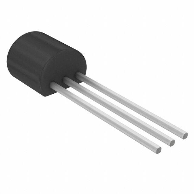
TO-92
Bag
TO-92
Tape and reel
Ammopack
The LM217L/LM317L are monolithic integrated
circuits in SO-8 and TO-92 packages intended for
use as positive adjustable voltage regulators.
They are designed to supply up to 100 mA of load
current with an output voltage adjustable over a
1.2 to 37 V range.The nominal output voltage is
selected by means of only a resistive divider,
making the device exceptionally easy to use and
eliminating the stocking of many fixed regulators.
SO-8
Features
• Outuput voltage range: 1.2 to 37 V
• Output current up to 100 mA
• Line regulation typ. 0.01%
• Load regulation typ. 0.1%
• Thermal overload protection
• Short-circuit protection
• Output transition safe area compensation
• Floating operation for high voltage applications
Table 1. Device summary
Order codes
SO-8 (tape and reel)
TO-92 (Bag)
TO-92 (Ammopack)
LM217LD13TR
LM317LD13TR
TO-92 (tape and reel)
LM217LZ-TR
LM317LZ
September 2015
This is information on a product in full production.
LM317LZ-AP
DocID2168 Rev 7
LM317LZ-TR
1/23
www.st.com
�Contents
LM217L, LM317L
Contents
1
Diagram . . . . . . . . . . . . . . . . . . . . . . . . . . . . . . . . . . . . . . . . . . . . . . . . . . . 3
2
Pin configuration . . . . . . . . . . . . . . . . . . . . . . . . . . . . . . . . . . . . . . . . . . . 4
3
Maximum ratings . . . . . . . . . . . . . . . . . . . . . . . . . . . . . . . . . . . . . . . . . . . . 5
4
Electrical characteristics . . . . . . . . . . . . . . . . . . . . . . . . . . . . . . . . . . . . . 6
5
Typical performance . . . . . . . . . . . . . . . . . . . . . . . . . . . . . . . . . . . . . . . . . 8
6
Application information . . . . . . . . . . . . . . . . . . . . . . . . . . . . . . . . . . . . . . 9
7
Application circuits . . . . . . . . . . . . . . . . . . . . . . . . . . . . . . . . . . . . . . . . . 10
8
Package information . . . . . . . . . . . . . . . . . . . . . . . . . . . . . . . . . . . . . . . . 12
9
2/23
8.1
TO-92 Bag package information . . . . . . . . . . . . . . . . . . . . . . . . . . . . . . . 12
8.2
TO-92 Ammopack package information . . . . . . . . . . . . . . . . . . . . . . . . . . 13
8.3
TO-92 packing information . . . . . . . . . . . . . . . . . . . . . . . . . . . . . . . . . . . . 15
8.4
SO-8 package information . . . . . . . . . . . . . . . . . . . . . . . . . . . . . . . . . . . . 17
8.5
SO-8 packing information . . . . . . . . . . . . . . . . . . . . . . . . . . . . . . . . . . . . . 20
Revision history . . . . . . . . . . . . . . . . . . . . . . . . . . . . . . . . . . . . . . . . . . . 22
DocID2168 Rev 7
�LM217L, LM317L
1
Diagram
Diagram
Figure 1. Schematic diagram
DocID2168 Rev 7
3/23
23
�Pin configuration
2
LM217L, LM317L
Pin configuration
Figure 2. Pin connections (top view for SO-8, bottom view for TO-92)
PIN 1 = ADJUST
PIN 2 = IN
PIN 3 = OUT
SO-8
4/23
TO-92
DocID2168 Rev 7
�LM217L, LM317L
3
Maximum ratings
Maximum ratings
Table 2. Absolute maximum ratings
Symbol
VI-VO
Parameter
Input-output differential voltage
PD
Power dissipation
TOP
Operating junction temperature range
TSTG
Storage temperature range
Value
Unit
40
V
Internally limited
mW
for LM217L
-40 to 125
for LM317L
0 to 125
°C
-55 to 150
°C
Table 3. Thermal data
Symbol
Parameter
SO-8
RthJC
Thermal resistance junction-case (max)
20
RthJA
Thermal resistance junction-ambient (max)
55(1)(2)
TO-92
Unit
°C/W
200
1. Considering 6 cm² of copper Board heat-sink.
2. Our SO-8 package used for voltage regulators is modified internally to have pins 2, 3, 6 and 7 electrically communed to the
die attach flag. This particular frame decreases the total thermal resistance of the package and increases its ability to
dissipate power when an appropriate area of copper on the printed circuit board is available for heat-sinking. The external
dimensions are the same as for the standard SO-8.
Figure 3. Test circuit
,Q
2XW
$GM
*,3*�����������59
DocID2168 Rev 7
5/23
23
�Electrical characteristics
4
LM217L, LM317L
Electrical characteristics
(Refer to the test circuits, TJ = - 40 to 125°C, VI - VO = 5 V, IO = 40 mA, unless otherwise
specified)
Table 4. Electrical characteristics of LM217L
Symbol
∆VO
Parameter
Line regulation
Test conditions
VI - VO = 3 to 40 V, IO = 20 mA
VO ≤ 5 V, IO = 5 to 100 mA
∆VO
Min.
TJ = 25°C
∆IADJ
Adjustment pin current
VI - VO = 3 to 40 V, IO = 5 to 100 mA
Pd < 625 mW
VREF
Reference voltage
VI - VO = 3 to 40 V, IO = 10 to 100 mA
Pd < 625 mW
0.02
0.02
0.05
5
15
20
50
0.1
0.3
0.3
1
50
100
µA
0.2
5
µA
1.25
1.3
V
%
1.2
Output voltage temperature
stability
IO(min)
Minimum load current
IO(max)
Maximum output current
0.7
VI - VO = 40 V
3.5
VI - VO = 3 to 13 V
100
5
mA
200
50
Output noise voltage
B = 10 Hz to 10 KHz, TJ = 25°C
Supply voltage rejection (1)
TJ = 25°C
f = 120 Hz
DocID2168 Rev 7
%
mA
VI - VO = 40 V
1. CADJ is connected between adjust pin and ground.
6/23
0.01
mV
TJ = 25°C
Adjustment pin current
SVR
Unit
%/V
TJ = 25°C
IADJ
eN
Max.
Load regulation
VO ≥ 5 V, IO = 5 to 100 mA
∆VO/VO
Typ.
0.003
CADJ = 0
CADJ = 10 µF
%
65
dB
66
80
�LM217L, LM317L
Electrical characteristics
(Refer to the test circuits, TJ = 0 to 125°C, VI - VO = 5 V, IO = 40 mA, unless otherwise
specified)
Table 5. Electrical characteristics of LM317L
Symbol
∆VO
Parameter
Line regulation
Test conditions
VI - VO = 3 to 40 V, IO = 20 mA
VO ≤ 5 V, IO = 5 to 100 mA
∆VO
Min.
TJ = 25°C
0.01
0.04
0.02
0.07
5
25
20
70
0.1
0.5
0.3
1.5
50
100
µA
0.2
5
µA
1.25
1.3
V
mV
TJ = 25°C
Adjustment pin current
∆IADJ
Adjustment pin current
VI - VO = 3 to 40 V, IO = 5 to 100 mA
Pd < 625 mW
VREF
Reference voltage
VI - VO = 3 to 40 V, IO = 5 to 100 mA
Pd < 625 mW
%
1.2
Output voltage
temperature stability
IO(min)
Minimum load current
IO(max)
Maximum output current
SVR
Unit
%/V
TJ = 25°C
IADJ
eN
Max.
Load regulation
VO ≥ 5 V, IO = 5 to 100 mA
∆VO/VO
Typ.
0.7
VI - VO = 40 V
3.5
VI - VO = 3 to 13 V
100
%
5
mA
200
mA
VI - VO = 40 V
50
Output noise voltage
B = 10 Hz to 10 KHz, TJ = 25°C
Supply voltage rejection (1)
TJ = 25°C
f = 120 Hz
0.003
CADJ = 0
CADJ = 10 µF
%
65
dB
66
80
1. CADJ is connected between adjust pin and ground.
DocID2168 Rev 7
7/23
23
�Typical performance
5
LM217L, LM317L
Typical performance
Figure 4. Current limit
,R
�P$�
Figure 5. Minimum operating current
,R
�P$�
7-� ����&
���
7-� ����&
���
���
���
���
���
���
���
���
�
8/23
��
��
�� 9LQ �9R���9�
DocID2168 Rev 7
�
��
��
�� 9LQ �9R���9�
�LM217L, LM317L
6
Application information
Application information
The LM317L provides an internal reference voltage of 1.25 V between the output and
adjustments terminals. This is used to set a constant current flow across an external resistor
divider (see Figure 6.), giving an output voltage VO of:
VO = VREF (1 + R2/R1) + IADJ R2
The device was designed to minimize the term IADJ (100 µA max) and to maintain it very
constant with line and load changes. Usually, the error term IADJ × R2 can be neglected. To
obtain the previous requirement, all the regulator quiescent current is returned to the output
terminal, imposing a minimum load current condition. If the load is insufficient, the output
voltage will rise.
Since the LM317L is a floating regulator and "sees" only the input-to-output differential
voltage, supplies of very high voltage with respect to ground can be regulated as regulator
as the maximum input-to-output differential is not exceeded. Furthermore, programmable
regulators are easily obtainable and, by connecting a fixed resistor between the adjustment
and output, the device can be used as a precision current regulator. In order to optimize the
load regulation, the current set resistor R1 (see Figure 6.) should be tied as close as
possible to the regulator, while the ground terminal of R2 should be near the ground of the
load to provide remote ground sensing.
DocID2168 Rev 7
9/23
23
�Application circuits
7
LM217L, LM317L
Application circuits
Figure 6. Basic adjustable regulator
"EK
*,3*�����������59
Figure 7. Voltage regulator with protection diodes
"EK
*,3*�����������59
Figure 8. Slow turn-on 15 V regulator
$GM
*,3*�����������59
10/23
DocID2168 Rev 7
�LM217L, LM317L
Application circuits
Figure 9. Current regulator
,2 95()�5����,$'- �����9�5�
*,3*�����������59
Figure 10. 5 V Electronic shut-down regulator
$GM
*,3*�����������59
Figure 11. Digitally selected outputs
$GM
�5�� �VHWV�PD[LPXP�92�
DocID2168 Rev 7
*,3*�������������59
11/23
23
�Package information
8
LM217L, LM317L
Package information
In order to meet environmental requirements, ST offers these devices in different grades of
ECOPACK® packages, depending on their level of environmental compliance. ECOPACK®
specifications, grade definitions and product status are available at: www.st.com.
ECOPACK® is an ST trademark.
8.1
TO-92 Bag package information
Figure 12. TO-92 Bag package outline
0102782 D
12/23
DocID2168 Rev 7
�LM217L, LM317L
Package information
Table 6. TO-92 Bag mechanical data
mm
Dim.
Min.
Typ.
A
4.32
4.95
b
0.36
0.51
D
4.45
4.95
E
3.30
3.94
e
2.41
2.67
e1
1.14
1.40
L
12.70
15.49
R
2.16
2.41
S1
0.92
1.52
W
0.41
0.56
V
8.2
Max.
5°
TO-92 Ammopack package information
Figure 13. TO-92 Ammopack package outline
T
T
A1
A1
H1
H1
H
H
T2
T2
T1
T1
delta
delta H
H
H3
H3
H0
H0
L
L
d
d
W2
W2
l1
l1
W
W0
W
W0
W1
W1
F1
F1 F2
F2
F3
F3
P2
P2
P0
P0
D0
D0
tt
0050910S_Rev_U
0050910S_Rev_U
DocID2168 Rev 7
13/23
23
�Package information
LM217L, LM317L
Table 7. TO-92 Ammopack mechanical data
mm
Dim.
Min.
Typ.
A1
4.80
T
3.80
T1
1.60
T2
2.30
d
0.45
0.47
0.48
P0
12.50
12.70
12.90
P2
5.65
6.35
7.05
F1, F2
2.40
2.50
2.94
F3
4.98
5.08
5.48
delta H
-2.00
W
17.50
18.00
19.00
W0
5.5
6.00
6.5
W1
8.50
9.00
9.25
2.00
W2
0.50
H
18.50
21
H3
0.5
1
2
H0
15.50
16.00
18.8
25.0
27.0
4.00
4.20
H1
D0
14/23
Max.
3.80
t
0.90
L
11.00
l1
3.00
delta P
-1.00
DocID2168 Rev 7
1.00
�LM217L, LM317L
8.3
Package information
TO-92 packing information
Figure 14. TO-92 tape and reel outline
delta P
T
A1
T2
H1
T1
delta H
H
H0
d
L
W2
l1
W
W0
W1
F1 F2
P2
D0
t
P0
DocID2168 Rev 7
15/23
23
�Package information
LM217L, LM317L
Table 8. TO-92 tape and reel mechanical data
mm
Dim.
Min.
Typ.
A1
4.80
T
3.80
T1
1.60
T2
2.30
d
0.45
0.47
0.48
P0
12.50
12.70
12.90
P2
5.65
6.35
7.05
F1, F2
2.40
2.50
2.94
F3
4.98
5.08
5.48
delta H
-2.00
W
17.50
18.00
19.00
W0
5.5
6.00
6.5
W1
8.50
9.00
9.25
2.00
W2
0.50
H
18.50
21
H3
0.5
1
2
H0
15.50
16.00
18.8
25.0
27.0
4.00
4.20
H1
D0
16/23
Max.
3.80
t
0.90
L
11.00
l1
3.00
delta P
-1.00
Ø1
352
355
358
Ø2
28
30
32
u
44
47
50
DocID2168 Rev 7
1.00
�LM217L, LM317L
8.4
Package information
SO-8 package information
Figure 15. SO-8 package outline
0016023_G_FU
DocID2168 Rev 7
17/23
23
�Package information
LM217L, LM317L
Table 9. SO-8 mechanical data
mm
Dim.
Min.
Typ.
A
1.75
A1
0.10
0.25
A2
1.25
b
0.31
0.51
b1
0.28
0.48
c
0.10
0.25
c1
0.10
0.23
D
4.80
4.90
5.00
E
5.80
6.00
6.20
E1
3.80
3.90
4.00
e
1.27
h
0.25
0.50
L
0.40
1.27
L1
1.04
L2
0.25
k
0°
8°
ccc
18/23
Max.
0.10
DocID2168 Rev 7
�LM217L, LM317L
Package information
Figure 16. SO-8 recommended footprint
Footprint_0016023_G_FU
DocID2168 Rev 7
19/23
23
�Package information
8.5
LM217L, LM317L
SO-8 packing information
Figure 17. SO-8 tape and reel outline
20/23
DocID2168 Rev 7
�LM217L, LM317L
Package information
Table 10. SO-8 tape and reel mechanical data
mm
Dim.
Min.
Typ.
A
Max.
330
C
12.8
D
20.2
N
60
13.2
T
22.4
Ao
8.1
8.5
Bo
5.5
5.9
Ko
2.1
2.3
Po
3.9
4.1
P
7.9
8.1
DocID2168 Rev 7
21/23
23
�Revision history
9
LM217L, LM317L
Revision history
Table 11. Revision history
Date
Revision
16-Mar-2005
2
Add Tape & reel for TO-92.
23-Dec-2005
3
Mistake on ordering table in header.
18-May-2007
4
Order codes has been updated and the document has been reformatted.
5
Added TO-92 Ammopack package.
Updated Section 6: Application information and Section 8: Package
information.
Added Section 8.5: SO-8 packing information.
Minor text changes.
19-May-2015
6
Updated the features in cover page, Table 4: Electrical characteristics of
LM217L, Table 5: Electrical characteristics of LM317L and Figure 4: Current
limit.
Added Table 3: Thermal data.
Minor text changes.
17-Sep-2015
7
Updated Table 1: Device summary.
Minor text changes.
20-May-2014
22/23
Changes
DocID2168 Rev 7
�LM217L, LM317L
IMPORTANT NOTICE – PLEASE READ CAREFULLY
STMicroelectronics NV and its subsidiaries (“ST”) reserve the right to make changes, corrections, enhancements, modifications, and
improvements to ST products and/or to this document at any time without notice. Purchasers should obtain the latest relevant information on
ST products before placing orders. ST products are sold pursuant to ST’s terms and conditions of sale in place at the time of order
acknowledgement.
Purchasers are solely responsible for the choice, selection, and use of ST products and ST assumes no liability for application assistance or
the design of Purchasers’ products.
No license, express or implied, to any intellectual property right is granted by ST herein.
Resale of ST products with provisions different from the information set forth herein shall void any warranty granted by ST for such product.
ST and the ST logo are trademarks of ST. All other product or service names are the property of their respective owners.
Information in this document supersedes and replaces information previously supplied in any prior versions of this document.
© 2015 STMicroelectronics – All rights reserved
DocID2168 Rev 7
23/23
23
�


 工商网监
湘ICP备2023018690号
工商网监
湘ICP备2023018690号
