LPS27HHTW
Datasheet
MEMS pressure sensor: 260-1260 hPa absolute digital output barometer with
embedded temperature sensor in water-resistant package
Features
•
•
•
•
•
•
•
•
•
•
Pressure sensor with water-resistant package
Potting gel and grounded metal cap
260 to 1260 hPa absolute pressure range
Current consumption down to 4 µA
Absolute pressure accuracy: 0.5 hPa
Low pressure sensor noise: 0.7 Pa
Temperature accuracy: ±1.5 °C
Embedded temperature compensation
24-bit pressure data output
ODR from 1 Hz to 200 Hz
•
•
•
•
•
SPI, I²C or MIPI I3CSM interfaces
Embedded FIFO
Interrupt functions: Data-Ready, FIFO flags, pressure thresholds
Supply voltage: 1.7 to 3.6 V
ECOPACK lead-free compliant
Applications
Product status link
LPS27HHTW
Product summary
Order code
LPS27HHTWTR
Temp. range [°C]
-40 to +85°C
Package
CCLGA-10L
Packing
Tape and reel
Product label
•
•
•
•
•
•
•
Altimeters and barometers for portable devices
GPS applications
Weather station equipment
Sport watches
e-cigarettes
Water depth monitoring
Gas metering
Description
The LPS27HHTW is an ultra-compact piezoresistive absolute pressure sensor which
functions as a digital output barometer. The device also embeds a temperature
sensor to monitor ambient temperature. The LPS27HHTW comprises a sensing
element and an IC interface which communicates through I²C, MIPI I3CSM or SPI
from the sensing element to the application.
The sensing element, which detects absolute pressure, consists of a suspended
membrane manufactured using a dedicated process developed by ST.
The LPS27HHTW is available in a ceramic LGA package with metal lid. It is
guaranteed to operate over a temperature range extending from -40 °C to +85 °C.
The package is holed to allow external pressure to reach the sensing element. Gel
inside the IC protects the electrical components from water and the metal cap is
grounded electrically for better ESD robustness.
DS13489 - Rev 1 - January 2021
For further information contact your local STMicroelectronics sales office.
www.st.com
�LPS27HHTW
Block diagrams
1
Block diagrams
Figure 1. Device architecture block diagram
Temperature
Sensor
I2C
Analog
Front-End
MUX
Digital
Logic
ADC
MIPI I3CSM
SPI
Sensing Element
Sensor Bias
Voltage and Current Bias
Clock and timing
Figure 2. Digital logic
Digital
LP Filter
LPF1
Digital
LP Filter
Analog
Front-End
LPF0
1
Pout
Pressure
Compensation
0
ADC
Temperature
Compensation
DS13489 - Rev 1
EN_LPFP
Output
Registers
I2C
MIPI I3CSM
Tout
FIFO
SPI
page 2/55
�LPS27HHTW
Pin description
2
Pin description
GND
9
GND
8
SCL/SPC
2
GND
7
6
CS
10
1
INT_DRDY
VDD
Vdd_IO
Figure 3. Pin connections (bottom view)
3
RES
4
SDA/SDI/SDO
5
SDO/SA0
Table 1. Pin description
Pin number
Name
1
Vdd_IO
2
3
4
Power supply for I/O pins
SCL
I²C / MIPI I3CSM serial clock (SCL)
SPC
SPI serial port clock (SPC)
Reserved
Connect to GND
SDA
I²C / MIPI I3CSM serial data (SDA)
SDI
4-wire SPI serial data input (SDI)
SDI/SDO
5
Function
SDO
SA0
3-wire serial data input/output (SDI/SDO)
4-wire SPI serial data output (SDO)
I²C least significant bit of the device address (SA0)
MIPI I3CSM least significant bit of the static address (SA0)
SPI enable
6
CS
I²C and MIPI I3CSM / SPI mode selection
(1: SPI idle mode / I²C and MIPI I3CSM communication enabled;
0: SPI communication mode / I²C and MIPI I3CSM disabled)
DS13489 - Rev 1
7
INT_DRDY
Interrupt or Data-Ready
8
GND
0 V supply
9
GND
0 V supply
10
VDD
Power supply
page 3/55
�LPS27HHTW
Mechanical and electrical specifications
3
Mechanical and electrical specifications
3.1
Mechanical characteristics
VDD = 1.8 V, T = 25 °C, unless otherwise noted.
Table 2. Pressure and temperature sensor characteristics
Symbol
Parameter
Test condition
Min.
Typ.(1)
Max.
Unit
Pressure sensor characteristics
PTop
Operating temperature range
-40
+85
°C
Pop
Operating pressure range
260
1260
hPa
Pbits
Pressure output data
Psens
Pressure sensitivity
PAccRel
Relative accuracy over pressure (2)
PAccT
Absolute accuracy over temperature
Pnoise
RMS pressure sensing noise(3)
P= 800 - 1100 hPa, T = 25 °C
24
bits
4096
LSB/hPa
±0.025
hPa
P = 860 ~ 1160 hPa, T = 25 ~ 65°C
±0.5
P = 260 ~ 1260 hPa, T = 0 ~ 65 °C
±1
with embedded filter and at T = 25 °C
hPa
0.007
hPa RMS
1
10
25
ODRPres
Pressure output data rate
(4)
50
Hz
75
100
200
TCO
Temperature coefficient offset
P_longterm
Pressure accuracy, long-term stability
P_drift
Soldering drift
P = 860 ~ 1160 hPa, T = -20 ~ +65 °C
0.75
Pa/°C
1
hPa/year
±0.5
hPa
Temperature sensor characteristics
Top
Operating temperature range
Tacc
Temperature absolute accuracy
Tsens
Temperature sensitivity
-40
25 ~ 65 °C
+85
°C
±1.5
°C
100
LSB/°C
1
10
25
ODRT
Temperature output data rate
50
Hz
75
100
200
1. Typical specifications are not guaranteed.
2. By design, the typ. value is defined based characterization data with 10 hPa pressure interval.
3. Pressure noise RMS evaluated in a controlled environment, based on the average standard deviation of 50
measurements with LOW_NOISE_EN = 1, EN_LPFP = 1, LPFP_CFG = 1.
4. Output data rate is configured acting on ODR[2:0] in CTRL_REG1 (10h).
DS13489 - Rev 1
page 4/55
�LPS27HHTW
Electrical characteristics
3.2
Electrical characteristics
VDD = 1.8 V, T = 25 °C, unless otherwise noted.
Table 3. Electrical characteristics
Symbol
VDD
Vdd_IO
Parameter
Test condition
Min.
Unit
1.7
3.6
V
IO supply voltage
1.7
Vdd+0.1
V
4
LOW_NOISE_EN = 0
Supply current
µA
@ ODR 1 Hz
12
LOW_NOISE_EN = 1
IddPdn
Max.
Supply voltage
@ ODR 1 Hz
Idd
Typ.(1)
Supply current in power-down mode
0.9
µA
1. Typical specifications are not guaranteed.
Table 4. DC characteristics
Symbol
Parameter
Condition
Min.
Typ.
Max.
Unit
0.3 * Vdd
V
DC input characteristics
Vil
Low-level input voltage (Schmitt buffer)
Vih
High-level input voltage (Schmitt buffer)
0.7 * Vdd
V
DC output characteristics
DS13489 - Rev 1
Vol
Low-level output voltage
Voh
High-level output voltage
0.2
Vdd - 0.2
V
V
page 5/55
�LPS27HHTW
Communication interface characteristics
3.3
Communication interface characteristics
3.3.1
SPI - serial peripheral interface
Subject to general operating conditions for Vdd and TOP.
Table 5. SPI slave timing values
Symbol
Parameter
Value(1)
Min.
tc(SPC)
SPI clock cycle
fc(SPC)
SPI clock frequency
tsu(CS)
CS setup time
6
th(CS)
CS hold time
8
tsu(SI)
SDI input setup time
5
th(SI)
SDI input hold time
15
tv(SO)
SDO valid output time
th(SO)
SDO output hold time
tdis(SO)
SDO output disable time
Max.
Unit
ns
100
10(2)
MHz
ns
50
9
50
1. Values are guaranteed at 10 MHz clock frequency for SPI with both 4 and 3 wires, based on characterization results, not
tested in production.
2. Recommended to set max SPI clock 8 MHz to ≤50 Hz ODR.
Figure 4. SPI slave timing diagram
Note: Measurement points are done at 0.3·Vdd_IO and 0.7·Vdd_IO for both ports.
DS13489 - Rev 1
page 6/55
�LPS27HHTW
Communication interface characteristics
3.3.2
I²C - inter-IC control interface
Subject to general operating conditions for Vdd and TOP.
Table 6. I²C slave timing values
Symbol
f(SCL)
I²C standard mode(1)
Parameter
I²C fast mode(1)
Min.
Max
Min.
Max.
0
100
0
400
SCL clock frequency
tw(SCLL)
SCL clock low time
4.7
1.3
tw(SCLH)
SCL clock high time
4.0
0.6
tsu(SDA)
SDA setup time
250
100
th(SDA)
SDA data hold time
0
th(ST)
START condition hold time
4
0.6
tsu(SR)
Repeated START condition setup time
4.7
0.6
tsu(SP)
STOP condition setup time
4
0.6
4.7
1.3
tw(SP:SR)
Bus free time between STOP and START condition
3.45
Unit
kHz
µs
ns
0
0.9
µs
µs
1. Data based on standard I²C protocol requirement, not tested in production.
Figure 5. I²C slave timing diagram
REPEATED
START
START
tsu(SR)
tw(SP:SR)
SDA
tsu(SDA)
START
th(SDA)
tsu(SP)
STOP
SCL
th(ST)
tw(SCLL)
tw(SCLH)
Note: Measurement points are done at 0.3·Vdd_IO and 0.7·Vdd_IO for both ports.
DS13489 - Rev 1
page 7/55
�LPS27HHTW
Absolute maximum ratings
3.4
Absolute maximum ratings
Stress above those listed as “Absolute maximum ratings” may cause permanent damage to the device. This is
a stress rating only and functional operation of the device under these conditions is not implied. Exposure to
maximum rating conditions for extended periods may affect device reliability.
Table 7. Absolute maximum ratings
Symbol
Vdd
Vdd_IO
Vin
P(water)
Ratings
Maximum value
Unit
Supply voltage
-0.3 to 4.8
V
I/O pins supply voltage
-0.3 to 4.8
V
-0.3 to Vdd_IO +0.3
V
1
MPa
-40 to +125
°C
2 (HBM)
kV
Input voltage on any control pin
Overpressure
TSTG
Storage temperature range
ESD
Electrostatic discharge protection
Note: Supply voltage on any pin should never exceed 4.8 V.
This device is sensitive to mechanical shock, improper handling can cause permanent damage to the part.
This device is sensitive to electrostatic discharge (ESD), improper handling can cause permanent damage to the part.
DS13489 - Rev 1
page 8/55
�LPS27HHTW
Functionality
4
Functionality
The LPS27HHTW is a high-resolution, digital output pressure sensor packaged in a CCLGA package with metal
lid. The complete device includes a sensing element based on a piezoresistive Wheatstone bridge approach, and
an IC interface which communicates a digital signal from the sensing element to the application.
4.1
Sensing element
An ST proprietary process is used to obtain a silicon membrane for MEMS pressure sensors. When pressure is
applied, the membrane deflection induces an imbalance in the Wheatstone bridge piezoresistances whose output
signal is converted by the IC interface.
4.2
IC interface
The complete measurement chain is composed of a low-noise amplifier which converts the resistance unbalance
of the MEMS sensors (pressure and temperature) into an analog voltage using an analog-to-digital converter.
The pressure and temperature data may be accessed through an I²C/MIPI I3CSM/SPI interface thus making the
device particularly suitable for direct interfacing with a microcontroller.
The LPS27HHTW features a Data-Ready signal which indicates when a new set of measured pressure and
temperature data are available, thus simplifying data synchronization in the digital system that uses the device.
4.3
Factory calibration
The trimming values are stored inside the device in a non-volatile structure. When the device is turned on, the
trimming parameters are downloaded into the registers to be employed during the normal operation which allows
the device to be used without requiring any further calibration.
DS13489 - Rev 1
page 9/55
�LPS27HHTW
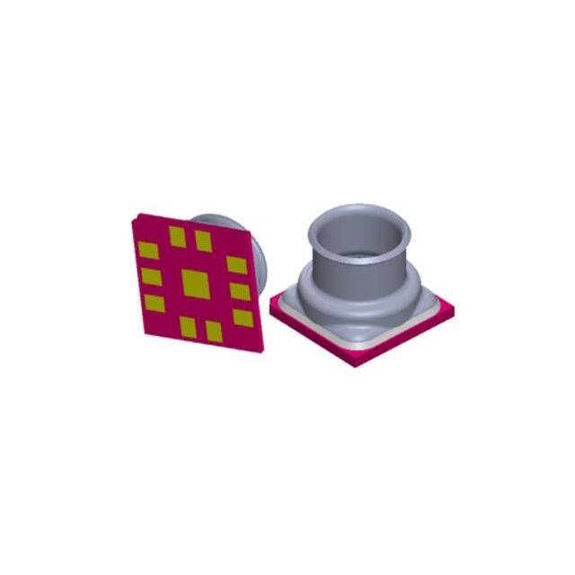
Device structure
4.4
Device structure
The LPS27HHTW has a unique cylindrical package solution with a full metal lid assembled on ceramic substrate
and this cylindrical package provides an easy assembly with O-rings in the end user’s application.
Figure 6. LPS27HHTW internal structure
This structure (Figure 6) is designed and verified to resist water pressure up to 10 ATM and the potting gel in the
LPS27HHTW has been proven to protect electronic components from long-term exposure to harsh environments
such as water mixed with chlorine, bromine, commercial washing detergent and fuels, solvents and chemicals.
It also provides excellent low-stress encapsulation performance for sensitive electronic components from severe
environmental conditions such as high temperature and humidity, refer to the properties of the gel which are given
in the following table.
Table 8. Potting gel properties
Properties
Permeability g/m²·24 hr
7
Hardness (penetration) based on ASTM D1403
70
Ultra-low Young's modulus
TCE (Thermal Coefficient of Expansion)
DS13489 - Rev 1
Potting gel
Less than 0.01 GPa
300 ppm/°C
page 10/55
�LPS27HHTW
Interpreting pressure readings
4.5
Interpreting pressure readings
The pressure data are stored in 3 registers: PRESS_OUT_H (2Ah), PRESS_OUT_L (29h), and PRESS_OUT_XL
(28h). The value is expressed as a 24-bit signed number (in 2’s complement).
To obtain the pressure in hPa, take the complete 24-bit word and then divide by the sensitivity 4096 LSB/
hPa. This same interpretation is applied to pressure readings when FIFO is enabled and the pressure
data are stored in 3 registers: FIFO_DATA_OUT_PRESS_XL (78h), FIFO_DATA_OUT_PRESS_L (79h), and
FIFO_DATA_OUT_PRESS_H (7Ah).
Figure 7. Pressure readings
Pressure Value LSB = PRESS_OUT_H 2Aℎ & PRESS_OUT_L 29ℎ & PRESS_OUT_XL
28ℎ = 3FF58Dℎ = 4191629 LSB signed decimal
Pressure ℎPa =
4.6
(1)
Pressure Value LSB
= 4191629 LSB = 1023 ℎPa
Sensitivity
4096 LSB/ℎPA
(2)
Interpreting temperature readings
The temperature data are stored in 2 registers: TEMP_OUT_H (2Ch) and TEMP_OUT_L (2Bh).
The value is expressed as 2’s complement. To obtain the temperature in °C, take the two’s complement
of the complete 16-bit word and then divide by the sensitivity 100 LSB/°C. This same interpretation is
applied to temperature readings when FIFO is enabled and the temperature data are stored in 2 registers:
FIFO_DATA_OUT_TEMP_H (7Ch) and FIFO_DATA_OUT_TEMP_L (7Bh).
Figure 8. Temperature readings
TEMP_OUT_H
0 0 0 0 1 0 0 1
TEMP_OUT_L
1 1 0 0 0 1 0 0
Temperature Value (LSB) = TEMP_OUT_H (2Ch) & TEMP_OUT_L (2Bh)
= 09C4 = 2500 LSB (decimal signed)
Temperature (°C) =
DS13489 - Rev 1
Temperature Value (LSB)
2500 LSB
=
= 25.00°C
Sensitivity
100 LSB/°C
page 11/55
�LPS27HHTW
FIFO
5
FIFO
The LPS27HHTW embeds 128 slots of 40-bit data FIFO to store the pressure and temperature output values.
This allows consistent power saving for the system, since the host processor does not need to continuously poll
data from the sensor, but it can wake up only when needed and burst the significant data out from the FIFO. This
buffer can work according to six different modes:
•
Bypass mode
•
FIFO mode
•
Continuous (Dynamic-Stream) mode
•
Continuous (Dynamic-Stream)-to-FIFO mode
•
Bypass-to-Continuous (Dynamic-Stream)
•
Bypass-to-FIFO mode
The FIFO buffer is enabled when a configuration different from all bits '0' are written in FIFO_CTRL (13h) and
each mode is selected by the TRIG_MODES bit and F_MODE[1:0] bits in FIFO_CTRL (13h). Programmable
FIFO threshold status, FIFO overrun events and the number of unread samples stored are available in the
FIFO_STATUS1 (25h) and FIFO_STATUS2 (26h) registers and can be set to generate dedicated interrupts on the
INT_DRDY pad using the CTRL_REG3 (12h) register.
FIFO_STATUS2 (26h)(FIFO_WTM_IA) goes to '1' when the number of unread samples (FIFO_STATUS1 (25h)
(FSS[7:0]) is greater than or equal to WTM[6:0] in FIFO_WTM (14h). If FIFO_WTM (14h)(WTM[6:0]) is equal to 0,
FIFO_STATUS2 (26h)(FIFO_WTM_IA) stays at '0'.
FIFO_STATUS2 (26h)(FIFO_OVR_IA) is equal to '1' if a FIFO slot is overwritten.
FIFO_STATUS1 (25h)(FSS[7:0]) contains stored data levels of unread samples; when FSS[7:0] is equal to
‘00000000’, FIFO is empty; when FSS[7:0] is equal to ‘10000000’, FIFO is full and the unread samples are 128.
DS13489 - Rev 1
page 12/55
�LPS27HHTW
Bypass mode
5.1
Bypass mode
In Bypass mode (FIFO_CTRL (13h)(TRIG_MODES and F_MODE[1:0] = ‘000’ or ‘100’), the FIFO is not
operational and it remains empty.
Switching to Bypass mode is also used to reset the FIFO. Passing through Bypass mode is mandatory when
switching between different FIFO buffer operating modes.
As described in the next figure, for each channel only the first address is used. When new data is available, the
older data is overwritten.
Figure 9. Bypass mode
P i ,T i
empty
DS13489 - Rev 1
P0
T0
P1
T1
P2
T2
P127
T127
page 13/55
�LPS27HHTW
FIFO mode
5.2
FIFO mode
In FIFO mode (FIFO_CTRL (13h)(TRIG_MODES and F_MODE[1:0] = ‘001’) data from the output
PRESS_OUT_XL (28h), PRESS_OUT_L (29h), PRESS_OUT_H (2Ah), TEMP_OUT_L (2Bh), and
TEMP_OUT_H (2Ch) are stored in the FIFO until it is full.
To reset FIFO content, in order to select Bypass mode the value '000' must be written in FIFO_CTRL (13h)
(TRIG_MODE & F_MODE[1:0]). After this reset command it is possible to restart FIFO mode by writing the value
'001' in FIFO_CTRL (13h)(TRIG_MODE & F_MODE[1:0]).
The FIFO buffer memorizes 128 levels of data, but the depth of the FIFO can be resized/reduced by setting
the FIFO_CTRL (13h)(STOP_ON_WTM) bit. If the STOP_ON_WTM bit is set to '1', FIFO depth is limited to
FIFO_WTM (14h)(WTM[6:0]) data.
Figure 10. FIFO mode
P i ,T i
DS13489 - Rev 1
P0
T0
P1
T1
P2
T2
P127
T127
page 14/55
�LPS27HHTW
Continuous (Dynamic-Stream) mode
5.3
Continuous (Dynamic-Stream) mode
In Continuous (Dynamic-Stream) mode (FIFO_CTRL (13h)(TRIG_MODES and F_MODE[1:0] = ‘011’) after
emptying the FIFO, the first new sample that arrives becomes the first to be read in a subsequent read burst. In
this way, the number of new data available in FIFO does not depend on the previous read.
In Continuous (Dynamic-Stream) mode FIFO_STATUS1 (25h)(FSS[7:0]) is the number of new pressure and
temperature samples available in the FIFO buffer.
Continuous (Dynamic-Stream) is intended to be used to read FIFO_STATUS1 (25h)(FSS[7:0]) samples when it is
not possible to guarantee reading data within 1/ODR time period.
Also, a FIFO threshold interrupt on the INT_DRDY pad through CTRL_REG3 (12h)(INT_F_WTM) can be enabled
in order to read data from the FIFO and leave free memory slots for incoming data.
Figure 11. Continuous (Dynamic-Stream) mode
DS13489 - Rev 1
page 15/55
�LPS27HHTW
Bypass-to-FIFO mode
5.4
Bypass-to-FIFO mode
In Bypass-to-FIFO mode (FIFO_CTRL (13h)(TRIG_MODES and F_MODE[1:0] = ‘101’), FIFO behavior switches
when the INT_SOURCE (24h)(IA) bit rises for the first time. When the INT_SOURCE (24h)(IA) bit is equal to '0',
FIFO behaves like in Bypass mode. Once the INT_SOURCE (24h)(IA) bit rises to '1', FIFO behavior switches and
keeps behaving like in FIFO mode.
An interrupt generator has to be set to the desired configuration through INTERRUPT_CFG (0Bh).
Figure 12. Bypass-to-FIFO mode
P i ,T i
empty
P i ,T i
P0
T0
T1
P1
T1
P2
T2
P2
T2
P127
T127
P127
T127
P0
T0
P1
Bypass Mode
FIFO Mode
Trigger event
DS13489 - Rev 1
page 16/55
�LPS27HHTW
Bypass-to-Continuous (Dynamic-Stream) mode
5.5
Bypass-to-Continuous (Dynamic-Stream) mode
In Bypass-to-Continuous (Dynamic-Stream) mode (FIFO_CTRL (13h)(TRIG_MODES and F_MODE[1:0] = ‘110’),
FIFO operates in Bypass mode until it switches to Continuous (Dynamic-Stream) mode behavior when
INT_SOURCE (24h)(IA) rises to '1', then FIFO behavior keeps behaving like in Continuous (Dynamic-Stream)
mode.
An interrupt generator has to be set to the desired configuration through INTERRUPT_CFG (0Bh).
Figure 13. Bypass-to-Continuous (Dynamic-Stream) mode
P i ,T i
empty
T0
T1
P1
T1
T2
P2
T2
P126
T126
P127
T127
T0
P1
P2
P127
P i ,T i
P0
P0
T127
Bypass Mode
Dynamic-Stream Mode
Trigger event
DS13489 - Rev 1
page 17/55
�LPS27HHTW
Continuous (Dynamic-Stream)-to-FIFO mode
5.6
Continuous (Dynamic-Stream)-to-FIFO mode
In Continuous (Dynamic-Stream)-to-FIFO mode (FIFO_CTRL (13h)(TRIG_MODES and F_MODE[1:0] = ‘111’),
data are stored in FIFO and FIFO operates in Continuous (Dynamic-Stream) mode behavior until it switches to
FIFO mode behavior when INT_SOURCE (24h)(IA) rises to '1'.
An interrupt generator has to be set to the desired configuration through INTERRUPT_CFG (0Bh).
Figure 14. Continuous (Dynamic-Stream)-to-FIFO mode
P i ,T i
P0
T0
P1
P i ,T i
P0
T0
T1
P1
T1
P2
T2
P2
T2
P126
T126
P127
T127
P127
T127
Dynamic-Stream Mode
FIFO Mode
Trigger event
5.7
Retrieving data from FIFO
FIFO data is read through FIFO_DATA_OUT_PRESS (78h, 79h and 7Ah) and FIFO_DATA_OUT_TEMP (7Bh,
7Ch).
The read address is automatically updated by the device and it rolls back to 78h when register 7Ch is reached. In
order to read all FIFO levels in a multiple byte read, 640 bytes (5 output registers by 128 levels) must be read.
DS13489 - Rev 1
page 18/55
�LPS27HHTW
Application hints
6
Application hints
Figure 15. LPS27HHTW electrical connections (top view)
The device power supply must be provided through the VDD line; a power supply decoupling capacitor C1 (100
nF) must be placed as near as possible to the supply pads of the device. The C1 capacitor can be tied to VDD
and Vdd_IO, but it is recommended to use 2 capacitors, one on each VDD and Vdd_IO line, in case VDD are
Vdd_IO are separate. Depending on the application, an additional capacitor of 4.7 µF could be placed on the VDD
line.
The functionality of the device and the measured data outputs are selectable and accessible through the I²C, MIPI
I3CSM, SPI interface. When using the I²C and MIPI I3CSM, CS must be tied to Vdd_IO.
All the voltage and ground supplies must be present at the same time to have proper behavior of the IC (refer
to Figure 15). It is possible to remove VDD while maintaining Vdd_IO without blocking the communication bus, in
this condition the measurement chain is powered off.
Note: To guarantee proper power-off of the device, it is recommended to maintain the duration of the VDD line to
GND for at least 10 ms.
DS13489 - Rev 1
page 19/55
�LPS27HHTW
Soldering information
Figure 16. LPS27HHTW power-off sequence
VDD
0.2V
Min.10ms
Time
6.1
VDD Rising / Falling time : 10 µs ~ 100 ms
VDD must be lower than 0.2 V for at least 10 ms during power-off sequence for correct POR
Soldering information
The CCLGA package is compliant with the ECOPACK standard and it is qualified for soldering heat resistance
according to JEDEC J-STD-020.
DS13489 - Rev 1
page 20/55
�LPS27HHTW
Digital interfaces
7
Digital interfaces
7.1
Serial interfaces
The registers embedded in the LPS27HHTW may be accessed through either the I²C, MIPI I3CSM or SPI serial
interfaces. The latter may be SW configured to operate either in 3-wire or 4-wire interface mode.
The serial interfaces are mapped onto the same pads. To select/exploit the I²C interface, the CS line must be tied
high (i.e. connected to Vdd_IO).
Table 9. Serial interface pin description
Pin name
Pin description
SPI enable
CS
I²C/SPI mode selection
(1: SPI idle mode / I²C communication enabled; 0: SPI communication mode / I²C disabled)
SCL/SPC
SPI serial port clock (SPC)
SDA
I²C serial data (SDA)
SDI
4-wire SPI serial data input (SDI)
SDI/SDO
7.2
I²C serial clock (SCL)
3-wire serial data input /output (SDI/SDO)
SDO
SPI serial data output (SDO)
SA0
I²C less significant bit of the device address (SA0)
I²C serial interface (CS = high)
The LPS27HHTW I²C is a bus slave. The I²C is employed to write data into registers whose content can also be
read back.
The relevant I²C terminology is given in the following table.
Table 10. I²C terminology
Term
Transmitter
Receiver
Description
The device which sends data to the bus
The device which receives data from the bus
Master
The device which initiates a transfer, generates clock signals and terminates a transfer
Slave
The device addressed by the master
There are two signals associated with the I²C bus: the serial clock line (SCL) and the serial data line (SDA). The
latter is a bidirectional line used for sending and receiving the data to/from the interface. Both lines have to be
connected to Vdd_IO through pull-up resistors.
The I²C interface is compliant with fast mode (400 kHz) I²C standards as well as with the normal mode.
DS13489 - Rev 1
page 21/55
�LPS27HHTW
I²C serial interface (CS = high)
7.2.1
I²C operation
The transaction on the bus is started through a START (ST) signal. A start condition is defined as a HIGH-to-LOW
transition on the data line while the SCL line is held HIGH. After the master has transmitted this, the bus is
considered busy. The next data byte transmitted after the start condition contains the address of the slave in the
first 7 bits and the eighth bit tells whether the master is receiving data from the slave or transmitting data to the
slave. When an address is sent, each device in the system compares the first seven bits after a start condition
with its address. If they match, the device considers itself addressed by the master.
The 7-bit slave address (SAD) associated to the LPS27HHTW is 101110xb. The SDO/SA0 pad can be used to
modify the less significant bit of the device address. If the SA0 pad is connected to voltage supply, LSb is ‘1’ (7-bit
address 1011101b=5Dh), otherwise if the SA0 pad is connected to ground, the LSb value is ‘0’ (7-bit address
1011100b=5Ch). This solution permits connecting and addressing two different LPS27HHTW devices to the same
I²C lines.
Data transfer with acknowledge is mandatory. The transmitter must release the SDA line during the acknowledge
pulse. The receiver must then pull the data line LOW so that it remains stable low during the HIGH period of the
acknowledge clock pulse. A receiver which has been addressed is obliged to generate an acknowledge after each
byte of data received.
The I²C embedded inside the ASIC behaves like a slave device and the following protocol must be adhered to.
After the start condition (ST) a slave address is sent, once a slave acknowledge has been returned (SAK), an
8-bit sub-address will be transmitted (SUB): the 7 LSB represent the actual register address while the MSB has
no meaning. The IF_ADD_INC bit in CTRL_REG2 (11h) enables sub-address auto increment (IF_ADD_INC is '1'
by default), so if IF_ADD_INC = '1' the SUB (sub-address) will be automatically increased to allow multiple data
read/write.
The slave address is completed with a Read/Write bit. If the bit is ‘1’ (Read), a repeated START (SR) condition
must be issued after the two sub-address bytes; if the bit is ‘0’ (Write) the master will transmit to the slave with
direction unchanged. Table 11 explains how the SAD+read/write bit pattern is composed, listing all the possible
configurations.
Table 11. SAD+Read/Write patterns
Command
SAD[6:1]
SAD[0] = SA0
R/W
SAD+R/W
Read
101110
0
1
10111001 (B9h)
Write
101110
0
0
10111000 (B8h)
Read
101110
1
1
10111011 (BBh)
Write
101110
1
0
10111010 (BAh)
Table 12. Transfer when master is writing one byte to slave
Master
ST
SAD + W
SUB
Slave
SAK
DATA
SAK
SP
SAK
Table 13. Transfer when master is writing multiple bytes to slave
Master
ST
SAD + W
SUB
Slave
SAK
DATA
SAK
DATA
SAK
SP
SAK
Table 14. Transfer when master is receiving (reading) one byte of data from slave
Master
Slave
DS13489 - Rev 1
ST
SAD + W
SUB
SAK
SR
SAK
SAD + R
NMAK
SAK
SP
DATA
page 22/55
�LPS27HHTW
SPI bus interface (CS = low)
Table 15. Transfer when master is receiving (reading) multiple bytes of data from slave
Master
ST
Slave
SAD+W
SUB
SAK
SR
SAK
SAD+R
MAK
SAK
DATA
MAK
DATA
NMAK
SP
DATA
Data are transmitted in byte format (DATA). Each data transfer contains 8 bits. The number of bytes transferred
per transfer is unlimited. Data is transferred with the most significant bit (MSb) first. If a slave receiver does not
acknowledge the slave address (i.e. it is not able to receive because it is performing some real-time function), the
data line must be kept HIGH by the slave. The master can then abort the transfer. A LOW-to-HIGH transition on
the SDA line while the SCL line is HIGH is defined as a STOP condition. Each data transfer must be terminated
by the generation of a STOP (SP) condition.
In the presented communication format MAK is Master acknowledge and NMAK is no master acknowledge.
7.3
SPI bus interface (CS = low)
The LPS27HHTW SPI is a bus slave. The SPI allows writing to and reading from the registers of the device.
The serial interface interacts with the application using 4 wires: CS, SPC, SDI and SDO.
Figure 17. Read and write protocol
CS
SPC
SDI
RW
DI7 DI6 DI5 DI4 DI3 DI2 DI1 DI0
AD6 AD5 AD4 AD3 AD2 AD1 AD0
SDO
DO7 DO6 DO5 DO4 DO3 DO2 DO1 DO0
CS is the serial port enable and it is controlled by the SPI master. It goes low at the start of the transmission and
returns to high at the end. SPC is the serial port clock and it is controlled by the SPI master. It is stopped high
when CS is high (no transmission). SDI and SDO are respectively the serial port data input and output. Those
lines are driven at the falling edge of SPC and should be captured at the rising edge of SPC.
Both the read register and write register commands are completed in 16 clock pulses or multiples of 8 in the case
of multiple read/write bytes. Bit duration is the time between two falling edges of SPC. The first bit (bit 0) starts at
the first falling edge of SPC after the falling edge of CS while the last bit (bit 15, bit 23,...) starts at the last falling
edge of SPC just before the rising edge of CS.
bit 0: RW bit. When 0, the data DI(7:0) is written into the device. When 1, the data DO(7:0) from the device is
read. In the latter case, the chip will drive SDO at the start of bit 8.
bit 1-7: address AD(6:0). This is the address field of the indexed register.
bit 8-15: data DI(7:0) (write mode). This is the data that is written into the device (MSb first). bit 8-15: data
DO(7:0) (read mode). This is the data that is read from the device (MSb first). In multiple read/write commands
further blocks of 8 clock periods are added. When the IF_ADD_INC bit is 0, the address used to read/write
data remains the same for every block. When the IF_ADD_INC bit is 1, the address used to read/write data is
incremented at every block.
The function and the behavior of SDI and SDO remain unchanged.
DS13489 - Rev 1
page 23/55
�LPS27HHTW
SPI bus interface (CS = low)
7.3.1
SPI read
Figure 18. SPI read protocol
The SPI read command is performed with 16 clock pulses. The multiple byte read command is performed by
adding blocks of 8 clock pulses to the previous one.
bit 0: READ bit. The value is 1.
bit 1-7: address AD(6:0). This is the address field of the indexed register.
bit 8-15: data DO(7:0) (read mode). This is the data that is read from the device (MSb first).
bit 16-...: data DO(...-8). Further data in multiple byte reads.
Figure 19. Multiple byte SPI read protocol (2-byte example)
DS13489 - Rev 1
page 24/55
�LPS27HHTW
SPI bus interface (CS = low)
7.3.2
SPI write
Figure 20. SPI write protocol
CS
SPC
SDI
RW
DI7 DI6 DI5 DI4 DI3 DI2 DI1 DI0
AD6 AD5 AD4 AD3 AD2 AD1 AD0
The SPI write command is performed with 16 clock pulses. The multiple byte write command is performed by
adding blocks of 8 clock pulses to the previous one.
bit 0: WRITE bit. The value is 0.
bit 1-7: address AD(6:0). This is the address field of the indexed register.
bit 8-15: data DI(7:0) (write mode). This is the data that is written in the device (MSb first).
bit 16-...: data DI(...-8). Further data in multiple byte writes.
Figure 21. Multiple byte SPI write protocol (2-byte example)
CS
SPC
SDI
DI7 DI6 DI5 DI4 DI3 DI2 DI1 DI0 DI15 DI14 DI13 DI12 DI11 DI10 DI9 DI8
RW
AD6 AD5 AD4 AD3 AD2 AD1 AD0
DS13489 - Rev 1
page 25/55
�LPS27HHTW
SPI bus interface (CS = low)
7.3.3
SPI read in 3-wire mode
A 3-wire mode is entered by setting bit SIM to ‘1’ (SPI serial interface mode selection) in CTRL_REG1 (10h).
Figure 22. SPI read protocol in 3-wire mode
CS
SPC
SDI/O
DO7 DO6 DO5 DO4 DO3 DO2 DO1 DO0
RW
MS
AD6 AD5 AD4 AD3 AD2 AD1 AD0
The SPI read command is performed with 16 clock pulses:
bit 0: READ bit. The value is 1.
bit 1-7: address AD(6:0). This is the address field of the indexed register.
bit 8-15: data DO(7:0) (read mode). This is the data that is read from the device (MSb first). A multiple read
command is also available in 3-wire mode.
DS13489 - Rev 1
page 26/55
�LPS27HHTW
MIPI I3CSM slave interface
7.4
MIPI I3CSM slave interface
The LPS27HHTW interface includes a MIPI I3CSM SDR only slave interface with MIPI I3CSM SDR embedded
features:
•
CCC command
•
Direct CCC communication (SET and GET)
•
Broadcast CCC communication
•
Private communications
•
Private read and write for single byte
•
Multiple read and write
•
In-band interrupt and hot-join requests
7.4.1
MIPI I3CSM CCC supported commands
The list of MIPI I3CSM CCC commands supported by the device is detailed in the following table.
Table 16. MIPI I3CSM CCC commands
Command
Command code
Default Description
ENEC
0x80 / 0x00
Slave activity control (direct and broadcast)
RSTDAA
0x86 / 0x06
Reset the assigned dynamic address (direct and broadcast)
DISEC
0x81/ 0x01
Slave activity control (direct and broadcast)
ENTAS0
0x82 / 0x02
Enter activity state (direct and broadcast)
ENTAS1
0x83 / 0x03
Enter activity state (direct and broadcast)
ENTAS2
0x84 / 0x04
Enter activity state (direct and broadcast)
ENTAS3
0x85 / 0x05
Enter activity state (direct and broadcast)
SETMWL
0x89 / 0x08
SETMRL
0x8A / 0x09
0x00
0x08
Define maximum write length during private write (direct and broadcast)
0x00
0x10
Define maximum read length during private read (direct and broadcast)
0x04
SETDASA
0x87
Assign dynamic address using static address (0x5C/0x5D depending on the SDO level)
SETNEWDA
0x88
Change dynamic address
GETMWL
0x8B
0x00
0x08
Get maximum write length during private write
0x00
GETMRL
0x8C
0x10
Get maximum read length during private read
0x04
0x02
0x08
GETPID
0x8D
0x00
0xB3
Device ID register
0x00
0x00
GETBCR
0x8E
0x07
Bus characteristics register
GETDCR
0x8F
0x62
DCR
GETSTATUS
0x90
DS13489 - Rev 1
Status register
page 27/55
�LPS27HHTW
MIPI I3CSM slave interface
Command
Command code
GETMXDS
0x94
Default Description
0x00
0x20
Return max data speed
0x07
GETXTIME
0x99
0x04
0x0A
Get exchange time information
0x64
DS13489 - Rev 1
page 28/55
�LPS27HHTW
I²C/MIPI I3CSM coexistence in LPS27HHTW
7.5
I²C/MIPI I3CSM coexistence in LPS27HHTW
In the LPS27HHTW, the SDA and SCL lines are common to both I²C and MIPI I3CSM. The I²C bus requires
anti-spike filters on the SDA and SCL pins that are not compatible with MIPI I3CSM timing.
The device can be connected to both I²C and MIPI I3CSM or only to the MIPI I3CSM bus depending on the
connection of the INT1 pin when the device is powered up:
•
INT_DRDY pin floating (internal pull-down): I²C/MIPI I3CSM both active, see Figure 23
–
I²C case: INT_DRDY pin is by default an input with pull-down. If I²C is used, INT_DRDY must be
left unconnected or eventually pulled down during device initialization. After power-on, during device
configuration, the INT_DRDY pin can be programmed as an interrupt output pin and it is recommended
to set bit I3C_disable to '1'.
–
I3C case: INT_DRDY pin is by default an input with pull-down. If I3C is used and the INT_DRDY pin is
unconnected, dynamic address assignment must be performed using I²C Fast Mode Plus Timing (max
1 MHz clock). After dynamic address assignment, I3C can be used in full speed mode.
•
INT_DRDY pin connected to Vdd_IO: only MIPI I3CSM active, see Figure 24
–
Only I3C: INT_DRDY pin is by default an input with pull-down. If INT_DRDY is set to Vdd_IO, I3C slave
is selected and device can be initialized at full speed through the SETDASA command. If the I3C bus
is available for more than 10 msec and the device is not yet addressed, a hot join request is performed
(SDA line kept to ground from slave) and the master must manage the request. After device address
assignment, a private write can be performed to disconnect the INT_DRDY pull-down.
Figure 23. I²C and MIPI I3CSM both active (INT_DRDY pin not connected)
INT1 pin not connected
I²C/I3C both active
I²C/I3C
(both active)
I²C bus case
Master sends
I²C r/w
Slave performs
requested r/w
1.
DS13489 - Rev 1
I3C bus case
Master assigns DA
to the slave(1)
Master resets
DA
I3C private R/W with and without 7Eh
CCC commands
Slave event management
Error detection and recovery
Address assignment (SETDASA) must be performed with I²C Fast Mode Plus Timing. When the slave is
addressed, the I²C slave is disabled and the timing is compatible with MIPI I3CSM specifications.
page 29/55
�LPS27HHTW
I²C/MIPI I3CSM coexistence in LPS27HHTW
Figure 24. Only MIPI I3CSM active (INT_DRDY pin connected to Vdd_IO)
INT1 pin connected to Vdd_IO
Only I3C active
I²C/I3C
I3C bus case
Dynamic
Address
Assignment (1)
Master resets
DA
I3C private R/W with and without 7Eh
CCC commands
Slave event management
Error detection and recovery
1.
DS13489 - Rev 1
When the slave is MIPI I3CSM only, the I²C slave is always disabled. The address can be assigned using
MIPI I3CSM SDR timing.
page 30/55
�LPS27HHTW
Register mapping
8
Register mapping
The following table provides a quick overview of the 8-bit registers embedded in the device.
Table 17. Registers address map
Register
Name
Type
Reserved
Default
Function and comment
Hex
Binary
00 - 0A
-
Reserved
Interrupt register
INTERRUPT_CFG
R/W
0B
00000000
THS_P_L
R/W
0C
00000000
THS_P_H
R/W
0D
00000000
IF_CTRL
Pressure threshold registers
R/W
0E
00000000
Interface control register
WHO_AM_I
R
0F
10110011
Who am I
CTRL_REG1
R/W
10
00000000
CTRL_REG2
R/W
11
00010000
CTRL_REG3
R/W
12
00000000
FIFO_CTRL
R/W
13
00000000
FIFO_WTM
R/W
14
00000000
REF_P_L
R/W
15
00000000
REF_P_H
R/W
16
00000000
17
-
Reserved
Control registers
FIFO configuration register
Reference pressure registers
RPDS_L
R/W
18
00000000
RPDS_H
R/W
19
00000000
1A - 23
-
Reserved
Interrupt register
Reserved
INT_SOURCE
R
24
Output
FIFO_STATUS1
R
25
Output
FIFO_STATUS2
R
26
Output
STATUS
R
27
Output
PRESS_OUT_XL
R
28
Output
PRESS_OUT_L
R
29
Output
PRESS_OUT_H
R
2A
Output
TEMP_OUT_L
R
2B
Output
TEMP_OUT_H
R
2C
Output
Reserved
LPFP_RES
R
Reserved
DS13489 - Rev 1
Address
FIFO_DATA_OUT_PRESS_XL
R
Pressure offset registers
FIFO status registers
Status register
Pressure output registers
Temperature output registers
2D - 3B
-
Reserved
3C
Output
Low-pass filter reset register
3D - 77
-
Reserved
78
Output
FIFO_DATA_OUT_PRESS_L
R
79
Output
FIFO_DATA_OUT_PRESS_H
R
7A
Output
FIFO_DATA_OUT_TEMP_L
R
7B
Output
FIFO_DATA_OUT_TEMP_H
R
7C
Output
FIFO pressure output registers
FIFO temperature output registers
page 31/55
�LPS27HHTW
Register mapping
Registers marked as Reserved must not be changed. Writing to those registers may cause permanent damage to
the device.
To guarantee the proper behavior of the device, all register addresses not listed in the above table must not be
accessed and the content stored in those registers must not be changed.
The content of the registers that are loaded at boot should not be changed. They contain the factory calibration
values. Their content is automatically restored when the device is powered up.
DS13489 - Rev 1
page 32/55
�LPS27HHTW
Register description
9
Register description
The device contains a set of registers which are used to control its behavior and to retrieve pressure and
temperature data. The register address, made up of 7 bits, is used to identify them and to read/write the data
through the serial interface.
9.1
INTERRUPT_CFG (0Bh)
Interrupt mode for pressure acquisition configuration (R/W)
7
6
5
4
3
2
1
0
AUTOREFP
RESET_ARP
AUTOZERO
RESET_AZ
DIFF_EN
LIR
PLE
PHE
AUTOREFP
RESET_ARP
AUTOZERO
RESET_AZ
DIFF_EN
LIR
Enable AUTOREFP function. Default value: 0
(0: normal mode; 1: AUTOREFP enabled)
Reset AUTOREFP function. Default value: 0
(0: normal mode; 1: reset AUTOREFP function)
Enable AUTOZERO function. Default value: 0
(0: normal mode; 1: AUTOZERO enabled)
Reset AUTOZERO function. Default value: 0
(0: normal mode; 1: reset AUTOZERO function)
Enable interrupt generation. Default value: 0
(0: interrupt generation disabled; 1: interrupt generation enabled)
Latch interrupt request to the INT_SOURCE (24h) register. Default value: 0
(0: interrupt request not latched; 1: interrupt request latched)
Enable interrupt generation on pressure low event. Default value: 0
PLE
(0: disable interrupt request;
1: enable interrupt request on pressure value lower than preset threshold)
Enable interrupt generation on pressure high event. Default value: 0
PHE
(0: disable interrupt request;
1: enable interrupt request on pressure value higher than preset threshold)
Referring to Figure 25. “Threshold-based” interrupt event, the LPS27HHTW can be set by the user to support the
interrupt function when P_DIFF_IN (defined below) is higher or lower than the threshold value stored in THS_P_L
(0Ch) and THS_P_H (0Dh).
It is enabled when the DIFF_EN bit in the INTERRUPT_CFG (0Bh) register is set to '1' and either PHE bit or PLE
bit (or both bits) = '1'. Then, the differential pressure can be compared to a user-defined threshold stored in the
15-bit THS_P (0Ch and 0Dh) registers.
The threshold pressure value defined by the user is a 15-bit unsigned value in the 16-bit register composed of
THS_P_L (0Ch) and THS_P_H (0Dh). The value is:
THS_P (15-bit unsigned) = Desired Interrupt threshold (hPa) x 16
The PHE and PLE bits in INTERRUPT_CFG (0Bh) enable the differential pressure interrupt generation on the
positive or negative event respectively.
The differential interrupt must be used with AUTOREFP or AUTOZERO mode.
DS13489 - Rev 1
page 33/55
�LPS27HHTW
INTERRUPT_CFG (0Bh)
Figure 25. “Threshold-based” interrupt event
Threshold positive value
Positive
P_DIFF_IN
Threshold negative value
Negative
To enable the AUTOZERO mode, the AUTOZERO bit must be set to '1' and then the measured pressure value
is used as the reference and stored in the register REF_P (REF_P_L (15h), REF_P_H (16h)). From this point
on, the output pressure value (PRESS_OUT_XL (28h), PRESS_OUT_L (29h), PRESS_OUT_H (2Ah)) is updated
with the difference between the measured pressure and REF_P.
•
P_DIFF_IN = measured pressure - REF_P
•
PRESS_OUT = measured pressure - REF_P
After the first conversion, the AUTOZERO bit is automatically set back to '0'. In order to return back to normal
mode, the RESET_AZ bit in the INTERRUPT_CFG (0Bh) register has to be set to '1'. This also resets the content
of the REF_P registers to 0.
AUTOREFP mode allows using the pressure differential for the generation of the interrupt keeping the output
pressure registers PRESS_OUT (PRESS_OUT_XL (28h), PRESS_OUT_L (29h), PRESS_OUT_H (2Ah)) without
comparing REF_P. If the AUTOREFP bit is set to '1', the measured output pressure is used as the reference in the
register REF_P (REF_P_L (15h), REF_P_H (16h)) for interrupt generation with following:
•
P_DIFF_IN = measured pressure - REF_P
The output registers PRESS_OUT (28h, 29h and 2Ah) are not changed by REF_P and shows as follows.
•
PRESS_OUT = measured pressure
After the first conversion, the AUTOREFP bit is automatically set to '0'. In order to return back to normal mode, the
RESET_ARP bit has to be set to '1'
DS13489 - Rev 1
page 34/55
�LPS27HHTW
THS_P_L (0Ch)
9.2
THS_P_L (0Ch)
User-defined threshold value for pressure interrupt event (least significant bits) (R/W)
7
6
5
4
3
2
1
0
THS7
THS6
THS5
THS4
THS3
THS2
THS1
THS0
THS[7:0]
This register contains the low part of threshold value for pressure interrupt generation. Default value: 00h
The threshold value for pressure interrupt generation is a 15-bit unsigned right-justified value composed of
THS_P_H (0Dh) and THS_P_L (0Ch).The value is expressed as:
THS_P (15-bit unsigned) = Desired interrupt threshold (hPa) x 16
To enable the interrupt event based on this user-defined threshold, the DIFF_EN bit in INTERRUPT_CFG (0Bh)
must be set to '1', the PHE bit or PLE bit (or both bits) in INTERRUPT_CFG (0Bh) has to be enabled.
9.3
THS_P_H (0Dh)
User-defined threshold value for pressure interrupt event (most significant bits) (R/W)
7
6
5
4
3
2
1
0
-
THS14
THS13
THS12
THS11
THS10
THS9
THS8
THS[14:8]
This register contains the high part of threshold value for pressure interrupt generation. Default value: 00h
Refer to THS_P_L (0Ch).
9.4
IF_CTRL (0Eh)
Interface control register (R/W)
7
6
5
4
3
2
1
0
INT_EN_I3C
0
0
SDA_PU_EN
SDO_PU_EN
PD_DIS_INT1
I3C_DISABLE
I2C_DISABLE
INT_EN_I3C
SDA_PU_EN
SDO_PU_EN
PD_DIS_INT1
I3C_DISABLE(1)
I2C_DISABLE(2)
Enable INT1 pad with MIPI I3CSM. If the INT_EN_I3C bit is set, the INT1 pad is polarized as OUT. Default value: 0
(0: INT1 disabled with MIPI I3CSM; 1: INT1 enabled with MIPI I3CSM)
Enable pull-up on the SDA pin. Default value: 0
(0: SDA pin pull-up disconnected; 1: SDA pin with pull-up)
Enable pull-up on the SDO pin. Default value: 0
(0: SDO pin pull-up disconnected; 1: SDO pin with pull-up)
Disable pull down on the INT1 pin. Default value: 0
(0: INT1 pin with pull-down; 1: INT1 pin pull-down disconnected)
Disable MIPI I3CSM interface. Default value: 0
(0: MIPI I3CSM enabled; 1: MIPI I3CSM disabled)
Disable I²C interface. Default value: 0
(0: I²C enabled; 1: I²C disabled)
1. I3C_DISABLE bit disables the MIPI I3CSM communication protocol.
2. I2C_DISABLE bit disables the I²C interface, by default both SPI and I²C interfaces are enabled.
DS13489 - Rev 1
page 35/55
�LPS27HHTW
WHO_AM_I (0Fh)
9.5
WHO_AM_I (0Fh)
Device Who am I
7
6
5
4
3
2
1
0
1
0
1
1
0
0
1
1
9.6
CTRL_REG1 (10h)
Control register 1 (R/W)
7
6
5
4
3
2
1
0
0
ODR2
ODR1
ODR0
EN_LPFP
LPFP_CFG
BDU
SIM
ODR[2:0]
EN_LPFP
LPFP_CFG
Output data rate selection. Default value: 000
Refer to Table 18.
Enable low-pass filter on pressure data when Continuous mode is used. Default value: 0
(0: Low-pass filter disabled; 1: Low-pass filter enabled)
LPFP_CFG: Low-pass configuration register. Default value: 0
Refer to Table 19.
Block data update. Default value: 0
BDU(1)
(0: continuous update;
1: output registers not updated until MSB and LSB have been read)
SIM
SPI Serial Interface Mode selection. Default value: 0
(0: 4-wire interface; 1: 3-wire interface)
1. To guarantee the correct behavior of BDU feature, PRESS_OUT_H (2Ah) must be the last address read.
Table 18. Output data rate bit configurations
ODR[2:0]
Temperature, Pressure (Hz)
000
One-shot
001
1 Hz
010
10 Hz
011
25 Hz
100
50 Hz
101
75 Hz
110(1)
100 Hz
111(1)
200 Hz
1. This option disables the low-noise mode automatically.
When the ODR bits are set to '000', the device is in Power-down mode. When the device is in power-down
mode, almost all internal blocks of the device are switched off to minimize power consumption. The I²C interface
is still active to allow communication with the device. The content of the configuration registers is preserved
and output data registers are not updated, therefore keeping the last data sampled in memory before going into
power-down mode.
If the ONE_SHOT bit in CTRL_REG2 (11h) is set to '1', One-shot mode is triggered and a new acquisition starts
when it is required. Enabling this mode is possible only if the device was previously in power-down mode (ODR
bits set to '000'). Once the acquisition is completed and the output registers updated, the device automatically
enters in power-down mode. ONE_SHOT bit self-clears itself.
DS13489 - Rev 1
page 36/55
�LPS27HHTW
CTRL_REG2 (11h)
When the ODR bits are set to a value different than '000', the device is in Continuous mode and automatically
acquires a set of data (pressure and temperature) at the frequency selected through the ODR[2:0] bits.
Once the additional low-pass filter has been enabled through the EN_LPFP bit, it is possible to configure the
device bandwidth acting on the LPFP_CFG bit. See Table 19 for low-pass filter configurations.
Table 19. Low-pass filter configurations
EN_LPFP
LPFP_CFG
Additional low-pass filter status
Device bandwidth
0
x
Disabled
ODR/2
1
0
Enabled
ODR/9
1
1
Enabled
ODR/20
The BDU bit is used to inhibit the update of the output registers until both upper and lower (and XLOW) register
parts are read. In default mode (BDU = ‘0’) the output register values are updated continuously. If for any reason
it is not sure to read faster than the output data rate, it is recommended to set the BDU bit to ‘1’. In this way, the
content of the output registers is not updated until MSB, LSB and XLSB have been read which avoids reading
values related to different sample times.
9.7
CTRL_REG2 (11h)
Control register 2 (R/W)
7
6
5
4
3
2
1
0
BOOT
INT_H_L
PP_OD
IF_ADD_INC
0
SWRESET
LOW_NOISE_EN
ONE_SHOT
Reboots memory content. Default value: 0
BOOT
(0: normal mode; 1: reboot memory content)
Interrupt active-high, active-low. Default value: 0
INT_H_L
(0: active high; 1: active low)
Push-pull/open-drain selection on interrupt pad. Default value: 0
PP_OD
(0: push-pull; 1: open-drain)
Register address automatically incremented during a multiple byte access with a serial interface (I²C or SPI).
IF_ADD_INC
Default value: 1
(0: disable; 1: enable)
Software reset. Default value: 0
SWRESET
(0: normal mode; 1: software reset).
The bit is self-cleared when the reset is completed.
LOW_NOISE_EN
ONE_SHOT
Enables low noise (used only if ODR is lower than 100 Hz). Default value: 0
(0: low-current mode; 1: low-noise mode)
Enables one-shot. Default value: 0
(0: idle mode; 1: a new dataset is acquired)
The BOOT bit is used to refresh the content of the internal registers stored in the Flash memory block. At device
power-up, the content of the Flash memory block is transferred to the internal registers related to the trimming
functions to allow correct behavior of the device itself. If for any reason the content of the trimming registers is
modified, it is sufficient to use this bit to restore the correct values. When the BOOT bit is set to '1', the content
of the internal Flash is copied into the corresponding internal registers and is used to calibrate the device. These
values are factory trimmed and they are different for every device. They allow the correct behavior of the device
and normally they should not be changed. At the end of the boot process, the BOOT bit is set again to '0' by
hardware. The BOOT bit takes effect immediately after it is set to 1.
DS13489 - Rev 1
page 37/55
�LPS27HHTW
CTRL_REG2 (11h)
INT_H_L selects an interrupt active-high/low value.
PP_OD selects push-pull/open-drain on the interrupt pad.
The IF_ADD_INC bit enables the address to be automatically incremented during a multiple byte access with a
serial interface (SPI or I²C).
The SWRESET bit resets the volatile registers to default value ‘0’. It returns to ‘0’ by hardware.
LOW_NOISE_EN is disabled by default and must be changed when the device is in power-down mode. It enables
low-noise mode but can be used when the ODR is lower than 100 Hz. If ODR = 100 Hz or ODR = 200 Hz, this
option is automatically switched off and the value of the low-noise enable bit is ignored.
LOW_NOISE_EN mode is enabled to have less RMS noise and the best performance is achieved with
LOW_NOISE_EN set to 1 and filter at ODR/20. Depending on the application, the LOW_NOISE_EN bit can
be enabled (low-noise mode) or disabled (low-current mode) to have less RMS noise or less power consumption
(refer to the following table).
Table 20. RMS noise and power consumption
Mode
Additional low-pass
filter status
Device bandwidth
Disabled
Low noise
Supply current
@ ODR = 1 Hz [µA]
1.8
12
Enabled
ODR/9
1
12
Enabled
ODR/20
0.7
12
5.6
4
Disabled
Low current
RMS noise [Pa]
Enabled
ODR/9
3.2
4
Enabled
ODR/20
2.1
4
The ONE_SHOT bit is used to start a new conversion when the ODR[2:0] bits in CTRL_REG1 (10h) are set
to '000'. Writing a '1' in ONE_SHOT triggers a single measurement of pressure and temperature. Once the
measurement is done, the ONE_SHOT bit will self-clear, the new data are available in the output registers, and
the STATUS (27h) bits are updated.
DS13489 - Rev 1
page 38/55
�LPS27HHTW
CTRL_REG3 (12h)
9.8
CTRL_REG3 (12h)
Control register 3 - INT_DRDY pin control register (R/W)
7
6
5
4
3
2
1
0
0
0
INT_F_FULL
INT_F_WTM
INT_F_OVR
DRDY
INT_S1
INT_S0
FIFO full flag on INT_DRDY pin. Default value: 0
INT_F_FULL
(0: FIFO empty; 1: FIFO full - 128 unread samples)
FIFO threshold (watermark) status on INT_DRDY pin. Default value: 0
INT_F_WTM
(0: FIFO is lower than FTH level; 1: FIFO is equal to or higher than FTH level)
FIFO overrun status on INT_DRDY pin. Default value: 0
INT_F_OVR
(0: not overwritten; 1: at least one sample in the FIFO has been overwritten)
Data-ready signal on INT_DRDY pin. Default value: 0
DRDY
(0: disable; 1: enable)
Data signal on INT_DRDY pin control bits. Default value: 00
INT_S[1:0]
Refer to Table 21.
Table 21. Interrupt configurations
INT_S1
INT_S0
0
0
Data signal (in order of priority: DRDY or INT_F_WTM or INT_F_OVR or INT_F_FULL)
0
1
Pressure high (P_high)
1
0
Pressure low (P_low)
1
1
Pressure low OR high
INT_DRDY pin configuration
Figure 26. Interrupt events on INT_DRDY pin
CTRL_REG3 (@12h)
New data set is available
DRDY
FIFO Threshold (Watermark)
INT_F_WTM
FIFO Overrun
INT_F_OVR
FIFO Full
INT_F_FULL
INT_S[1:0]
00
Pressure higher than threshold
01
Pressure lower than threshold
10
INT_DRDY pin
11
DS13489 - Rev 1
page 39/55
�LPS27HHTW
FIFO_CTRL (13h)
9.9
FIFO_CTRL (13h)
FIFO control register (R/W)
7
6
5
4
3
2
1
0
0
0
0
0
STOP_ON_WTM
TRIG_MODES
F_MODE1
F_MODE0
Stop-on-FIFO watermark. Enables FIFO watermark level use. Default value: 0
STOP_ON_WTM
(0: disable; 1: enable)
TRIG_MODES
Enables triggered FIFO modes. Default value: 0
Selects triggered FIFO modes. Default value: 00
F_MODE[1:0]
Refer to Table 22.
Table 22. FIFO mode selection
TRIG_MODES
F_MODE[1:0]
Mode
x
00
Bypass
0
01
FIFO mode
0
1x
Continuous (Dynamic-Stream)
1
01
Bypass-to-FIFO
1
10
Bypass-to-Continuous (Dynamic-Stream)
1
11
Continuous (Dynamic-Stream)-to-FIFO
The STOP_ON_WTM bit enables the use of the FIFO watermark level: when the number of samples in FIFO is
equal to the watermark level (set using the WTM[4:0] bits in FIFO_WTM (14h)) then FIFO is full.
The TRIG_MODES bit enables the triggered FIFO modes.
The F_MODE[1:0] bits select one of the FIFO modes as described in Table 22.
Output data (pressure and temperature) are read through FIFO_DATA_OUT_PRESS_XL (78h),
FIFO_DATA_OUT_PRESS_L (79h), FIFO_DATA_OUT_PRESS_H (7Ah),FIFO_DATA_OUT_TEMP_L (7Bh) and
FIFO_DATA_OUT_TEMP_H (7Ch); both single read and multiple read operations can be used.
FIFO_WTM (14h)
9.10
FIFO threshold setting register (R/W)
7
6
5
4
3
2
1
0
0
WTM6
WTM5
WTM4
WTM3
WTM2
WTM1
WTM0
WTM[6:0]
DS13489 - Rev 1
FIFO threshold. Watermark level setting. Default value: 0000000
page 40/55
�LPS27HHTW
REF_P_L (15h)
9.11
REF_P_L (15h)
Reference pressure LSB data (R)
7
6
5
4
3
2
1
0
REFL7
REFL6
REFL5
REFL4
REFL3
REFL2
REFL1
REFL0
REFL[7:0]
This register contains the low part of the reference pressure value. Default value: 00000000
The Reference pressure value is 16-bit data and it is composed of REF_P_H (16h) and REF_P_L (15h). The
value is expressed as 2’s complement.
The reference pressure value is stored and used when the AUTOZERO or AUTOREFP function is enabled.
Please refer to the INTERRUPT_CFG (0Bh) register description.
9.12
REF_P_H (16h)
Reference pressure MSB data (R)
7
6
5
4
3
2
1
0
REFL15
REFL14
REFL13
REFL12
REFL11
REFL10
REFL9
REFL8
REFL[15:8]
9.13
This register contains the high part of the reference pressure value. Default value: 00000000
RPDS_L (18h)
Pressure offset (LSB data)
7
6
5
4
3
2
1
0
RPDS7
RPDS6
RPDS5
RPDS4
RPDS3
RPDS2
RPDS1
RPDS0
RPDS[7:0]
This register contains the low part of the pressure offset value. Default value: 00000000
The pressure offset value is 16-bit data that can be used to implement one-point calibration (OPC) after soldering.
This value is composed of RPDS_H (19h) and RPDS_L (18h). The value is expressed as 2’s complement.
9.14
RPDS_H (19h)
Pressure offset (MSB data)
7
6
5
4
3
2
1
0
RPDS15
RPDS14
RPDS13
RPDS12
RPDS11
RPDS10
RPDS9
RPDS8
RPDS[15:8]
DS13489 - Rev 1
This register contains the high part of the pressure offset value. Default value: 00000000
Refer to RPDS_L (18h).
page 41/55
�LPS27HHTW
INT_SOURCE (24h)
9.15
INT_SOURCE (24h)
Interrupt source (read only)
7
6
5
4
3
2
1
0
BOOT_ON
0
0
0
0
IA
PL
PH
Indication of Boot phase.
BOOT_ON
(0: Boot phase has ended;
1: Boot phase is running).
Interrupt active.
IA
(0: no interrupt has been generated;
1: one or more interrupt events have been generated).
Differential pressure Low.
PL
(0: no interrupt has been generated;
1: low differential pressure event has occurred).
Differential pressure High.
PH
(0: no interrupt has been generated;
1: high differential pressure event has occurred).
9.16
FIFO_STATUS1 (25h)
FIFO status register (read only)
7
6
5
4
3
2
1
0
FSS7
FSS6
FSS5
FSS4
FSS3
FSS2
FSS1
FSS0
FIFO stored data level, number of unread samples stored in FIFO.
FSS[7:0]
9.17
(00000000: FIFO empty; 10000000: FIFO full, 128 unread samples)
FIFO_STATUS2 (26h)
FIFO status register (read only)
7
6
5
4
3
2
1
0
FIFO_WTM_IA
FIFO_OVR_IA
FIFO_FULL_IA
-
-
-
-
-
FIFO threshold (watermark) status. Default value: 0
FIFO_WTM_IA
(0: FIFO filling is lower than treshold level;
1: FIFO filling is equal or higher than treshold level).
FIFO overrun status. Default value: 0
FIFO_OVR_IA
(0: FIFO is not completely full;
1: FIFO is full and at least one sample in the FIFO has been overwritten).
FIFO full status. Default value: 0
FIFO_FULL_IA
(0: FIFO is not completely filled;
1: FIFO is completely filled, no samples overwritten)
DS13489 - Rev 1
page 42/55
�LPS27HHTW
STATUS (27h)
9.18
STATUS (27h)
Status register (read only)
7
6
5
4
3
2
1
0
-
-
T_OR
P_OR
-
-
T_DA
P_DA
Temperature data overrun.
T_OR
(0: no overrun has occurred;
1: a new data for temperature has overwritten the previous data)
Pressure data overrun.
P_OR
(0: no overrun has occurred;
1: new data for pressure has overwritten the previous data)
Temperature data available.
T_DA
(0: new data for temperature is not yet available;
1: a new temperature data is generated)
Pressure data available.
P_DA
(0: new data for pressure is not yet available;
1: a new pressure data is generated)
This register is updated every ODR cycle.
PRESS_OUT_XL (28h)
9.19
Pressure output value LSB data (read only)
7
6
5
4
3
2
1
0
POUT7
POUT6
POUT5
POUT4
POUT3
POUT2
POUT1
POUT0
POUT[7:0]
This register contains the low part of the pressure output value.
The pressure output value is a 24-bit data that contains the measured pressure. It is composed of
PRESS_OUT_H (2Ah), PRESS_OUT_L (29h) and PRESS_OUT_XL (28h). The value is expressed as 2’s
complement.
The output pressure register PRESS_OUT is provided as the difference between the measured pressure and the
content of the register RPDS (18h, 19h)*.
Please refer to Section 4.5 Interpreting pressure readings for additional info.
*DIFF_EN = '0', AUTOZERO = '0', AUTOREFP = '0'
9.20
PRESS_OUT_L (29h)
Pressure output value middle data (read only)
7
6
5
4
3
2
1
0
POUT15
POUT14
POUT13
POUT12
POUT11
POUT10
POUT9
POUT8
POUT[15:8]
DS13489 - Rev 1
This register contains the mid part of the pressure output value. Refer to PRESS_OUT_XL (28h).
page 43/55
�LPS27HHTW
PRESS_OUT_H (2Ah)
9.21
PRESS_OUT_H (2Ah)
Pressure output value MSB data (read only)
7
6
5
4
3
2
1
0
POUT23
POUT22
POUT21
POUT20
POUT19
POUT18
POUT7
POUT16
POUT[23:16]
9.22
This register contains the high part of the pressure output value. Refer to PRESS_OUT_XL (28h).
TEMP_OUT_L (2Bh)
Temperature output value LSB data (read only)
7
6
5
4
3
2
1
0
TOUT7
TOUT6
TOUT5
TOUT4
TOUT3
TOUT2
TOUT1
TOUT0
TOUT[7:0]
This register contains the low part of the temperature output value.
The temperature output value is 16-bit data that contains the measured temperature. It is composed of
TEMP_OUT_H (2Ch) and TEMP_OUT_L (2Bh). The value is expressed as 2’s complement.
9.23
TEMP_OUT_H (2Ch)
Temperature output value MSB data (read only)
7
6
5
4
3
2
1
0
TOUT15
TOUT14
TOUT13
TOUT12
TOUT11
TOUT10
TOUT9
TOUT8
TOUT[15:8]
9.24
This register contains the high part of the temperature output value.
LPFP_RES (3Ch)
Low-pass filter reset (read only)
If the LPFP is active, in order to avoid the transitory phase, the filter can be reset by reading this register before
generating pressure measurements.
9.25
FIFO_DATA_OUT_PRESS_XL (78h)
FIFO pressure output LSB data (read only)
7
6
5
4
3
2
1
0
FIFO_P7
FIFO_P6
FIFO_P5
FIFO_P4
FIFO_P3
FIFO_P2
FIFO_P1
FIFO_P1
FIFO_P[7:0]
DS13489 - Rev 1
Pressure LSB data in FIFO buffer
page 44/55
�LPS27HHTW
FIFO_DATA_OUT_PRESS_L (79h)
9.26
FIFO_DATA_OUT_PRESS_L (79h)
FIFO pressure output middle data (read only)
7
6
5
4
3
2
1
0
FIFO_P15
FIFO_P14
FIFO_P13
FIFO_P12
FIFO_P11
FIFO_P10
FIFO_P9
FIFO_P8
FIFO_P[15:8]
9.27
Pressure middle data in FIFO buffer
FIFO_DATA_OUT_PRESS_H (7Ah)
FIFO pressure output MSB data (read only)
7
6
5
4
3
2
1
0
FIFO_P23
FIFO_P22
FIFO_P21
FIFO_P20
FIFO_P19
FIFO_P18
FIFO_P17
FIFO_P16
FIFO_P[23:16]
9.28
Pressure MSB data in FIFO buffer
FIFO_DATA_OUT_TEMP_L (7Bh)
FIFO temperature output LSB data (read only)
7
6
5
4
3
2
1
0
FIFO_T7
FIFO_T6
FIFO_T5
FIFO_T4
FIFO_T3
FIFO_T2
FIFO_T1
FIFO_T0
FIFO_T[7:0]
9.29
Temperature LSB data in FIFO buffer
FIFO_DATA_OUT_TEMP_H (7Ch)
Temperature LSB data in FIFO buffer
7
6
5
4
3
2
1
0
FIFO_T15
FIFO_T14
FIFO_T13
FIFO_T12
FIFO_T11
FIFO_T10
FIFO_T9
FIFO_T8
FIFO_T[15:8]
DS13489 - Rev 1
Temperature MSB data in FIFO buffer
page 45/55
�LPS27HHTW
Package information
10
Package information
In order to meet environmental requirements, ST offers these devices in different grades of ECOPACK packages,
depending on their level of environmental compliance. ECOPACK specifications, grade definitions and product
status are available at: www.st.com. ECOPACK is an ST trademark.
10.1
CCLGA-10L package information
Figure 27. CCLGA - 10L (2.7 x 2.7 x 1.7 typ. mm) package outline and mechanical data
Dimensions are in millimeter unless otherwise specified
General Tolerance is +/-0.10mm unless otherwise specified
OUTER DIMENSIONS
ITEM
Length [L]
W idth [W ]
Height [H]
DIMENSION [mm]
2.7
2.7
1.85 MAX
TOLERANCE [mm]
±0.15
±0.15
/
DM00492423_1
DS13489 - Rev 1
page 46/55
�LPS27HHTW
CCLGA-10L packing information
10.2
CCLGA-10L packing information
Figure 28. Carrier tape information for CCLGA-10L package
Figure 29. Package orientation in carrier tape
DS13489 - Rev 1
page 47/55
�LPS27HHTW
CCLGA-10L packing information
Figure 30. Reel information for carrier tape of CCLGA-10L package
T
40mm min.
Access hole at
slot location
B
C
N
D
A
Full radius
G measured at hub
Tape slot
in core for
tape start
2.5mm min. width
Table 23. Reel dimensions for carrier tape of CCLGA-10L package
Reel dimensions (mm)
DS13489 - Rev 1
A (max)
330
B (min)
1.5
C
13 ±0.25
D (min)
20.2
N (min)
60
G
12.4 +2/-0
T (max)
18.4
page 48/55
�LPS27HHTW
Contents
Contents
1
Block diagrams . . . . . . . . . . . . . . . . . . . . . . . . . . . . . . . . . . . . . . . . . . . . . . . . . . . . . . . . . . . . . . . . . . . .2
2
Pin description . . . . . . . . . . . . . . . . . . . . . . . . . . . . . . . . . . . . . . . . . . . . . . . . . . . . . . . . . . . . . . . . . . . .3
3
Mechanical and electrical specifications . . . . . . . . . . . . . . . . . . . . . . . . . . . . . . . . . . . . . . . . . . . 4
3.1
Mechanical characteristics . . . . . . . . . . . . . . . . . . . . . . . . . . . . . . . . . . . . . . . . . . . . . . . . . . . . . . . 4
3.2
Electrical characteristics. . . . . . . . . . . . . . . . . . . . . . . . . . . . . . . . . . . . . . . . . . . . . . . . . . . . . . . . . 5
3.3
Communication interface characteristics . . . . . . . . . . . . . . . . . . . . . . . . . . . . . . . . . . . . . . . . . . . 6
3.4
4
5
6
SPI - serial peripheral interface . . . . . . . . . . . . . . . . . . . . . . . . . . . . . . . . . . . . . . . . . . . . . . 6
3.3.2
I²C - inter-IC control interface . . . . . . . . . . . . . . . . . . . . . . . . . . . . . . . . . . . . . . . . . . . . . . . 7
Absolute maximum ratings. . . . . . . . . . . . . . . . . . . . . . . . . . . . . . . . . . . . . . . . . . . . . . . . . . . . . . . 8
Functionality . . . . . . . . . . . . . . . . . . . . . . . . . . . . . . . . . . . . . . . . . . . . . . . . . . . . . . . . . . . . . . . . . . . . . .9
4.1
Sensing element . . . . . . . . . . . . . . . . . . . . . . . . . . . . . . . . . . . . . . . . . . . . . . . . . . . . . . . . . . . . . . . 9
4.2
IC interface . . . . . . . . . . . . . . . . . . . . . . . . . . . . . . . . . . . . . . . . . . . . . . . . . . . . . . . . . . . . . . . . . . . 9
4.3
Factory calibration . . . . . . . . . . . . . . . . . . . . . . . . . . . . . . . . . . . . . . . . . . . . . . . . . . . . . . . . . . . . . 9
4.4
Device structure . . . . . . . . . . . . . . . . . . . . . . . . . . . . . . . . . . . . . . . . . . . . . . . . . . . . . . . . . . . . . . 10
4.5
Interpreting pressure readings. . . . . . . . . . . . . . . . . . . . . . . . . . . . . . . . . . . . . . . . . . . . . . . . . . . 11
4.6
Interpreting temperature readings . . . . . . . . . . . . . . . . . . . . . . . . . . . . . . . . . . . . . . . . . . . . . . . . 11
FIFO. . . . . . . . . . . . . . . . . . . . . . . . . . . . . . . . . . . . . . . . . . . . . . . . . . . . . . . . . . . . . . . . . . . . . . . . . . . . . .12
5.1
Bypass mode . . . . . . . . . . . . . . . . . . . . . . . . . . . . . . . . . . . . . . . . . . . . . . . . . . . . . . . . . . . . . . . . . 13
5.2
FIFO mode. . . . . . . . . . . . . . . . . . . . . . . . . . . . . . . . . . . . . . . . . . . . . . . . . . . . . . . . . . . . . . . . . . . 14
5.3
Continuous (Dynamic-Stream) mode . . . . . . . . . . . . . . . . . . . . . . . . . . . . . . . . . . . . . . . . . . . . . 15
5.4
Bypass-to-FIFO mode . . . . . . . . . . . . . . . . . . . . . . . . . . . . . . . . . . . . . . . . . . . . . . . . . . . . . . . . . 16
5.5
Bypass-to-Continuous (Dynamic-Stream) mode . . . . . . . . . . . . . . . . . . . . . . . . . . . . . . . . . . . . 17
5.6
Continuous (Dynamic-Stream)-to-FIFO mode. . . . . . . . . . . . . . . . . . . . . . . . . . . . . . . . . . . . . . 18
5.7
Retrieving data from FIFO . . . . . . . . . . . . . . . . . . . . . . . . . . . . . . . . . . . . . . . . . . . . . . . . . . . . . . 18
Application hints . . . . . . . . . . . . . . . . . . . . . . . . . . . . . . . . . . . . . . . . . . . . . . . . . . . . . . . . . . . . . . . . .19
6.1
7
3.3.1
Soldering information . . . . . . . . . . . . . . . . . . . . . . . . . . . . . . . . . . . . . . . . . . . . . . . . . . . . . . . . . . 20
Digital interfaces . . . . . . . . . . . . . . . . . . . . . . . . . . . . . . . . . . . . . . . . . . . . . . . . . . . . . . . . . . . . . . . . .21
7.1
Serial interfaces. . . . . . . . . . . . . . . . . . . . . . . . . . . . . . . . . . . . . . . . . . . . . . . . . . . . . . . . . . . . . . . 21
7.2
I²C serial interface (CS = high) . . . . . . . . . . . . . . . . . . . . . . . . . . . . . . . . . . . . . . . . . . . . . . . . . . 21
DS13489 - Rev 1
page 49/55
�LPS27HHTW
Contents
7.2.1
7.3
7.4
SPI bus interface (CS = low) . . . . . . . . . . . . . . . . . . . . . . . . . . . . . . . . . . . . . . . . . . . . . . . . . . . . 23
7.3.1
SPI read . . . . . . . . . . . . . . . . . . . . . . . . . . . . . . . . . . . . . . . . . . . . . . . . . . . . . . . . . . . . . . 24
7.3.2
SPI write . . . . . . . . . . . . . . . . . . . . . . . . . . . . . . . . . . . . . . . . . . . . . . . . . . . . . . . . . . . . . . 25
7.3.3
SPI read in 3-wire mode . . . . . . . . . . . . . . . . . . . . . . . . . . . . . . . . . . . . . . . . . . . . . . . . . . 26
MIPI I3CSM slave interface . . . . . . . . . . . . . . . . . . . . . . . . . . . . . . . . . . . . . . . . . . . . . . . . . . . . . 27
7.4.1
7.5
I²C operation . . . . . . . . . . . . . . . . . . . . . . . . . . . . . . . . . . . . . . . . . . . . . . . . . . . . . . . . . . 22
MIPI I3CSM CCC supported commands . . . . . . . . . . . . . . . . . . . . . . . . . . . . . . . . . . . . . . 27
I²C/MIPI I3CSM coexistence in LPS27HHTW . . . . . . . . . . . . . . . . . . . . . . . . . . . . . . . . . . . . . . 29
8
Register mapping. . . . . . . . . . . . . . . . . . . . . . . . . . . . . . . . . . . . . . . . . . . . . . . . . . . . . . . . . . . . . . . . .31
9
Register description . . . . . . . . . . . . . . . . . . . . . . . . . . . . . . . . . . . . . . . . . . . . . . . . . . . . . . . . . . . . . .33
9.1
INTERRUPT_CFG (0Bh) . . . . . . . . . . . . . . . . . . . . . . . . . . . . . . . . . . . . . . . . . . . . . . . . . . . . . . . 33
9.2
THS_P_L (0Ch) . . . . . . . . . . . . . . . . . . . . . . . . . . . . . . . . . . . . . . . . . . . . . . . . . . . . . . . . . . . . . . . 35
9.3
THS_P_H (0Dh) . . . . . . . . . . . . . . . . . . . . . . . . . . . . . . . . . . . . . . . . . . . . . . . . . . . . . . . . . . . . . . 35
9.4
IF_CTRL (0Eh) . . . . . . . . . . . . . . . . . . . . . . . . . . . . . . . . . . . . . . . . . . . . . . . . . . . . . . . . . . . . . . . 35
9.5
WHO_AM_I (0Fh) . . . . . . . . . . . . . . . . . . . . . . . . . . . . . . . . . . . . . . . . . . . . . . . . . . . . . . . . . . . . . 36
9.6
CTRL_REG1 (10h) . . . . . . . . . . . . . . . . . . . . . . . . . . . . . . . . . . . . . . . . . . . . . . . . . . . . . . . . . . . . 36
9.7
CTRL_REG2 (11h) . . . . . . . . . . . . . . . . . . . . . . . . . . . . . . . . . . . . . . . . . . . . . . . . . . . . . . . . . . . . 37
9.8
CTRL_REG3 (12h) . . . . . . . . . . . . . . . . . . . . . . . . . . . . . . . . . . . . . . . . . . . . . . . . . . . . . . . . . . . . 39
9.9
FIFO_CTRL (13h) . . . . . . . . . . . . . . . . . . . . . . . . . . . . . . . . . . . . . . . . . . . . . . . . . . . . . . . . . . . . . 40
9.10
FIFO_WTM (14h) . . . . . . . . . . . . . . . . . . . . . . . . . . . . . . . . . . . . . . . . . . . . . . . . . . . . . . . . . . . . . 40
9.11
REF_P_L (15h) . . . . . . . . . . . . . . . . . . . . . . . . . . . . . . . . . . . . . . . . . . . . . . . . . . . . . . . . . . . . . . . 41
9.12
REF_P_H (16h) . . . . . . . . . . . . . . . . . . . . . . . . . . . . . . . . . . . . . . . . . . . . . . . . . . . . . . . . . . . . . . . 41
9.13
RPDS_L (18h) . . . . . . . . . . . . . . . . . . . . . . . . . . . . . . . . . . . . . . . . . . . . . . . . . . . . . . . . . . . . . . . . 41
9.14
RPDS_H (19h). . . . . . . . . . . . . . . . . . . . . . . . . . . . . . . . . . . . . . . . . . . . . . . . . . . . . . . . . . . . . . . . 41
9.15
INT_SOURCE (24h) . . . . . . . . . . . . . . . . . . . . . . . . . . . . . . . . . . . . . . . . . . . . . . . . . . . . . . . . . . . 42
9.16
FIFO_STATUS1 (25h) . . . . . . . . . . . . . . . . . . . . . . . . . . . . . . . . . . . . . . . . . . . . . . . . . . . . . . . . . 42
9.17
FIFO_STATUS2 (26h) . . . . . . . . . . . . . . . . . . . . . . . . . . . . . . . . . . . . . . . . . . . . . . . . . . . . . . . . . 42
9.18
STATUS (27h) . . . . . . . . . . . . . . . . . . . . . . . . . . . . . . . . . . . . . . . . . . . . . . . . . . . . . . . . . . . . . . . . 43
9.19
PRESS_OUT_XL (28h) . . . . . . . . . . . . . . . . . . . . . . . . . . . . . . . . . . . . . . . . . . . . . . . . . . . . . . . . 43
9.20
PRESS_OUT_L (29h). . . . . . . . . . . . . . . . . . . . . . . . . . . . . . . . . . . . . . . . . . . . . . . . . . . . . . . . . . 43
9.21
PRESS_OUT_H (2Ah) . . . . . . . . . . . . . . . . . . . . . . . . . . . . . . . . . . . . . . . . . . . . . . . . . . . . . . . . . 44
DS13489 - Rev 1
page 50/55
�LPS27HHTW
Contents
10
9.22
TEMP_OUT_L (2Bh) . . . . . . . . . . . . . . . . . . . . . . . . . . . . . . . . . . . . . . . . . . . . . . . . . . . . . . . . . . 44
9.23
TEMP_OUT_H (2Ch) . . . . . . . . . . . . . . . . . . . . . . . . . . . . . . . . . . . . . . . . . . . . . . . . . . . . . . . . . . 44
9.24
LPFP_RES (3Ch) . . . . . . . . . . . . . . . . . . . . . . . . . . . . . . . . . . . . . . . . . . . . . . . . . . . . . . . . . . . . . 44
9.25
FIFO_DATA_OUT_PRESS_XL (78h) . . . . . . . . . . . . . . . . . . . . . . . . . . . . . . . . . . . . . . . . . . . . 44
9.26
FIFO_DATA_OUT_PRESS_L (79h) . . . . . . . . . . . . . . . . . . . . . . . . . . . . . . . . . . . . . . . . . . . . . . 45
9.27
FIFO_DATA_OUT_PRESS_H (7Ah). . . . . . . . . . . . . . . . . . . . . . . . . . . . . . . . . . . . . . . . . . . . . . 45
9.28
FIFO_DATA_OUT_TEMP_L (7Bh) . . . . . . . . . . . . . . . . . . . . . . . . . . . . . . . . . . . . . . . . . . . . . . . 45
9.29
FIFO_DATA_OUT_TEMP_H (7Ch). . . . . . . . . . . . . . . . . . . . . . . . . . . . . . . . . . . . . . . . . . . . . . . 45
Package information. . . . . . . . . . . . . . . . . . . . . . . . . . . . . . . . . . . . . . . . . . . . . . . . . . . . . . . . . . . . . .46
10.1
CCLGA-10L package information . . . . . . . . . . . . . . . . . . . . . . . . . . . . . . . . . . . . . . . . . . . . . . . . 46
10.2
CCLGA-10L packing information. . . . . . . . . . . . . . . . . . . . . . . . . . . . . . . . . . . . . . . . . . . . . . . . . 47
Contents . . . . . . . . . . . . . . . . . . . . . . . . . . . . . . . . . . . . . . . . . . . . . . . . . . . . . . . . . . . . . . . . . . . . . . . . . . . . . .49
List of tables . . . . . . . . . . . . . . . . . . . . . . . . . . . . . . . . . . . . . . . . . . . . . . . . . . . . . . . . . . . . . . . . . . . . . . . . . .52
List of figures. . . . . . . . . . . . . . . . . . . . . . . . . . . . . . . . . . . . . . . . . . . . . . . . . . . . . . . . . . . . . . . . . . . . . . . . . .53
Revision history . . . . . . . . . . . . . . . . . . . . . . . . . . . . . . . . . . . . . . . . . . . . . . . . . . . . . . . . . . . . . . . . . . . . . . .54
DS13489 - Rev 1
page 51/55
�LPS27HHTW
List of tables
List of tables
Table 1.
Table 2.
Table 3.
Table 4.
Table 5.
Table 6.
Table 7.
Table 8.
Table 9.
Table 10.
Table 11.
Table 12.
Table 13.
Table 14.
Table 15.
Pin description. . . . . . . . . . . . . . . . . . . . . . . . . . . . . . . . . . . . . . . . . . . .
Pressure and temperature sensor characteristics . . . . . . . . . . . . . . . . . . . .
Electrical characteristics . . . . . . . . . . . . . . . . . . . . . . . . . . . . . . . . . . . . .
DC characteristics . . . . . . . . . . . . . . . . . . . . . . . . . . . . . . . . . . . . . . . . .
SPI slave timing values. . . . . . . . . . . . . . . . . . . . . . . . . . . . . . . . . . . . . .
I²C slave timing values . . . . . . . . . . . . . . . . . . . . . . . . . . . . . . . . . . . . . .
Absolute maximum ratings . . . . . . . . . . . . . . . . . . . . . . . . . . . . . . . . . . .
Potting gel properties . . . . . . . . . . . . . . . . . . . . . . . . . . . . . . . . . . . . . . .
Serial interface pin description . . . . . . . . . . . . . . . . . . . . . . . . . . . . . . . . .
I²C terminology . . . . . . . . . . . . . . . . . . . . . . . . . . . . . . . . . . . . . . . . . . .
SAD+Read/Write patterns . . . . . . . . . . . . . . . . . . . . . . . . . . . . . . . . . . . .
Transfer when master is writing one byte to slave. . . . . . . . . . . . . . . . . . . .
Transfer when master is writing multiple bytes to slave . . . . . . . . . . . . . . . .
Transfer when master is receiving (reading) one byte of data from slave . . . .
Transfer when master is receiving (reading) multiple bytes of data from slave
.
.
.
.
.
.
.
.
.
.
.
.
.
.
.
.
.
.
.
.
.
.
.
.
.
.
.
.
.
.
.
.
.
.
.
.
.
.
.
.
.
.
.
.
.
.
.
.
.
.
.
.
.
.
.
.
.
.
.
.
.
.
.
.
.
.
.
.
.
.
.
.
.
.
.
.
.
.
.
.
.
.
.
.
.
.
.
.
.
.
.
.
.
.
.
.
.
.
.
.
.
.
.
.
.
.
.
.
.
.
.
.
.
.
.
.
.
.
.
.
.
.
.
.
.
.
.
.
.
.
.
.
.
.
.
.
.
.
.
.
.
.
.
.
.
.
.
.
.
.
.
.
.
.
.
.
.
.
.
.
.
.
.
.
.
.
.
.
.
.
.
.
.
.
.
.
.
.
.
.
.
.
.
.
.
.
.
.
.
.
.
.
.
.
.
.
.
.
.
.
.
.
.
.
.
.
.
.
.
.
.
.
.
.
.
.
.
.
.
.
.
.
.
.
.
.
.
.
.
.
.
.
.
.
.
.
.
.
.
.
.
.
.
.
.
.
.
.
.
.
.
.
.
.
.
.
.
.
.
.
.
.
.
.
.
.
.
.
.
.
.
.
.
.
.
.
.
.
.
.
.
.
.
.
.
.
.
.
.
.
.
.
.
.
.
.
.
.
.
.
.
.
.
.
.
.
.
.
.
.
.
.
.
.
.
.
.
.
.
.
.
.
.
.
.
.
.
.
.
.
.
.
.
.
.
.
.
.
.
.
.
.
.
.
.
.
.
.
.
.
.
.
.
.
.
.
.
.
.
.
.
.
.
.
.
.
.
.
.
.
.
.
.
.
.
. 3
. 4
. 5
. 5
. 6
. 7
. 8
10
21
21
22
22
22
22
23
Table 16.
Table 17.
Table 18.
Table 19.
Table 20.
Table 21.
Table 22.
Table 23.
Table 24.
MIPI I3CSM CCC commands . . . . . . . . . . . . . . . . . . . .
Registers address map . . . . . . . . . . . . . . . . . . . . . . . .
Output data rate bit configurations . . . . . . . . . . . . . . . .
Low-pass filter configurations . . . . . . . . . . . . . . . . . . .
RMS noise and power consumption . . . . . . . . . . . . . . .
Interrupt configurations . . . . . . . . . . . . . . . . . . . . . . . .
FIFO mode selection . . . . . . . . . . . . . . . . . . . . . . . . .
Reel dimensions for carrier tape of CCLGA-10L package
Document revision history . . . . . . . . . . . . . . . . . . . . . .
.
.
.
.
.
.
.
.
.
.
.
.
.
.
.
.
.
.
.
.
.
.
.
.
.
.
.
.
.
.
.
.
.
.
.
.
.
.
.
.
.
.
.
.
.
.
.
.
.
.
.
.
.
.
.
.
.
.
.
.
.
.
.
.
.
.
.
.
.
.
.
.
.
.
.
.
.
.
.
.
.
.
.
.
.
.
.
.
.
.
.
.
.
.
.
.
.
.
.
.
.
.
.
.
.
.
.
.
.
.
.
.
.
.
.
.
.
.
.
.
.
.
.
.
.
.
.
.
.
.
.
.
.
.
.
.
.
.
.
.
.
.
.
.
.
.
.
.
.
.
.
.
.
.
.
.
.
.
.
.
.
.
.
.
.
.
.
.
.
.
.
.
.
.
.
.
.
.
.
.
.
.
.
.
.
.
.
.
.
.
.
.
.
.
.
.
.
.
.
.
.
.
.
.
.
.
.
.
.
.
.
.
.
.
.
.
.
.
.
.
.
.
.
.
.
27
31
36
37
38
39
40
48
54
DS13489 - Rev 1
.
.
.
.
.
.
.
.
.
.
.
.
.
.
.
.
.
.
.
.
.
.
.
.
.
.
.
.
.
.
.
.
.
.
.
.
.
.
.
.
.
.
.
.
.
.
.
.
.
.
.
.
.
.
.
.
.
.
.
.
.
.
.
.
.
.
.
.
.
.
.
.
.
.
.
.
.
.
.
.
.
.
.
.
.
.
.
.
.
.
.
.
.
.
.
.
.
.
.
.
.
.
.
.
.
.
.
.
.
.
.
.
.
.
.
.
.
.
.
.
.
.
.
.
.
.
page 52/55
�LPS27HHTW
List of figures
List of figures
Figure 1.
Figure 2.
Figure 3.
Figure 4.
Figure 5.
Figure 6.
Figure 7.
Figure 8.
Figure 9.
Figure 10.
Figure 11.
Figure 12.
Figure 13.
Figure 14.
Figure 15.
Figure 16.
Figure 17.
Figure 18.
Figure 19.
Figure 20.
Figure 21.
Figure 22.
Device architecture block diagram. . . . . . . . . . .
Digital logic . . . . . . . . . . . . . . . . . . . . . . . . . .
Pin connections (bottom view) . . . . . . . . . . . . .
SPI slave timing diagram . . . . . . . . . . . . . . . . .
I²C slave timing diagram . . . . . . . . . . . . . . . . .
LPS27HHTW internal structure . . . . . . . . . . . . .
Pressure readings. . . . . . . . . . . . . . . . . . . . . .
Temperature readings . . . . . . . . . . . . . . . . . . .
Bypass mode . . . . . . . . . . . . . . . . . . . . . . . . .
FIFO mode . . . . . . . . . . . . . . . . . . . . . . . . . .
Continuous (Dynamic-Stream) mode . . . . . . . . .
Bypass-to-FIFO mode . . . . . . . . . . . . . . . . . . .
Bypass-to-Continuous (Dynamic-Stream) mode .
Continuous (Dynamic-Stream)-to-FIFO mode . . .
LPS27HHTW electrical connections (top view) . .
LPS27HHTW power-off sequence. . . . . . . . . . .
Read and write protocol . . . . . . . . . . . . . . . . . .
SPI read protocol . . . . . . . . . . . . . . . . . . . . . .
Multiple byte SPI read protocol (2-byte example).
SPI write protocol . . . . . . . . . . . . . . . . . . . . . .
Multiple byte SPI write protocol (2-byte example)
SPI read protocol in 3-wire mode . . . . . . . . . . .
Figure 23.
I²C and MIPI I3CSM both active (INT_DRDY pin not connected) . . . . . . . . . . . . . . . . . . . . . . . . . . . . . . . . . 29
Figure 24.
Figure 25.
Figure 26.
Figure 27.
Figure 28.
Figure 29.
Figure 30.
Only MIPI I3CSM active (INT_DRDY pin connected to Vdd_IO) . . . . . . . . . . .
“Threshold-based” interrupt event . . . . . . . . . . . . . . . . . . . . . . . . . . . . . . .
Interrupt events on INT_DRDY pin . . . . . . . . . . . . . . . . . . . . . . . . . . . . . .
CCLGA - 10L (2.7 x 2.7 x 1.7 typ. mm) package outline and mechanical data .
Carrier tape information for CCLGA-10L package . . . . . . . . . . . . . . . . . . . .
Package orientation in carrier tape . . . . . . . . . . . . . . . . . . . . . . . . . . . . . .
Reel information for carrier tape of CCLGA-10L package . . . . . . . . . . . . . . .
DS13489 - Rev 1
.
.
.
.
.
.
.
.
.
.
.
.
.
.
.
.
.
.
.
.
.
.
.
.
.
.
.
.
.
.
.
.
.
.
.
.
.
.
.
.
.
.
.
.
.
.
.
.
.
.
.
.
.
.
.
.
.
.
.
.
.
.
.
.
.
.
.
.
.
.
.
.
.
.
.
.
.
.
.
.
.
.
.
.
.
.
.
.
.
.
.
.
.
.
.
.
.
.
.
.
.
.
.
.
.
.
.
.
.
.
.
.
.
.
.
.
.
.
.
.
.
.
.
.
.
.
.
.
.
.
.
.
.
.
.
.
.
.
.
.
.
.
.
.
.
.
.
.
.
.
.
.
.
.
.
.
.
.
.
.
.
.
.
.
.
.
.
.
.
.
.
.
.
.
.
.
.
.
.
.
.
.
.
.
.
.
.
.
.
.
.
.
.
.
.
.
.
.
.
.
.
.
.
.
.
.
.
.
.
.
.
.
.
.
.
.
.
.
.
.
.
.
.
.
.
.
.
.
.
.
.
.
.
.
.
.
.
.
.
.
.
.
.
.
.
.
.
.
.
.
.
.
.
.
.
.
.
.
.
.
.
.
.
.
.
.
.
.
.
.
.
.
.
.
.
.
.
.
.
.
.
.
.
.
.
.
.
.
.
.
.
.
.
.
.
.
.
.
.
.
.
.
.
.
.
.
.
.
.
.
.
.
.
.
.
.
.
.
.
.
.
.
.
.
.
.
.
.
.
.
.
.
.
.
.
.
.
.
.
.
.
.
.
.
.
.
.
.
.
.
.
.
.
.
.
.
.
.
.
.
.
.
.
.
.
.
.
.
.
.
.
.
.
.
.
.
.
.
.
.
.
.
.
.
.
.
.
.
.
.
.
.
.
.
.
.
.
.
.
.
.
.
.
.
.
.
.
.
.
.
.
.
.
.
.
.
.
.
.
.
.
.
.
.
.
.
.
.
.
.
.
.
.
.
.
.
.
.
.
.
.
.
.
.
.
.
.
.
.
.
.
.
.
.
.
.
.
.
.
.
.
.
.
.
.
.
.
.
.
.
.
.
.
.
.
.
.
.
.
.
.
.
.
.
.
.
.
.
.
.
.
.
.
.
.
.
.
.
.
.
.
.
.
.
.
.
.
.
.
.
.
.
.
.
.
.
.
.
.
.
.
.
.
.
.
.
.
.
.
.
.
.
.
.
.
.
.
.
.
.
.
.
.
.
.
.
.
.
.
.
.
.
.
.
.
.
.
.
.
.
.
.
.
.
.
.
.
.
.
.
.
.
.
.
.
.
.
.
.
.
.
.
.
.
.
.
.
.
.
.
.
.
.
.
.
.
.
.
.
.
.
.
.
.
.
.
.
.
.
.
.
.
.
.
.
.
.
.
.
.
.
.
.
.
.
.
.
.
.
.
.
.
.
.
.
.
.
.
.
.
.
.
.
.
.
.
.
.
.
.
.
.
.
.
.
.
.
.
.
.
.
.
.
.
.
.
.
.
.
.
.
.
.
.
.
.
.
.
.
.
.
.
.
.
.
.
.
.
.
.
.
.
.
.
.
.
.
.
.
.
.
.
.
.
.
.
.
.
.
.
.
.
.
.
.
.
.
.
.
.
.
.
.
.
.
.
.
.
.
.
.
.
.
.
.
.
.
.
.
.
.
.
.
.
.
.
.
.
.
.
.
.
.
.
.
.
.
.
.
.
.
.
.
.
.
.
.
.
.
.
.
.
.
.
.
.
.
.
.
.
.
.
.
.
.
.
.
.
.
.
.
.
.
.
.
.
.
.
.
.
.
.
.
.
.
.
.
.
.
.
.
.
.
.
.
.
.
.
.
.
.
.
.
.
.
.
.
.
.
.
.
.
.
.
.
.
.
.
.
.
.
.
.
.
.
.
.
.
.
.
.
.
.
.
.
.
.
.
.
.
.
.
.
.
.
.
.
.
.
.
.
.
.
.
.
.
.
.
.
.
.
.
.
.
.
.
.
.
.
.
.
.
.
.
.
.
.
.
.
.
.
.
.
.
.
.
.
.
.
.
.
.
.
.
.
.
.
.
.
.
.
.
.
.
.
.
.
.
.
.
.
.
.
.
.
.
.
.
.
.
.
.
.
.
.
.
.
.
.
.
.
.
.
.
.
.
.
.
.
.
.
.
.
.
.
.
.
.
.
.
.
.
.
.
.
.
.
.
.
.
.
.
.
.
.
.
.
.
.
.
.
.
.
.
.
.
.
.
.
.
.
.
.
.
.
.
.
.
.
.
.
.
.
.
.
.
.
.
.
.
.
.
.
.
.
.
.
.
.
.
.
.
.
.
.
.
.
.
.
.
.
.
.
.
.
.
.
.
.
.
.
.
.
.
.
.
.
.
.
.
.
.
.
.
.
.
.
.
.
.
.
.
.
.
.
.
.
.
.
.
.
.
.
.
.
.
.
.
.
.
.
.
.
.
.
.
.
.
.
.
.
.
.
.
.
.
.
. 2
. 2
. 3
. 6
. 7
10
11
11
13
14
15
16
17
18
19
20
23
24
24
25
25
26
30
34
39
46
47
47
48
page 53/55
�LPS27HHTW
Revision history
Table 24. Document revision history
DS13489 - Rev 1
Date
Version
12-Jan-2021
1
Changes
Initial release
page 54/55
�LPS27HHTW
IMPORTANT NOTICE – PLEASE READ CAREFULLY
STMicroelectronics NV and its subsidiaries (“ST”) reserve the right to make changes, corrections, enhancements, modifications, and improvements to ST
products and/or to this document at any time without notice. Purchasers should obtain the latest relevant information on ST products before placing orders. ST
products are sold pursuant to ST’s terms and conditions of sale in place at the time of order acknowledgement.
Purchasers are solely responsible for the choice, selection, and use of ST products and ST assumes no liability for application assistance or the design of
Purchasers’ products.
No license, express or implied, to any intellectual property right is granted by ST herein.
Resale of ST products with provisions different from the information set forth herein shall void any warranty granted by ST for such product.
ST and the ST logo are trademarks of ST. For additional information about ST trademarks, please refer to www.st.com/trademarks. All other product or service
names are the property of their respective owners.
Information in this document supersedes and replaces information previously supplied in any prior versions of this document.
© 2021 STMicroelectronics – All rights reserved
DS13489 - Rev 1
page 55/55
�