LPS33K
Datasheet
MEMS pressure sensor: 300-1200 hPa absolute digital output barometer with
potted gel package
Features
•
•
•
•
•
•
•
•
•
•
•
Pressure sensor with potted gel package
300 to 1200 hPa absolute pressure range
Current consumption down to 4 µA
High overpressure capability: 20x full scale
Embedded temperature compensation
24-bit pressure data output
16-bit temperature data output
ODR from 1 Hz to 75 Hz
I²C interfaces
Supply voltage: 1.7 to 3.6 V
ECOPACK lead-free compliant
Applications
•
•
•
•
•
Description
Product status link
LPS33K
Product summary
Order code
LPS33KTR
Wearable devices
Altimeters and barometers for portable devices
GPS applications
Weather station equipment
e-cigarettes
LPS33K
The LPS33K is an ultra-compact piezoresistive pressure sensor which functions as a
digital output barometer. The device comprises a sensing element and an IC
interface which communicates through I²C from the sensing element to the
application.
The sensing element, which detects absolute pressure, consists of a suspended
membrane manufactured using a dedicated process developed by ST.
Temp.
range [°C]
-40 to +85
Package
CCLGA-4L
3.3 x 3.3 x (max) 2.9 mm
Packing
Tape and
reel
Tray
The LPS33K is available in a ceramic LGA package with metal lid. It is guaranteed to
operate over a temperature range extending from -40 °C to +85 °C. The package is
holed to allow external pressure to reach the sensing element. Gel inside the IC
protects the electrical components from harsh environmental conditions.
DS12817 - Rev 3 - May 2020
For further information contact your local STMicroelectronics sales office.
www.st.com
�LPS33K
Block diagram and pin description
1
Block diagram and pin description
DSP for
Temperature Compensation
Figure 1. Block diagram
Sensing
element
ADC
+ digital filter
MUX
Low noise
analog front end
p
I2C
Temperature
sensor
Voltage and
current bias
Clock and timing
Sensor bias
Figure 2. Pin connections (bottom view)
4
1
3
2
Table 1. Pin description
DS12817 - Rev 3
Pin number
Pin name
1
GND
0 V supply
2
VDD
Power supply
3
SCL
I²C serial clock
4
SDA
I²C serial data
Function
page 2/31
�LPS33K
Mechanical and electrical specifications
2
Mechanical and electrical specifications
2.1
Mechanical characteristics
VDD = 1.8 V, T = 25 °C, unless otherwise noted.
Table 2. Pressure and temperature sensor characteristics
Symbol
Parameter
Test condition
Min.
Typ.(1)
Max.
Unit
-40
+85
°C
0
+65
°C
300
1200
hPa
Pressure sensor characteristics
PTop
Operating temperature range
PTfull
Full accuracy temperature range
Pop
Operating pressure range
Pbits
Pressure output data
Psens
Pressure sensitivity
PAccRel
Relative accuracy over
pressure(2)
PAccT
Absolute accuracy over temperature
Pnoise
RMS pressure sensing noise(3)
P= 800 - 1100 hPa, T = 25 °C
24
bits
4096
LSB/hPa
-0.5
Pop, T = 0 ~ 65 °C
Before One-Point Calibration
+0.5
±3
With embedded filtering (ODR/20 in low-current mode)
0.016
With embedded filtering (ODR/20 in low-noise mode)
0.008
hPa
hPa
hPa RMS
1
10
ODRPres
Pressure output data rate
25
Hz
50
75
P_longterm
Pressure accuracy, long-term stability
±1
hPa/year
Temperature sensor characteristics
Top
Operating temperature range
Tsens
Temperature sensitivity
-40
+85
100
°C
LSB/°C
1
10
ODRT
Temperature output data rate
25
Hz
50
75
1. Typical specifications are not guaranteed.
2. No production limit & based on results of characterization.
3. Pressure noise RMS evaluated in a controlled environment, based on the average standard deviation of 32
measurements at highest ODR.
DS12817 - Rev 3
page 3/31
�LPS33K
Electrical characteristics
2.2
Electrical characteristics
VDD = 1.8 V, T = 25 °C, unless otherwise noted.
Table 3. Electrical characteristics
Symbol
VDD
Parameter
Test condition
Min.
Supply voltage
Unit
3.6
V
15
LC_EN bit = 0 (low-noise mode)
Supply current
µA
@ ODR 1 Hz
4
LC_EN bit = 1 (low-current mode)
IddPdn
Max.
1.7
@ ODR 1 Hz
Idd
Typ.(1)
Supply current in power-down mode
1
µA
1. Typical specifications are not guaranteed.
Table 4. DC characteristics
Symbol
Parameter
Condition
Min.
Typ.
Max.
Unit
0.2 * Vdd
V
DC input characteristics
Vil
Low-level input voltage (Schmitt buffer)
Vih
High-level input voltage (Schmitt buffer)
0.8 * Vdd
V
DC output characteristics
DS12817 - Rev 3
Vol
Low-level output voltage
Voh
High-level output voltage
0.2
Vdd - 0.2
V
V
page 4/31
�LPS33K
Communication interface characteristics
2.3
Communication interface characteristics
2.3.1
I²C - inter-IC control interface
Subject to general operating conditions for Vdd and TOP.
Table 5. I²C slave timing values
Symbol
f(SCL)
I²C standard mode(1)
Parameter
I²C fast mode(1)
Min.
Max
Min.
Max.
0
100
0
400
SCL clock frequency
tw(SCLL)
SCL clock low time
4.7
1.3
tw(SCLH)
SCL clock high time
4.0
0.6
tsu(SDA)
SDA setup time
250
100
th(SDA)
SDA data hold time
0
th(ST)
START condition hold time
4
0.6
tsu(SR)
Repeated START condition setup time
4.7
0.6
tsu(SP)
STOP condition setup time
4
0.6
4.7
1.3
tw(SP:SR)
Bus free time between STOP and START condition
3.45
Unit
kHz
µs
ns
0
0.9
µs
µs
1. Data based on standard I²C protocol requirement, not tested in production.
Figure 3. I²C slave timing diagram
REPEATED
START
START
tsu(SR)
tw(SP:SR)
SDA
tsu(SDA)
START
th(SDA)
tsu(SP)
STOP
SCL
th(ST)
Note:
DS12817 - Rev 3
tw(SCLL)
tw(SCLH)
Measurement points are done at 0.2·VDD and 0.8·VDD for both ports.
page 5/31
�LPS33K
Absolute maximum ratings
2.4
Absolute maximum ratings
Stress above those listed as “Absolute maximum ratings” may cause permanent damage to the device. This is a
stress rating only and functional operation of the device under these conditions is not implied. Exposure to
maximum rating conditions for extended periods may affect device reliability.
Table 6. Absolute maximum ratings
Symbol
Note:
Ratings
Vdd
Supply voltage
Vin
Input voltage on any control pin
TSTG
Storage temperature range
ESD
Electrostatic discharge protection
Maximum value
Unit
-0.3 to 4.8
V
-0.3 to Vdd_IO +0.3
V
-40 to +125
°C
2 (HBM)
kV
Supply voltage on any pin should never exceed 4.8 V.
This device is sensitive to mechanical shock, improper handling can cause permanent damage to the part.
This device is sensitive to electrostatic discharge (ESD), improper handling can cause permanent damage to the part.
DS12817 - Rev 3
page 6/31
�LPS33K
Functionality
3
Functionality
The LPS33K is a high-resolution, digital output pressure sensor packaged in a CCLGA package with metal lid.
The complete device includes a sensing element based on a piezoresistive Wheatstone bridge approach, and an
IC interface which communicates a digital signal from the sensing element to the application.
3.1
Sensing element
An ST proprietary process is used to obtain a silicon membrane for MEMS pressure sensors. When pressure is
applied, the membrane deflection induces an imbalance in the Wheatstone bridge piezoresistances whose output
signal is converted by the IC interface.
3.2
IC interface
The complete measurement chain is composed of a low-noise amplifier which converts the resistance unbalance
of the MEMS sensors (pressure and temperature) into an analog voltage using an analog-to-digital converter.
The pressure and temperature data may be accessed through an I²C interface thus making the device particularly
suitable for direct interfacing with a microcontroller.
The LPS33K features a data-ready signal which indicates when a new set of measured pressure and temperature
data are available, thus simplifying data synchronization in the digital system that uses the device.
3.3
Factory calibration
The trimming values are stored inside the device in a non-volatile structure. When the device is turned on, the
trimming parameters are downloaded into the registers to be employed during the normal operation which allows
the device to be used without requiring any further calibration.
DS12817 - Rev 3
page 7/31
�LPS33K
Device structure
3.4
Device structure
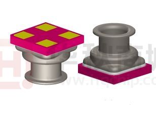
The LPS33K has a unique cylindrical package solution with a full metal lid assembled on ceramic substrate and
this cylindrical package provides an easy assembly with O-rings in the end user’s application.
Figure 4. LPS33K internal structure
This structure (Figure 4) is to show the inner structure of the LPS33K with a metal lid and potting gel. This
structure is designed for and proven to protect electronic components from long-term exposure to harsh
environments such as water mixed with chlorine, bromine, commercial washing detergent and fuels, solvents and
chemicals. It also provides excellent low-stress encapsulation performance for sensitive electronic components
from severe environmental conditions such as high temperature and humidity, refer to the properties of the gel
which are given in the following table.
Table 7. Potting gel properties
Properties
Permeability g/m²·24 hr
7
Hardness (penetration) based on ASTM D1403
70
Ultra-low Young's modulus
TCE (Thermal Coefficient of Expansion)
DS12817 - Rev 3
Potting gel
Less than 0.01 GPa
300 ppm/°C
page 8/31
�LPS33K
Interpreting pressure readings
3.5
Interpreting pressure readings
The pressure data are stored 3 registers: PRESS_OUT_H (2Ah), PRESS_OUT_L (29h), and PRESS_OUT_XL
(28h). The value is expressed as 2’s complement.
To obtain the pressure in hPa, take the two’s complement of the complete word and then divide by 4096 LSB/hPa.
Figure 5. Pressure readings
DS12817 - Rev 3
page 9/31
�LPS33K
Application hints
4
Application hints
Figure 6. LPS33K electrical connections (bottom view)
GND
SDA
4
1
SCL
3
2
VDD
C1
GND
The device power supply must be provided through the VDD line; a power supply decoupling capacitor C1 (100
nF) must be placed as near as possible to the supply pads of the device. Depending on the application, an
additional capacitor of 4.7 µF could be placed on the VDD line.
The functionality of the device and the measured data outputs are selectable and accessible through the I²C
interface.
All the voltage and ground supplies must be present at the same time to have proper behavior of the IC (refer to
Figure 6).
Figure 7. LPS33K power-off sequence
VDD
0.2V
Min.10ms
Time
DS12817 - Rev 3
VDD Rising / Falling time : 10 µs ~ 100 ms
VDD must be lower than 0.2 V for at least 10 ms during power-off sequence for correct POR
page 10/31
�LPS33K
Soldering information
4.1
Soldering information
The CCLGA package is compliant with the ECOPACK standard and it is qualified for soldering heat resistance
according to JEDEC J-STD-020.
DS12817 - Rev 3
page 11/31
�LPS33K
Digital interfaces
5
Digital interfaces
5.1
IC serial interface
The registers embedded in the LPS33K may be accessed through the I²C interface.
Table 8. Serial interface pin description
Pin name
5.2
Pin description
SCL
I²C serial clock (SCL)
SDA
I²C serial data (SDA)
I²C serial interface
The LPS33K I²C is a bus slave. The I²C is employed to write data into registers whose content can also be read
back.
The relevant I²C terminology is given in the following table.
Table 9. I²C terminology
Term
Transmitter
Receiver
Description
The device which sends data to the bus
The device which receives data from the bus
Master
The device which initiates a transfer, generates clock signals and terminates a transfer
Slave
The device addressed by the master
There are two signals associated with the I²C bus: the serial clock line (SCL) and the serial data line (SDA). The
latter is a bidirectional line used for sending and receiving the data to/from the interface. Both lines have to be
connected to VDD through pull-up resistors.
The I²C interface is compliant with fast mode (400 kHz) I²C standards as well as with the normal mode.
DS12817 - Rev 3
page 12/31
�LPS33K
I²C serial interface
5.2.1
I²C operation
The transaction on the bus is started through a START (ST) signal. A start condition is defined as a HIGH-to-LOW
transition on the data line while the SCL line is held HIGH. After this has been transmitted by the master, the bus
is considered busy. The next data byte transmitted after the start condition contains the address of the slave in the
first 7 bits and the eighth bit tells whether the master is receiving data from the slave or transmitting data to the
slave. When an address is sent, each device in the system compares the first seven bits after a start condition
with its address. If they match, the device considers itself addressed by the master.
The slave address (SAD) associated to the LPS33K is 1011101b.
Data transfer with acknowledge is mandatory. The transmitter must release the SDA line during the acknowledge
pulse. The receiver must then pull the data line LOW so that it remains stable low during the HIGH period of the
acknowledge clock pulse. A receiver which has been addressed is obliged to generate an acknowledge after each
byte of data received.
The I²C embedded inside the ASIC behaves like a slave device and the following protocol must be adhered to.
After the start condition (ST) a slave address is sent, once a slave acknowledge has been returned (SAK), an 8bit sub-address will be transmitted (SUB): the 7 LSB represent the actual register address while the MSB has no
meaning. The IF_ADD_INC bit in CTRL_REG2 (11h) enables sub-address auto increment (IF_ADD_INC is '1' by
default), so if IF_ADD_INC = '1' the SUB (sub-address) will be automatically increased to allow multiple data read/
write.
The slave address is completed with a Read/Write bit. If the bit is ‘1’ (Read), a repeated START (SR) condition
must be issued after the two sub-address bytes; if the bit is ‘0’ (Write) the master will transmit to the slave with
direction unchanged. The following table explains how the SAD+read/write bit pattern is composed, listing all the
possible configurations.
Table 10. SAD+Read/Write patterns
Command
SAD[6:0]
R/W
SAD+R/W
Read
1011101
1
10111011 (BBh)
Write
1011101
0
10111010 (BAh)
Table 11. Transfer when master is writing one byte to slave
Master
ST
SAD + W
SUB
Slave
DATA
SAK
SP
SAK
SAK
Table 12. Transfer when master is writing multiple bytes to slave
Master
ST
SAD + W
SUB
Slave
SAK
DATA
SAK
DATA
SP
SAK
SAK
Table 13. Transfer when master is receiving (reading) one byte of data from slave
Master
ST
SAD + W
Slave
SUB
SAK
SR
SAD + R
SAK
NMAK
SAK
SP
DATA
Table 14. Transfer when master is receiving (reading) multiple bytes of data from slave
Master
ST
Slave
DS12817 - Rev 3
SAD+W
SUB
SAK
SR
SAK
SAD+R
MAK
SAK
DATA
MAK
DATA
NMAK
SP
DATA
page 13/31
�LPS33K
I²C serial interface
Data are transmitted in byte format (DATA). Each data transfer contains 8 bits. The number of bytes transferred
per transfer is unlimited. Data is transferred with the most significant bit (MSb) first. If a slave receiver does not
acknowledge the slave address (i.e. it is not able to receive because it is performing some real-time function) the
data line must be kept HIGH by the slave. The master can then abort the transfer. A LOW-to-HIGH transition on
the SDA line while the SCL line is HIGH is defined as a STOP condition. Each data transfer must be terminated
by the generation of a STOP (SP) condition.
In the presented communication format MAK is master acknowledge and NMAK is no master acknowledge.
DS12817 - Rev 3
page 14/31
�LPS33K
Register map
6
Register map
The following table provides a quick overview of the 8-bit registers embedded in the device.
Table 15. Registers address map
Register
Name
Type
Address
Hex
Default
Function and comment
Binary
Reserved
-
00-0E
-
Reserved
WHO_AM_I
R
0F
10110001
Who am I
CTRL_REG1
R/W
10
00000000
CTRL_REG2
R/W
11
00010000
CTRL_REG3
R/W
Reserved
12
00000000
13-17
-
Control registers
Reserved
RPDS_L
R/W
18
00000000
RPDS_H
R/W
19
00000000
RES_CONF
R/W
1A
00000000
Resolution register
Reserved
-
1B-26
-
Reserved
STATUS
R
27
output
Status register
PRESS_OUT_XL
R
28
output
PRESS_OUT_L
R
29
output
PRESS_OUT_H
R
2A
output
TEMP_OUT_L
R
2B
output
TEMP_OUT_H
R
2C
output
Reserved
-
2D-32
-
Reserved
LPFP_RES
R
33
output
Filter reset register
Pressure offset registers
Pressure output registers
Temperature output registers
Registers marked as Reserved must not be changed. Writing to those registers may cause permanent damage to
the device.
To guarantee the proper behavior of the device, all register addresses not listed in the above table must not be
accessed and the content stored in those registers must not be changed.
The content of the registers that are loaded at boot should not be changed. They contain the factory calibration
values. Their content is automatically restored when the device is powered up.
DS12817 - Rev 3
page 15/31
�LPS33K
Register description
7
Register description
The device contains a set of registers which are used to control its behavior and to retrieve pressure and
temperature data. The register address, made up of 7 bits, is used to identify them and to read/write the data
through the serial interface.
7.1
WHO_AM_I (0Fh)
Device Who am I
7.2
7
6
5
4
3
2
1
0
1
0
1
1
0
0
0
1
CTRL_REG1 (10h)
Control register 1
7
6
5
4
3
2
1
0
0(1)
ODR2
ODR1
ODR0
EN_LPFP
LPFP_CFG
BDU
0(1)
1. This bit must be set to ‘0’ for proper operation of the device.
ODR[2:0]
EN_LPFP
LPFP_CFG
Output data rate selection. Default value: 000
Refer to Table 16.
Enable low-pass filter on pressure data. Default value: 0
(0: low-pass filter disabled; 1: low-pass filter enabled)
Low-pass configuration register. Default value: 0
Refer to Table 17.
Block data update. Default value: 0
BDU(1)
(0: continuous update;
1: output registers not updated until MSB and LSB have been read)
1. To guarantee the correct behavior of the BDU feature, PRESS_OUT_H (2Ah) must be the last address read.
Table 16. Output data rate bit configurations
DS12817 - Rev 3
ODR2
ODR1
ODR0
0
0
0
0
0
1
1 Hz
1 Hz
0
1
0
10 Hz
10 Hz
0
1
1
25 Hz
25 Hz
1
0
0
50 Hz
50 Hz
1
0
1
75 Hz
75 Hz
Pressure (Hz)
Temperature (Hz)
Power down / one-shot mode enabled
page 16/31
�LPS33K
CTRL_REG1 (10h)
When the ODR bits are set to '000' the device is in Power-down mode. When the device is in power-down mode,
almost all internal blocks of the device are switched off to minimize power consumption. The I²C interface is still
active to allow communication with the device. The content of the configuration registers is preserved and output
data registers are not updated, therefore keeping the last data sampled in memory before going into power-down
mode.
If the ONE_SHOT bit in CTRL_REG2 (11h) is set to '1', One-shot mode is triggered and a new acquisition starts
when it is required. Enabling this mode is possible only if the device was previously in power-down mode (ODR
bits set to '000'). Once the acquisition is completed and the output registers updated, the device automatically
enters in power-down mode. The ONE_SHOT bit self-clears itself.
When the ODR bits are set to a value different than '000', the device is in Continuous mode and automatically
acquires a set of data (pressure and temperature) at the frequency selected through the ODR[2:0] bits.
Once the additional low-pass filter has been enabled through the EN_LPFP bit, it is possible to configure the
device bandwidth acting on the LPFP_CFG bit. Refer to the following table for low-pass filter configurations.
Table 17. Low-pass filter configurations
EN_LPFP
LPFP_CFG
Additional low-pass filter status
Device bandwidth
0
x
Disabled
ODR/2
1
0
Enabled
ODR/9
1
1
Enabled
ODR/20
The BDU bit is used to inhibit the update of the output registers between the reading of the upper and lower
register parts. In default mode (BDU = ‘0’), the lower and upper register parts are updated continuously. When the
BDU is activated (BDU = ‘1’), the content of the output registers is not updated until PRESS_OUT_H (2Ah) is
read, in order to avoid reading values related to different samples.
DS12817 - Rev 3
page 17/31
�LPS33K
CTRL_REG2 (11h)
7.3
CTRL_REG2 (11h)
Control register 2
7
6
5
BOOT
0(1)
0(1)
4
3
IF_ADD_INC
0(1)
2
1
0
SWRESET
0(1)
ONE_SHOT
1. This bit must be set to ‘0’ for proper operation of the device.
Reboot memory content. Default value: 0
BOOT
(0: normal mode; 1: reboot memory content).
The bit is self-cleared when the BOOT is completed.
Register address automatically incremented during a multiple byte access with a serial interface (I²C).
IF_ADD_INC
Default value: 1
(0: disable; 1 enable)
Software reset. Default value: 0
SWRESET
(0: normal mode; 1: software reset).
The bit is self-cleared when the reset is completed.
ONE_SHOT
One-shot enable. Default value: 0
(0: idle mode; 1: a new dataset is acquired)
The BOOT bit is used to refresh the content of the internal registers stored in the Flash memory block. At device
power-up the content of the Flash memory block is transferred to the internal registers related to the trimming
functions to allow correct behavior of the device itself. If for any reason the content of the trimming registers is
modified, it is sufficient to use this bit to restore the correct values. When the BOOT bit is set to ‘1’, the content of
the internal Flash is copied inside the corresponding internal registers and is used to calibrate the device. These
values are factory trimmed and they are different for every device. They allow correct behavior of the device and
normally they should not be changed. At the end of the boot process the BOOT bit is set again to ‘0’ by hardware.
The BOOT bit takes effect after one ODR clock cycle.
The IF_ADD_INC bit is enabled to increment the register address automatically during a multiple byte access with
I²C. In order to read the data properly on multiple byte and single byte access, the recommended configuration for
the LPS33K is the following.
•
For multiple byte access, synchronous data reading is only allowed with IF_ADD_INC = 1 and BDU = 0;
•
For single byte access, either synchronous or asynchronous can be used with IF_ADD_INC = 0, but BDU
has to be set to "1" for asynchronous data reading.
SWRESET is the software reset bit. The following device registers (CTRL_REG1 (10h), CTRL_REG2 (11h)) are
reset to the default value if the SWRESET bit is set to '1'. The SWRESET bit returns back to '0' by hardware.
The ONE_SHOT bit is used to start a new conversion when the ODR[2:0] bits in CTRL_REG1 (10h) are set to
‘000’. Writing a ‘1’ in ONE_SHOT triggers a single measurement of pressure and temperature. Once the
measurement is done, the ONE_SHOT bit will self-clear, the new data are available in the output registers, and
the STATUS (27h) bits are updated.
DS12817 - Rev 3
page 18/31
�LPS33K
RPDS_L (18h)
7.4
RPDS_L (18h)
Pressure offset (LSB data)
7
6
5
4
3
2
1
0
RPDS7
RPDS6
RPDS5
RPDS4
RPDS3
RPDS2
RPDS1
RPDS0
RPDS[7:0]
This register contains the low part of the pressure offset value.
If, after the soldering of the component, a residual offset is still present, it can be removed with a one-point
calibration.
After soldering, the measured offset can be stored in the RPDS_H (19h) and RPDS_L (18h) registers and
automatically subtracted from the pressure output registers: the output pressure register PRESS_OUT (28h, 29h
and 2Ah) is provided as the difference between the measured pressure and the content of the register 256*RPDS
(18h, 19h).
7.5
RPDS_H (19h)
Pressure offset (MSB data)
7
6
5
4
3
2
1
0
RPDS15
RPDS14
RPDS13
RPDS12
RPDS11
RPDS10
RPDS9
RPDS8
RPDS[15:8]
7.6
This register contains the high part of the pressure offset value. Refer to RPDS_L (18h).
RES_CONF (1Ah)
Low-power mode configuration
7
6
5
4
3
2
1
0
0(1)
0(1)
0(1)
0(1)
0(1)
0(1)
reserved(2)
LC_EN
1. This bit must be set to ‘0’ for proper operation of the device.
2. The content of this bit must not be modified for proper operation of the device.
LC_EN(1)
Low-current mode enable. Default: 0
(0: normal mode (low-noise mode); 1: low-current mode).
1. The LC_EN bit must be changed only with the device in power down and not during operation. Once the LC_EN bit is
configured, it affects both One-shot mode and Continuous mode.
DS12817 - Rev 3
page 19/31
�LPS33K
STATUS (27h)
7.7
STATUS (27h)
Status register
7
6
5
4
3
2
1
0
-
-
T_OR
P_OR
-
-
T_DA
P_DA
Temperature data overrun.
T_OR
(0: no overrun has occurred;
1: new data for temperature has overwritten the previous data)
Pressure data overrun.
P_OR
(0: no overrun has occurred;
1: new data for pressure has overwritten the previous data)
Temperature data available.
T_DA
(0: new data for temperature is not yet available;
1: new data for temperature is available)
Pressure data available.
P_DA
(0: new data for pressure is not yet available;
1: new data for pressure is available)
This register is updated every ODR cycle.
7.8
PRESS_OUT_XL (28h)
Pressure output value (LSB)
7
6
5
4
3
2
1
0
POUT7
POUT6
POUT5
POUT4
POUT3
POUT2
POUT1
POUT0
POUT[7:0]
This register contains the low part of the pressure output value.
The pressure output value is 24-bit data that contains the measured pressure. It is composed of PRESS_OUT_H
(2Ah), PRESS_OUT_L (29h) and PRESS_OUT_XL (28h). The value is expressed as 2’s complement.
The output pressure register PRESS_OUT is provided as the difference between the measured pressure and the
content of the register RPDS (18h, 19h).
Please refer to Section 3.5 Interpreting pressure readings for additional info.
DS12817 - Rev 3
page 20/31
�LPS33K
PRESS_OUT_L (29h)
7.9
PRESS_OUT_L (29h)
Pressure output value (mid part)
7
6
5
4
3
2
1
0
POUT15
POUT14
POUT13
POUT12
POUT11
POUT10
POUT9
POUT8
POUT[15:8]
7.10
This register contains the mid part of the pressure output value. Refer to PRESS_OUT_XL (28h).
PRESS_OUT_H (2Ah)
Pressure output value (MSB)
7
6
5
4
3
2
1
0
POUT23
POUT22
POUT21
POUT20
POUT19
POUT18
POUT17
POUT16
POUT[23:16]
7.11
This register contains the high part of the pressure output value. Refer to PRESS_OUT_XL (28h).
TEMP_OUT_L (2Bh)
Temperature output value (LSB)
7
6
5
4
3
2
1
0
TOUT7
TOUT6
TOUT5
TOUT4
TOUT3
TOUT2
TOUT1
TOUT0
TOUT[7:0]
This register contains the low part of the temperature output value.
The temperature output value is 16-bit data that contains the measured temperature. It is composed of
TEMP_OUT_H (2Ch) and TEMP_OUT_L (2Bh). The value is expressed as 2’s complement.
DS12817 - Rev 3
page 21/31
�LPS33K
TEMP_OUT_H (2Ch)
7.12
TEMP_OUT_H (2Ch)
Temperature output value (MSB)
7
6
5
4
3
2
1
0
TOUT15
TOUT14
TOUT13
TOUT12
TOUT11
TOUT10
TOUT9
TOUT8
TOUT[15:8]
This register contains the high part of the temperature output value.
The temperature output value is 16-bit data that contains the measured temperature. It is composed of
TEMP_OUT_H (2Ch) and TEMP_OUT_L (2Bh). The value is expressed as 2’s complement.
7.13
LPFP_RES (33h)
Low-pass filter reset register.
If the LPFP is active, in order to avoid the transitory phase, the filter can be reset by reading this register before
generating pressure measurements.
DS12817 - Rev 3
page 22/31
�LPS33K
Package information
8
Package information
In order to meet environmental requirements, ST offers these devices in different grades of ECOPACK packages,
depending on their level of environmental compliance. ECOPACK specifications, grade definitions and product
status are available at: www.st.com. ECOPACK is an ST trademark.
8.1
CCLGA 4L package information
Figure 8. CCLGA - 4L (3.3 x 3.3 x max 2.9 mm) package outline and mechanical data
Dimensions are in millimeter unless otherwise specified
General Tolerance is +/-0.10mm unless otherwise specified
OUTER DIMENSIONS
ITEM
Length [L]
W idth [W ]
Height [H]
DIMENSION [mm]
3.3
3.3
2.9 MAX
TOLERANCE [mm]
±0.15
±0.15
/
DM00547458_1
DS12817 - Rev 3
page 23/31
�LPS33K
CCLGA 4L packing information
8.2
CCLGA 4L packing information
Figure 9. Carrier tape information for CCLGA 4L package
Figure 10. Package orientation in carrier tape
DS12817 - Rev 3
page 24/31
�LPS33K
CCLGA 4L packing information
Figure 11. Reel information carrier tape CCLGA 4L
T
40mm min.
Access hole at
slot location
B
C
N
D
A
Full radius
G measured at hub
Tape slot
in core for
tape start
2.5mm min. width
Table 18. Reel dimensions for carrier tape of CCLGA 4L package
Reel dimensions (mm)
DS12817 - Rev 3
A (max)
330
B (min)
1.5
C
13 ±0.25
D (min)
20.2
N (min)
60
G
12.4 +2/-0
T (max)
18.4
page 25/31
�LPS33K
Revision history
Table 19. Document revision history
DS12817 - Rev 3
Date
Version
20-May-2020
3
Changes
First public release
page 26/31
�LPS33K
Contents
Contents
1
Block diagram and pin description . . . . . . . . . . . . . . . . . . . . . . . . . . . . . . . . . . . . . . . . . . . . . . . . . 2
2
Mechanical and electrical specifications . . . . . . . . . . . . . . . . . . . . . . . . . . . . . . . . . . . . . . . . . . . 3
2.1
Mechanical characteristics . . . . . . . . . . . . . . . . . . . . . . . . . . . . . . . . . . . . . . . . . . . . . . . . . . . . . . . 3
2.2
Electrical characteristics. . . . . . . . . . . . . . . . . . . . . . . . . . . . . . . . . . . . . . . . . . . . . . . . . . . . . . . . . 4
2.3
Communication interface characteristics . . . . . . . . . . . . . . . . . . . . . . . . . . . . . . . . . . . . . . . . . . . 5
2.3.1
2.4
3
4
Absolute maximum ratings. . . . . . . . . . . . . . . . . . . . . . . . . . . . . . . . . . . . . . . . . . . . . . . . . . . . . . . 6
Functionality . . . . . . . . . . . . . . . . . . . . . . . . . . . . . . . . . . . . . . . . . . . . . . . . . . . . . . . . . . . . . . . . . . . . . .7
3.1
Sensing element . . . . . . . . . . . . . . . . . . . . . . . . . . . . . . . . . . . . . . . . . . . . . . . . . . . . . . . . . . . . . . . 7
3.2
IC interface. . . . . . . . . . . . . . . . . . . . . . . . . . . . . . . . . . . . . . . . . . . . . . . . . . . . . . . . . . . . . . . . . . . . 7
3.3
Factory calibration. . . . . . . . . . . . . . . . . . . . . . . . . . . . . . . . . . . . . . . . . . . . . . . . . . . . . . . . . . . . . . 7
3.4
Device structure . . . . . . . . . . . . . . . . . . . . . . . . . . . . . . . . . . . . . . . . . . . . . . . . . . . . . . . . . . . . . . . 8
3.5
Interpreting pressure readings. . . . . . . . . . . . . . . . . . . . . . . . . . . . . . . . . . . . . . . . . . . . . . . . . . . . 9
Application hints . . . . . . . . . . . . . . . . . . . . . . . . . . . . . . . . . . . . . . . . . . . . . . . . . . . . . . . . . . . . . . . . .10
4.1
5
I²C - inter-IC control interface . . . . . . . . . . . . . . . . . . . . . . . . . . . . . . . . . . . . . . . . . . . . . . . 5
Soldering information . . . . . . . . . . . . . . . . . . . . . . . . . . . . . . . . . . . . . . . . . . . . . . . . . . . . . . . . . . 11
Digital interfaces . . . . . . . . . . . . . . . . . . . . . . . . . . . . . . . . . . . . . . . . . . . . . . . . . . . . . . . . . . . . . . . . .12
5.1
IC serial interface . . . . . . . . . . . . . . . . . . . . . . . . . . . . . . . . . . . . . . . . . . . . . . . . . . . . . . . . . . . . . 12
5.2
I²C serial interface . . . . . . . . . . . . . . . . . . . . . . . . . . . . . . . . . . . . . . . . . . . . . . . . . . . . . . . . . . . . . 12
5.2.1
I²C operation . . . . . . . . . . . . . . . . . . . . . . . . . . . . . . . . . . . . . . . . . . . . . . . . . . . . . . . . . . . 13
6
Register map . . . . . . . . . . . . . . . . . . . . . . . . . . . . . . . . . . . . . . . . . . . . . . . . . . . . . . . . . . . . . . . . . . . . .15
7
Register description . . . . . . . . . . . . . . . . . . . . . . . . . . . . . . . . . . . . . . . . . . . . . . . . . . . . . . . . . . . . . .16
7.1
WHO_AM_I (0Fh) . . . . . . . . . . . . . . . . . . . . . . . . . . . . . . . . . . . . . . . . . . . . . . . . . . . . . . . . . . . . . 16
7.2
CTRL_REG1 (10h) . . . . . . . . . . . . . . . . . . . . . . . . . . . . . . . . . . . . . . . . . . . . . . . . . . . . . . . . . . . . 16
7.3
CTRL_REG2 (11h) . . . . . . . . . . . . . . . . . . . . . . . . . . . . . . . . . . . . . . . . . . . . . . . . . . . . . . . . . . . . 18
7.4
RPDS_L (18h) . . . . . . . . . . . . . . . . . . . . . . . . . . . . . . . . . . . . . . . . . . . . . . . . . . . . . . . . . . . . . . . . 19
7.5
RPDS_H (19h). . . . . . . . . . . . . . . . . . . . . . . . . . . . . . . . . . . . . . . . . . . . . . . . . . . . . . . . . . . . . . . . 19
7.6
RES_CONF (1Ah). . . . . . . . . . . . . . . . . . . . . . . . . . . . . . . . . . . . . . . . . . . . . . . . . . . . . . . . . . . . . 19
7.7
STATUS (27h) . . . . . . . . . . . . . . . . . . . . . . . . . . . . . . . . . . . . . . . . . . . . . . . . . . . . . . . . . . . . . . . . 20
7.8
PRESS_OUT_XL (28h) . . . . . . . . . . . . . . . . . . . . . . . . . . . . . . . . . . . . . . . . . . . . . . . . . . . . . . . . 20
DS12817 - Rev 3
page 27/31
�LPS33K
Contents
8
7.9
PRESS_OUT_L (29h). . . . . . . . . . . . . . . . . . . . . . . . . . . . . . . . . . . . . . . . . . . . . . . . . . . . . . . . . . 21
7.10
PRESS_OUT_H (2Ah) . . . . . . . . . . . . . . . . . . . . . . . . . . . . . . . . . . . . . . . . . . . . . . . . . . . . . . . . . 21
7.11
TEMP_OUT_L (2Bh) . . . . . . . . . . . . . . . . . . . . . . . . . . . . . . . . . . . . . . . . . . . . . . . . . . . . . . . . . . 21
7.12
TEMP_OUT_H (2Ch) . . . . . . . . . . . . . . . . . . . . . . . . . . . . . . . . . . . . . . . . . . . . . . . . . . . . . . . . . . 22
7.13
LPFP_RES (33h). . . . . . . . . . . . . . . . . . . . . . . . . . . . . . . . . . . . . . . . . . . . . . . . . . . . . . . . . . . . . . 22
Package information. . . . . . . . . . . . . . . . . . . . . . . . . . . . . . . . . . . . . . . . . . . . . . . . . . . . . . . . . . . . . .23
8.1
CCLGA 4L package information . . . . . . . . . . . . . . . . . . . . . . . . . . . . . . . . . . . . . . . . . . . . . . . . . 23
8.2
CCLGA 4L packing information . . . . . . . . . . . . . . . . . . . . . . . . . . . . . . . . . . . . . . . . . . . . . . . . . . 24
Revision history . . . . . . . . . . . . . . . . . . . . . . . . . . . . . . . . . . . . . . . . . . . . . . . . . . . . . . . . . . . . . . . . . . . . . . .26
Contents . . . . . . . . . . . . . . . . . . . . . . . . . . . . . . . . . . . . . . . . . . . . . . . . . . . . . . . . . . . . . . . . . . . . . . . . . . . . . .27
List of tables . . . . . . . . . . . . . . . . . . . . . . . . . . . . . . . . . . . . . . . . . . . . . . . . . . . . . . . . . . . . . . . . . . . . . . . . . .29
List of figures. . . . . . . . . . . . . . . . . . . . . . . . . . . . . . . . . . . . . . . . . . . . . . . . . . . . . . . . . . . . . . . . . . . . . . . . . .30
DS12817 - Rev 3
page 28/31
�LPS33K
List of tables
List of tables
Table 1.
Table 2.
Table 3.
Table 4.
Table 5.
Table 6.
Table 7.
Table 8.
Table 9.
Table 10.
Table 11.
Table 12.
Table 13.
Table 14.
Table 15.
Table 16.
Table 17.
Table 18.
Table 19.
Pin description. . . . . . . . . . . . . . . . . . . . . . . . . . . . . . . . . . . . . . . . . . . .
Pressure and temperature sensor characteristics . . . . . . . . . . . . . . . . . . . .
Electrical characteristics . . . . . . . . . . . . . . . . . . . . . . . . . . . . . . . . . . . . .
DC characteristics . . . . . . . . . . . . . . . . . . . . . . . . . . . . . . . . . . . . . . . . .
I²C slave timing values . . . . . . . . . . . . . . . . . . . . . . . . . . . . . . . . . . . . . .
Absolute maximum ratings . . . . . . . . . . . . . . . . . . . . . . . . . . . . . . . . . . .
Potting gel properties . . . . . . . . . . . . . . . . . . . . . . . . . . . . . . . . . . . . . . .
Serial interface pin description . . . . . . . . . . . . . . . . . . . . . . . . . . . . . . . . .
I²C terminology . . . . . . . . . . . . . . . . . . . . . . . . . . . . . . . . . . . . . . . . . . .
SAD+Read/Write patterns . . . . . . . . . . . . . . . . . . . . . . . . . . . . . . . . . . . .
Transfer when master is writing one byte to slave. . . . . . . . . . . . . . . . . . . .
Transfer when master is writing multiple bytes to slave . . . . . . . . . . . . . . . .
Transfer when master is receiving (reading) one byte of data from slave . . . .
Transfer when master is receiving (reading) multiple bytes of data from slave
Registers address map . . . . . . . . . . . . . . . . . . . . . . . . . . . . . . . . . . . . . .
Output data rate bit configurations . . . . . . . . . . . . . . . . . . . . . . . . . . . . . .
Low-pass filter configurations . . . . . . . . . . . . . . . . . . . . . . . . . . . . . . . . .
Reel dimensions for carrier tape of CCLGA 4L package . . . . . . . . . . . . . . .
Document revision history . . . . . . . . . . . . . . . . . . . . . . . . . . . . . . . . . . . .
DS12817 - Rev 3
.
.
.
.
.
.
.
.
.
.
.
.
.
.
.
.
.
.
.
.
.
.
.
.
.
.
.
.
.
.
.
.
.
.
.
.
.
.
.
.
.
.
.
.
.
.
.
.
.
.
.
.
.
.
.
.
.
.
.
.
.
.
.
.
.
.
.
.
.
.
.
.
.
.
.
.
.
.
.
.
.
.
.
.
.
.
.
.
.
.
.
.
.
.
.
.
.
.
.
.
.
.
.
.
.
.
.
.
.
.
.
.
.
.
.
.
.
.
.
.
.
.
.
.
.
.
.
.
.
.
.
.
.
.
.
.
.
.
.
.
.
.
.
.
.
.
.
.
.
.
.
.
.
.
.
.
.
.
.
.
.
.
.
.
.
.
.
.
.
.
.
.
.
.
.
.
.
.
.
.
.
.
.
.
.
.
.
.
.
.
.
.
.
.
.
.
.
.
.
.
.
.
.
.
.
.
.
.
.
.
.
.
.
.
.
.
.
.
.
.
.
.
.
.
.
.
.
.
.
.
.
.
.
.
.
.
.
.
.
.
.
.
.
.
.
.
.
.
.
.
.
.
.
.
.
.
.
.
.
.
.
.
.
.
.
.
.
.
.
.
.
.
.
.
.
.
.
.
.
.
.
.
.
.
.
.
.
.
.
.
.
.
.
.
.
.
.
.
.
.
.
.
.
.
.
.
.
.
.
.
.
.
.
.
.
.
.
.
.
.
.
.
.
.
.
.
.
.
.
.
.
.
.
.
.
.
.
.
.
.
.
.
.
.
.
.
.
.
.
.
.
.
.
.
.
.
.
.
.
.
.
.
.
.
.
.
.
.
.
.
.
.
.
.
.
.
.
.
.
.
.
.
.
.
.
.
.
.
.
.
.
.
.
.
.
.
.
.
.
.
.
.
.
.
.
.
.
.
.
.
.
.
.
.
.
.
.
.
.
.
.
.
.
.
.
.
.
.
.
.
.
.
.
.
.
.
.
.
.
.
.
.
.
.
.
.
.
.
.
.
.
.
.
.
.
.
.
.
.
.
.
.
.
.
.
.
.
.
.
.
.
.
.
.
.
. 2
. 3
. 4
. 4
. 5
. 6
. 8
12
12
13
13
13
13
13
15
16
17
25
26
page 29/31
�LPS33K
List of figures
List of figures
Figure 1.
Figure 2.
Figure 3.
Figure 4.
Figure 5.
Figure 6.
Figure 7.
Figure 8.
Figure 9.
Figure 10.
Figure 11.
DS12817 - Rev 3
Block diagram . . . . . . . . . . . . . . . . . . . . . . . . . . . . . . . . . . . . . . . . . . .
Pin connections (bottom view) . . . . . . . . . . . . . . . . . . . . . . . . . . . . . . . .
I²C slave timing diagram . . . . . . . . . . . . . . . . . . . . . . . . . . . . . . . . . . . .
LPS33K internal structure . . . . . . . . . . . . . . . . . . . . . . . . . . . . . . . . . . .
Pressure readings. . . . . . . . . . . . . . . . . . . . . . . . . . . . . . . . . . . . . . . . .
LPS33K electrical connections (bottom view) . . . . . . . . . . . . . . . . . . . . . .
LPS33K power-off sequence . . . . . . . . . . . . . . . . . . . . . . . . . . . . . . . . .
CCLGA - 4L (3.3 x 3.3 x max 2.9 mm) package outline and mechanical data
Carrier tape information for CCLGA 4L package . . . . . . . . . . . . . . . . . . . .
Package orientation in carrier tape . . . . . . . . . . . . . . . . . . . . . . . . . . . . .
Reel information carrier tape CCLGA 4L . . . . . . . . . . . . . . . . . . . . . . . . .
.
.
.
.
.
.
.
.
.
.
.
.
.
.
.
.
.
.
.
.
.
.
.
.
.
.
.
.
.
.
.
.
.
.
.
.
.
.
.
.
.
.
.
.
.
.
.
.
.
.
.
.
.
.
.
.
.
.
.
.
.
.
.
.
.
.
.
.
.
.
.
.
.
.
.
.
.
.
.
.
.
.
.
.
.
.
.
.
.
.
.
.
.
.
.
.
.
.
.
.
.
.
.
.
.
.
.
.
.
.
.
.
.
.
.
.
.
.
.
.
.
.
.
.
.
.
.
.
.
.
.
.
.
.
.
.
.
.
.
.
.
.
.
.
.
.
.
.
.
.
.
.
.
.
.
.
.
.
.
.
.
.
.
.
.
.
.
.
.
.
.
.
.
.
.
.
.
.
.
.
.
.
.
.
.
.
.
.
.
.
.
.
.
.
.
.
.
.
.
.
.
.
.
.
.
.
.
.
.
.
.
.
.
.
.
.
.
.
.
.
.
.
.
.
.
.
.
.
.
.
.
.
.
.
.
.
.
.
.
.
.
.
.
.
.
.
.
.
.
.
.
.
.
.
.
.
.
.
.
.
.
.
.
.
. 2
. 2
. 5
. 8
. 9
10
10
23
24
24
25
page 30/31
�LPS33K
IMPORTANT NOTICE – PLEASE READ CAREFULLY
STMicroelectronics NV and its subsidiaries (“ST”) reserve the right to make changes, corrections, enhancements, modifications, and improvements to ST
products and/or to this document at any time without notice. Purchasers should obtain the latest relevant information on ST products before placing orders. ST
products are sold pursuant to ST’s terms and conditions of sale in place at the time of order acknowledgement.
Purchasers are solely responsible for the choice, selection, and use of ST products and ST assumes no liability for application assistance or the design of
Purchasers’ products.
No license, express or implied, to any intellectual property right is granted by ST herein.
Resale of ST products with provisions different from the information set forth herein shall void any warranty granted by ST for such product.
ST and the ST logo are trademarks of ST. For additional information about ST trademarks, please refer to www.st.com/trademarks. All other product or service
names are the property of their respective owners.
Information in this document supersedes and replaces information previously supplied in any prior versions of this document.
© 2020 STMicroelectronics – All rights reserved
DS12817 - Rev 3
page 31/31
�