M24128S-FCU
128-Kbit serial I²C bus EEPROM 4 balls CSP
Datasheet - preliminary data
Features
•
Compatible with the 400 kHz I²C protocol
• Memory array:
– 128 Kbits (16 Kbytes) of EEPROM
– Page size: 32 bytes
• Supply voltage range:
– 1.7 V to 5.5 V
WLCSP (CU)
• Operating temperature range
– Read: -40 °C/+85 °C
– Write: 0 °C/+85 °C
• Write
– Byte Write within 5 ms
– Page Write within 5 ms
• Random and sequential read modes
• Software Write protect
– Upper quarter memory array
– Upper half memory array
– Upper 3/4 memory array
– Whole memory array
• ESD protection
– Human Body Model: 4 kV
• More than 1 million Write cycles
• More than 40-years data retention
• Package
– WLCSP, RoHS and Halogen free compliant
(ECOPACK®2)
June 2014
DocID025717 Rev 3
This is preliminary information on a new product now in development or undergoing evaluation. Details are subject to
change without notice.
1/30
www.st.com
�Contents
M24128S-FCU
Contents
1
Description . . . . . . . . . . . . . . . . . . . . . . . . . . . . . . . . . . . . . . . . . . . . . . . . . 6
2
Signal description . . . . . . . . . . . . . . . . . . . . . . . . . . . . . . . . . . . . . . . . . . . 7
2.1
Serial Clock (SCL) . . . . . . . . . . . . . . . . . . . . . . . . . . . . . . . . . . . . . . . . . . . 7
2.2
Serial Data (SDA) . . . . . . . . . . . . . . . . . . . . . . . . . . . . . . . . . . . . . . . . . . . . 7
2.3
VSS (ground) . . . . . . . . . . . . . . . . . . . . . . . . . . . . . . . . . . . . . . . . . . . . . . . 7
2.4
Supply voltage (VCC) . . . . . . . . . . . . . . . . . . . . . . . . . . . . . . . . . . . . . . . . . 7
2.4.1
Operating supply voltage (VCC) . . . . . . . . . . . . . . . . . . . . . . . . . . . . . . . . 7
2.4.2
Power-up conditions . . . . . . . . . . . . . . . . . . . . . . . . . . . . . . . . . . . . . . . . 7
2.4.3
Device reset . . . . . . . . . . . . . . . . . . . . . . . . . . . . . . . . . . . . . . . . . . . . . . . 7
2.4.4
Power-down conditions . . . . . . . . . . . . . . . . . . . . . . . . . . . . . . . . . . . . . . 8
3
Memory organization . . . . . . . . . . . . . . . . . . . . . . . . . . . . . . . . . . . . . . . . 9
4
Device operation . . . . . . . . . . . . . . . . . . . . . . . . . . . . . . . . . . . . . . . . . . . 10
5
4.1
Start condition . . . . . . . . . . . . . . . . . . . . . . . . . . . . . . . . . . . . . . . . . . . . . . .11
4.2
Stop condition . . . . . . . . . . . . . . . . . . . . . . . . . . . . . . . . . . . . . . . . . . . . . . .11
4.3
Data input . . . . . . . . . . . . . . . . . . . . . . . . . . . . . . . . . . . . . . . . . . . . . . . . . .11
4.4
Acknowledge bit (ACK) . . . . . . . . . . . . . . . . . . . . . . . . . . . . . . . . . . . . . . .11
4.5
Device addressing . . . . . . . . . . . . . . . . . . . . . . . . . . . . . . . . . . . . . . . . . . 12
Instructions . . . . . . . . . . . . . . . . . . . . . . . . . . . . . . . . . . . . . . . . . . . . . . . 13
5.1
5.2
6
2/30
Write operations . . . . . . . . . . . . . . . . . . . . . . . . . . . . . . . . . . . . . . . . . . . . 13
5.1.1
Byte Write . . . . . . . . . . . . . . . . . . . . . . . . . . . . . . . . . . . . . . . . . . . . . . . 14
5.1.2
Page Write . . . . . . . . . . . . . . . . . . . . . . . . . . . . . . . . . . . . . . . . . . . . . . . 15
5.1.3
Write protection . . . . . . . . . . . . . . . . . . . . . . . . . . . . . . . . . . . . . . . . . . . 16
5.1.4
Minimizing Write delays by polling on ACK . . . . . . . . . . . . . . . . . . . . . . 17
Read operations . . . . . . . . . . . . . . . . . . . . . . . . . . . . . . . . . . . . . . . . . . . . 18
5.2.1
Random Address Read . . . . . . . . . . . . . . . . . . . . . . . . . . . . . . . . . . . . . 18
5.2.2
Current Address Read . . . . . . . . . . . . . . . . . . . . . . . . . . . . . . . . . . . . . . 19
5.2.3
Sequential Read . . . . . . . . . . . . . . . . . . . . . . . . . . . . . . . . . . . . . . . . . . 19
5.2.4
Read the Write Protect register . . . . . . . . . . . . . . . . . . . . . . . . . . . . . . . 19
Initial delivery state . . . . . . . . . . . . . . . . . . . . . . . . . . . . . . . . . . . . . . . . . 20
DocID025717 Rev 3
�M24128S-FCU
Contents
7
Maximum rating . . . . . . . . . . . . . . . . . . . . . . . . . . . . . . . . . . . . . . . . . . . . 21
8
DC and AC parameters . . . . . . . . . . . . . . . . . . . . . . . . . . . . . . . . . . . . . . 22
9
Package mechanical data . . . . . . . . . . . . . . . . . . . . . . . . . . . . . . . . . . . . 26
10
Part numbering . . . . . . . . . . . . . . . . . . . . . . . . . . . . . . . . . . . . . . . . . . . . 28
11
Revision history . . . . . . . . . . . . . . . . . . . . . . . . . . . . . . . . . . . . . . . . . . . 29
DocID025717 Rev 3
3/30
3
�List of tables
M24128S-FCU
List of tables
Table 1.
Table 2.
Table 3.
Table 4.
Table 5.
Table 6.
Table 7.
Table 8.
Table 9.
Table 10.
Table 11.
Table 12.
Table 13.
4/30
Signal names . . . . . . . . . . . . . . . . . . . . . . . . . . . . . . . . . . . . . . . . . . . . . . . . . . . . . . . . . . . . 6
Device select code . . . . . . . . . . . . . . . . . . . . . . . . . . . . . . . . . . . . . . . . . . . . . . . . . . . . . . . 12
Most significant address byte . . . . . . . . . . . . . . . . . . . . . . . . . . . . . . . . . . . . . . . . . . . . . . . 13
Least significant address byte . . . . . . . . . . . . . . . . . . . . . . . . . . . . . . . . . . . . . . . . . . . . . . 13
Write Protect register (Address = 1xxx.xxxx.xxxx.xxxxb) . . . . . . . . . . . . . . . . . . . . . . . . . . 16
Absolute maximum ratings . . . . . . . . . . . . . . . . . . . . . . . . . . . . . . . . . . . . . . . . . . . . . . . . . 21
Test conditions . . . . . . . . . . . . . . . . . . . . . . . . . . . . . . . . . . . . . . . . . . . . . . . . . . . . . . . . . . 22
Operating conditions . . . . . . . . . . . . . . . . . . . . . . . . . . . . . . . . . . . . . . . . . . . . . . . . . . . . . . 22
DC characteristics. . . . . . . . . . . . . . . . . . . . . . . . . . . . . . . . . . . . . . . . . . . . . . . . . . . . . . . . 23
400 kHz AC characteristics. . . . . . . . . . . . . . . . . . . . . . . . . . . . . . . . . . . . . . . . . . . . . . . . . 24
WLCSP 4-bump wafer-level chip-scale package mechanical data. . . . . . . . . . . . . . . . . . . 27
Ordering information scheme . . . . . . . . . . . . . . . . . . . . . . . . . . . . . . . . . . . . . . . . . . . . . . . 28
Document revision history . . . . . . . . . . . . . . . . . . . . . . . . . . . . . . . . . . . . . . . . . . . . . . . . . 29
DocID025717 Rev 3
�M24128S-FCU
List of figures
List of figures
Figure 1.
Figure 2.
Figure 3.
Figure 4.
Figure 5.
Figure 6.
Figure 7.
Figure 8.
Figure 9.
Figure 10.
Figure 11.
Figure 12.
Logic diagram . . . . . . . . . . . . . . . . . . . . . . . . . . . . . . . . . . . . . . . . . . . . . . . . . . . . . . . . . . . 6
4-bump WLCSP connections
(top view, marking side, with balls on the underside) . . . . . . . . . . . . . . . . . . . . . . . . . . . . . 6
Block diagram . . . . . . . . . . . . . . . . . . . . . . . . . . . . . . . . . . . . . . . . . . . . . . . . . . . . . . . . . . . . 9
I2C bus protocol . . . . . . . . . . . . . . . . . . . . . . . . . . . . . . . . . . . . . . . . . . . . . . . . . . . . . . . . . 10
Write mode sequence (data write enabled) . . . . . . . . . . . . . . . . . . . . . . . . . . . . . . . . . . . . 14
Write mode sequence (data write inhibited) . . . . . . . . . . . . . . . . . . . . . . . . . . . . . . . . . . . . 15
Write cycle polling flowchart using ACK . . . . . . . . . . . . . . . . . . . . . . . . . . . . . . . . . . . . . . . 17
Read mode sequences . . . . . . . . . . . . . . . . . . . . . . . . . . . . . . . . . . . . . . . . . . . . . . . . . . . . 18
Maximum Rbus value versus bus parasitic capacitance (Cbus) for
an I2C bus at maximum frequency fC = 400 kHz . . . . . . . . . . . . . . . . . . . . . . . . . . . . . . . . 25
AC waveforms . . . . . . . . . . . . . . . . . . . . . . . . . . . . . . . . . . . . . . . . . . . . . . . . . . . . . . . . . . 25
WLCSP 4-bump wafer-level chip-scale package outline . . . . . . . . . . . . . . . . . . . . . . . . . . 26
WLCSP 4-bump wafer-level chip-scale package recommended land pattern . . . . . . . . . . 27
DocID025717 Rev 3
5/30
5
�Description
1
M24128S-FCU
Description
The M24128S-FCU is a 128-Kbit I2C-compatible EEPROM (Electrically Erasable
PROgrammable Memory) organized as 16 K × 8 bits.
The M24128S-FCU can operate with a supply voltage from 1.7 V to 5.5 V, over an ambient
temperature range of -40 °C/+85 °C.
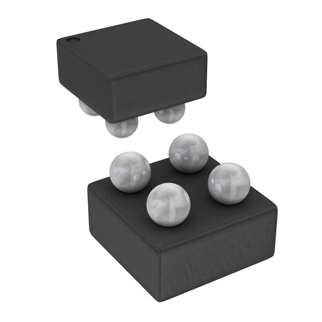
The M24128S-FCU is delivered in a 4-ball WLCSP package.
Figure 1. Logic diagram
9&&
6'$
6&/
0�����6�)&8
966
06�����9�
Table 1. Signal names
Signal name
Function
Direction
SDA
Serial Data
I/O
SCL
Serial Clock
Input
VCC
Supply voltage
VSS
Ground
Figure 2. 4-bump WLCSP connections
(top view, marking side, with balls on the underside)
9&&
6'$
t
;
966
<
6&/
06�����9�
6/30
DocID025717 Rev 3
�M24128S-FCU
Signal description
2
Signal description
2.1
Serial Clock (SCL)
SCL is an input. The signal applied on the SCL input is used to strobe the data available on
SDA(in) and to output the data on SDA(out).
2.2
Serial Data (SDA)
SDA is an input/output used to transfer data in or data out of the device. SDA(out) is an
open drain output that may be wire-OR’ed with other open drain or open collector signals on
the bus. A pull-up resistor must be connected from Serial Data (SDA) to VCC (Figure 9
indicates how to calculate the value of the pull-up resistor).
2.3
VSS (ground)
VSS is the reference for the VCC supply voltage.
2.4
Supply voltage (VCC)
2.4.1
Operating supply voltage (VCC)
Prior to selecting the memory and issuing instructions to it, a valid and stable VCC voltage
within the specified [VCC(min), VCC(max)] range must be applied (see Operating conditions
in Section 8: DC and AC parameters). In order to secure a stable DC supply voltage, it is
recommended to decouple the VCC line with a suitable capacitor (usually from10 nF to
100 nF) close to the VCC/VSS package pins.
This voltage must remain stable and valid until the end of the transmission of the instruction
and, for a write instruction, until the completion of the internal write cycle (tW).
2.4.2
Power-up conditions
The VCC voltage has to rise continuously from 0 V up to the minimum VCC operating voltage
(see Operating conditions in Section 8: DC and AC parameters) and the rise time must not
vary faster than 1 V/µs.
2.4.3
Device reset
In order to prevent inadvertent write operations during power-up, a power-on-reset (POR)
circuit is included.
At power-up, the device does not respond to any instruction until VCC has reached the
internal reset threshold voltage. This threshold is lower than the minimum VCC operating
voltage (see Operating conditions in Section 8: DC and AC parameters). When VCC passes
over the POR threshold, the device is reset and enters the Standby Power mode; however,
the device must not be accessed until VCC reaches a valid and stable DC voltage within the
specified [VCC(min), VCC(max)] range (see Operating conditions in Section 8: DC and AC
parameters).
DocID025717 Rev 3
7/30
29
�Signal description
M24128S-FCU
In a similar way, during power-down (continuous decrease in VCC), the device must not be
accessed when VCC drops below VCC(min). When VCC drops below the power-on-reset
threshold voltage, the device stops responding to any instruction sent to it.
2.4.4
Power-down conditions
During power-down (continuous decrease in VCC), the device must be in the Standby Power
mode (mode reached after decoding a Stop condition, assuming that there is no internal
write cycle in progress).
8/30
DocID025717 Rev 3
�M24128S-FCU
Memory organization
The memory is organized as shown below.
Figure 3. Block diagram
(IGHVOLTAGE
GENERATOR
#ONTROLLOGIC
3#,
3$!
)�/SHIFTREGISTER
!DDRESSREGISTER
ANDCOUNTER
$ATA
REGISTER
9DECODER
3
Memory organization
�PAGE
8DECODER
-3�����6�
DocID025717 Rev 3
9/30
29
�Device operation
4
M24128S-FCU
Device operation
The device supports the I2C protocol. This is summarized in Figure 4. Any device that sends
data on to the bus is defined to be a transmitter, and any device that reads the data to be a
receiver. The device that controls the data transfer is known as the bus master, and the
other as the slave device. A data transfer can only be initiated by the bus master, which will
also provide the serial clock for synchronization. The device is always a slave in all
communications.
Figure 4. I2C bus protocol
3#,
3$!
3$!
)NPUT
34!24
#ONDITION
3#,
�
3$!
-3"
�
3$!
#HANGE
34/0
#ONDITION
�
�
�
�
!#+
34!24
#ONDITION
3#,
�
3$!
-3"
�
�
�
�
�
!#+
34/0
#ONDITION
!)�����"
10/30
DocID025717 Rev 3
�M24128S-FCU
4.1
Device operation
Start condition
Start is identified by a falling edge of Serial Data (SDA) while Serial Clock (SCL) is stable in
the high state. A Start condition must precede any data transfer instruction. The device
continuously monitors (except during a Write cycle) Serial Data (SDA) and Serial Clock
(SCL) for a Start condition.
4.2
Stop condition
Stop is identified by a rising edge of Serial Data (SDA) while Serial Clock (SCL) is stable and
driven high. A Stop condition terminates communication between the device and the bus
master. A Read instruction that is followed by NoAck can be followed by a Stop condition to
force the device into the Standby mode.
A Stop condition at the end of a Write instruction triggers the internal Write cycle.
4.3
Data input
During data input, the device samples Serial Data (SDA) on the rising edge of Serial Clock
(SCL). For correct device operation, Serial Data (SDA) must be stable during the rising edge
of Serial Clock (SCL), and the Serial Data (SDA) signal must change only when Serial Clock
(SCL) is driven low.
4.4
Acknowledge bit (ACK)
The acknowledge bit is used to indicate a successful byte transfer. The bus transmitter,
whether it be bus master or slave device, releases Serial Data (SDA) after sending eight bits
of data. During the 9th clock pulse period, the receiver pulls Serial Data (SDA) low to
acknowledge the receipt of the eight data bits.
DocID025717 Rev 3
11/30
29
�Device operation
4.5
M24128S-FCU
Device addressing
To start communication between the bus master and the slave device, the bus master must
initiate a Start condition. Following this, the bus master sends the device select code, shown
in Table 2 (on Serial Data (SDA), most significant bit first).
Table 2. Device select code
Device type identifier(1)
Chip Enable address
RW
b7
b6
b5
b4
b3
b2
b1
b0
1
0
1
0
0
0
1
RW
1. The most significant bit, b7, is sent first.
The 8th bit is the Read/Write bit (RW). This bit is set to 1 for Read and 0 for Write operations.
If a match occurs on the device select code, the corresponding device gives an
acknowledgment on Serial Data (SDA) during the 9th bit time.
If the device does not match the device select code, the device deselects itself from the bus,
and goes into Standby mode (therefore will not acknowledge the device select code).
12/30
DocID025717 Rev 3
�M24128S-FCU
Instructions
5
Instructions
5.1
Write operations
Following a Start condition the bus master sends a device select code with the R/W bit (RW)
reset to 0. The device acknowledges this, as shown in Figure 5, and waits for two address
bytes. The device responds to each address byte with an acknowledge bit, and then waits
for the data byte.
Table 3. Most significant address byte
A15
A14
A13
A12
A11
A10
A9
A8
A1
A0
Table 4. Least significant address byte
A7
A6
A5
A4
A3
A2
When the bus master generates a Stop condition immediately after a data byte Ack bit (in
the “10th bit” time slot), either at the end of a Byte Write or a Page Write, the internal Write
cycle tW is triggered. A Stop condition at any other time slot does not trigger the internal
Write cycle.
After the Stop condition and the successful completion of an internal Write cycle (tW), the
device internal address counter is automatically incremented to point to the next byte after
the last modified byte.
During the internal Write cycle, Serial Data (SDA) is disabled internally, and the device does
not respond to any requests.
DocID025717 Rev 3
13/30
29
�Instructions
5.1.1
M24128S-FCU
Byte Write
After the device select code and the address bytes, the bus master sends one data byte. If
the addressed location is Write-protected, the device replies with NoAck, and the location is
not modified, as shown in Figure 6. If, instead, the addressed location is not Writeprotected, the device replies with Ack, as shown in Figure 5. The bus master shall terminate
the transfer by generating a Stop condition.
Figure 5. Write mode sequence (data write enabled)
!#+
$EVSEL
3TART
!#+
"YTEADDR
$ATAIN
!#+
"YTEADDR
!#+
$ATAIN�
$ATAIN�
2�7
!#+
$ATAIN.
3TOP
14/30
!#+
2�7
!#+
0AGE7RITE�CONTgD
"YTEADDR
"YTEADDR
!#+
0AGE7RITE
!#+
3TOP
$EVSEL
3TART
"YTE7RITE
!#+
DocID025717 Rev 3
!)�����E
�M24128S-FCU
Page Write
The Page Write mode allows up to 32 bytes to be written in a single Write cycle, provided
that they are all located in the same page in the memory: that is, the most significant
memory address bits, A15/A5, are the same. If more bytes are sent than will fit up to the end
of the page, a “roll-over” occurs, i.e. the bytes exceeding the page end are written on the
same page, from location 0.
The bus master sends from 1 to 32 bytes of data, each of which is acknowledged by the
device if the page is not write-protected, as shown in Figure 5. If the page is write-protected,
the contents of the addressed memory location are not modified, and each data byte is
followed by a NoAck, as shown in Figure 6. After each transferred byte, the internal page
address counter is incremented.
The transfer is terminated by the bus master generating a Stop condition.
Figure 6. Write mode sequence (data write inhibited)
ACK
ACK
Byte addr
Dev sel
Data in
ACK
Byte addr
ACK
Byte addr
NO ACK
Data in 1
Data in 2
R/W
NO ACK
NO ACK
Data in N
Stop
Page Write (cont'd)
Byte addr
NO ACK
R/W
ACK
Page Write
ACK
Stop
Dev sel
Start
Byte Write
Start
5.1.2
Instructions
DocID025717 Rev 3
AI01120e
15/30
29
�Instructions
5.1.3
M24128S-FCU
Write protection
By writing specific values in a register (Table 5) located at address 1xxx.xxxx.xxxx.xxxxb,
the memory array can be write-protected by blocks, which size can be defined as:
•
the upper quarter memory array
•
the upper half memory array
•
the upper 3/4 memory array
•
the whole memory array
Table 5. Write Protect register (Address = 1xxx.xxxx.xxxx.xxxxb)
b7
b6
b5
b4
Write
x
x
x
x
Read
0
0
0
0
Note:
b3
b2
b1
b0
Write protect
activation
Size of write
protected block
Size of write
protected
block
Write protect
lock
Location 1xxx.xxxx.xxxx.xxxxb is outside of the addressing field of the EEPROM memory
(16 Kbytes are addressed within the 00xx.xxxx.xxxx.xxxx range)
•
•
•
•
Bit b3 enables or disables the Write protection
–
b3=0: the whole memory can be written (no Write protection)
–
b3=1: the concerned block is write-protected
Bits b2 and b1 define the size of the memory block to be protected against write
instructions
–
b2,b1=0,0: the upper quarter of memory is write-protected
–
b2,b1=0,1: the upper half memory is write-protected
–
b2,b1=1,0: the upper 3/4 of memory are write-protected
–
b2,b1=1,1: the whole memory is write-protected
bit b0 locks the write protect status
–
b0=0: bits b3,b2,b1,b0 can be modified
–
b0=1: bits b3,b2,b1,b0 cannot be modified and therefore the memory write
protection is frozen.
b7, b6, b5, b4 bits are Don't Care bits.
Writing the Write Protect register
Writing in the Write protect register is performed with a Byte Write instruction at address
1xxx.xxxx.xxxx.xxxxb. Bits b7,b6,b5,b4 of the data byte are not significant (Don't Care).
Writing more than one byte will discard the write cycle (Write protect register content will not
be changed).
16/30
DocID025717 Rev 3
�M24128S-FCU
5.1.4
Instructions
Minimizing Write delays by polling on ACK
During the internal Write cycle, the device disconnects itself from the bus, and writes a copy
of the data from its internal latches to the memory cells. The maximum Write time (tw) is
shown in AC characteristics tables in Section 8: DC and AC parameters, but the typical time
is shorter. To make use of this, a polling sequence can be used by the bus master.
The sequence, as shown in Figure 7, is:
•
Initial condition: a Write cycle is in progress.
•
Step 1: the bus master issues a Start condition followed by a device select code (the
first byte of the new instruction).
•
Step 2: if the device is busy with the internal Write cycle, no Ack will be returned and
the bus master goes back to Step 1. If the device has terminated the internal Write
cycle, it responds with an Ack, indicating that the device is ready to receive the second
part of the instruction (the first byte of this instruction having been sent during Step 1).
Figure 7. Write cycle polling flowchart using ACK
tƌŝƚĞ�ĐLJĐůĞ
ŝŶ�ƉƌŽŐƌĞƐƐ��
^ƚĂƌƚ�ĐŽŶĚŝƚŝŽŶ
�ĞǀŝĐĞ�ƐĞůĞĐƚ
ǁŝƚŚ�Zt�с�Ϭ
EK
)LUVW�E\WH�RI�LQVWUXFWLRQ
ZLWK�5:� ���DOUHDG\
GHFRGHG�E\�WKH�GHYLFH
��<
ƌĞƚƵƌŶĞĚ
z�^
EK
EĞdžƚ
KƉĞƌĂƚŝŽŶ�ŝƐ
ĂĚĚƌĞƐƐŝŶŐ�ƚŚĞ
ŵĞŵŽƌLJ
z�^
^ĞŶĚ��ĚĚƌĞƐƐ
ĂŶĚ�ZĞĐĞŝǀĞ���<
ZĞ^ƚĂƌƚ
EK
^ƚŽƉ
�ĂƚĂ�ĨŽƌ�ƚŚĞ
tƌŝƚĞ�ĐƉĞƌĂƚŝŽŶ
�ŽŶƚŝŶƵĞ�ƚŚĞ
tƌŝƚĞ�ŽƉĞƌĂƚŝŽŶ
6WDUW&RQGLWLRQ
z�^
'HYLFH�VHOHFW
ZLWK�5:� ��
�ŽŶƚŝŶƵĞ�ƚŚĞ
ZĂŶĚŽŵ�ZĞĂĚ�ŽƉĞƌĂƚŝŽŶ
$,�����H
1. The seven most significant bits of the Device Select code of a Random Read (bottom right box in the
figure) must be identical to the seven most significant bits of the Device Select code of the Write (polling
instruction in the figure).
DocID025717 Rev 3
17/30
29
�Instructions
5.2
M24128S-FCU
Read operations
Read operations are performed independently of the Write protection state.
After the successful completion of a Read operation, the device internal address counter is
incremented by one, to point to the next byte address.
For the Read instructions, after each byte read (data out), the device waits for an
acknowledgment (data in) during the 9th bit time. If the bus master does not acknowledge
during this 9th time, the device terminates the data transfer and switches to its Standby
mode.
Figure 8. Read mode sequences
!#+
$ATAOUT
3TOP
3TART
$EVSEL
./!#+
2�7
!#+
2ANDOM
!DDRESS
2EAD
"YTEADDR
$EVSEL
!#+
!#+
$ATAOUT�
!#+
./!#+
$ATAOUT.
!#+
"YTEADDR
!#+
"YTEADDR
2�7
!#+
$EVSEL
3TART
$EVSEL
3TART
$ATAOUT
2�7
2�7
!#+
./!#+
3TOP
3TART
$EVSEL
3EQUENTION
2ANDOM
2EAD
!#+
"YTEADDR
2�7
!#+
3EQUENTIAL
#URRENT
2EAD
!#+
3TART
3TART
$EVSEL
!#+
3TOP
#URRENT
!DDRESS
2EAD
!#+
$ATAOUT�
2�7
./!#+
3TOP
$ATAOUT.
5.2.1
!)�����D
Random Address Read
A dummy Write is first performed to load the address into this address counter (as shown in
Figure 8) but without sending a Stop condition. Then, the bus master sends another Start
condition, and repeats the device select code, with the RW bit set to 1. The device
acknowledges this, and outputs the contents of the addressed byte. The bus master must
not acknowledge the byte, and terminates the transfer with a Stop condition.
18/30
DocID025717 Rev 3
�M24128S-FCU
5.2.2
Instructions
Current Address Read
For the Current Address Read operation, following a Start condition, the bus master only
sends a device select code with the R/W bit set to 1. The device acknowledges this, and
outputs the byte addressed by the internal address counter. The counter is then
incremented. The bus master terminates the transfer with a Stop condition, as shown in
Figure 8, without acknowledging the byte.
5.2.3
Sequential Read
This operation can be used after a Current Address Read or a Random Address Read. The
bus master does acknowledge the data byte output, and sends additional clock pulses so
that the device continues to output the next byte in sequence. To terminate the stream of
bytes, the bus master must not acknowledge the last byte, and must generate a Stop
condition, as shown in Figure 8.
The output data comes from consecutive addresses, with the internal address counter
automatically incremented after each byte output. After the last memory address, the
address counter “rolls-over”, and the device continues to output data from memory address
00h.
5.2.4
Read the Write Protect register
Reading the Write Protect register is performed with a Random Read instruction at address
1xxx.xxxx.xxxx.xxxxb. Bits b7, b6, b5, b4 of the Write Protect register content are read as
0, 0, 0, 0. The signification of the Protect Register lower bits b3, b2, b1, b0 are defined in
Section 5.1.3: Write protection.
Reading more than one byte will loop on reading the Write Protect Register value.
The Write Protect register cannot be read while a write cycle (tw) is ongoing.
DocID025717 Rev 3
19/30
29
�Initial delivery state
6
M24128S-FCU
Initial delivery state
The device is delivered with all the memory array bits set to 1 (each byte contains FFh) and
the Write Protect register set to 0 (00h).
20/30
DocID025717 Rev 3
�M24128S-FCU
7
Maximum rating
Maximum rating
Stressing the device outside the ratings listed in Table 6 may cause permanent damage to
the device. These are stress ratings only, and operation of the device at these, or any other
conditions outside those indicated in the operating sections of this specification, is not
implied. Exposure to absolute maximum rating conditions for extended periods may affect
device reliability.
Table 6. Absolute maximum ratings
Symbol
Parameter
Min.
Max.
Unit
Ambient operating temperature
–40
130
°C
TSTG
Storage temperature
–65
150
°C
TLEAD
Lead temperature during soldering
see
note(1)
-
°C
VIO
Input or output range
–0.50
6
V
IOL
DC output current (SDA = 0)
-
5
mA
VCC
Supply voltage
–0.50
6
V
VESD
Electrostatic pulse (Human Body model)
-
4000
V
1. Compliant with JEDEC standard J-STD-020D (for small-body, Sn-Pb or Pb assembly), the ST ECOPACK®
7191395 specification, and the European directive on Restrictions on Hazardous Substances (RoHS
directive 2011/65/EU of July 2011).
DocID025717 Rev 3
21/30
29
�DC and AC parameters
8
M24128S-FCU
DC and AC parameters
This section summarizes the operating and measurement conditions, and the DC and AC
characteristics of the device.
Table 7. Test conditions
Symbol
Parameter
Min.
Unit
Data retention(1)
TA = 55 °C
40
year
Cycling
TA = 25 °C
1 million
cycle
1. The data retention behavior is checked in production. The 40-year limit is defined from characterization and
qualification results.
Table 8. Operating conditions
Symbol
VCC
TA
fC
22/30
Parameter
Min.
Max.
Unit
V
Supply voltage
1.60
1.65
1.70
5.5
Ambient operating temperature: READ
–40
–40
–40
85
Ambient operating temperature: WRITE
0
–20
–40
85
Operating clock frequency
-
-
-
400
DocID025717 Rev 3
°C
kHz
�M24128S-FCU
DC and AC parameters
Table 9. DC characteristics
Symbol
Parameter
Test conditions
Min.
Max.
Unit
ILI
Input leakage current
(SCL, SDA)
VIN = VSS or VCC
device in Standby mode
-
±2
µA
ILO
Output leakage
current
SDA in Hi-Z, external voltage applied
on SDA: VSS or VCC
-
±2
µA
ICC
Supply current (Read) fc = 400 kHz
-
2
mA
ICC0
Supply current (Write) During tW
-
2
mA
Device not selected ,
VIN = VSS or VCC, VCC = 1.8 V
-
1
µA
Device not selected (1),
VIN = VSS or VCC, VCC = 2.5 V
-
2
µA
Device not selected (1),
VIN = VSS or VCC, VCC = 5.5 V
-
3
µA
(1)
ICC1
Standby supply
current
VIL
Input low voltage
(SCL, SDA)
-
–0.45
0.25 VCC
V
VIH
Input high voltage
(SCL, SDA)
-
0.75 VCC
VCC + 1
V
IOL = 1 mA, VCC