M24C01/02-W M24C01/02-R
M24C02-F
1-Kbit and 2-Kbit serial I²C bus EEPROMs
Datasheet - production data
Features
• Compatible with I2C bus modes:
– 400 kHz
– 100 kHz
TSSOP8 (DW)
169 mil width
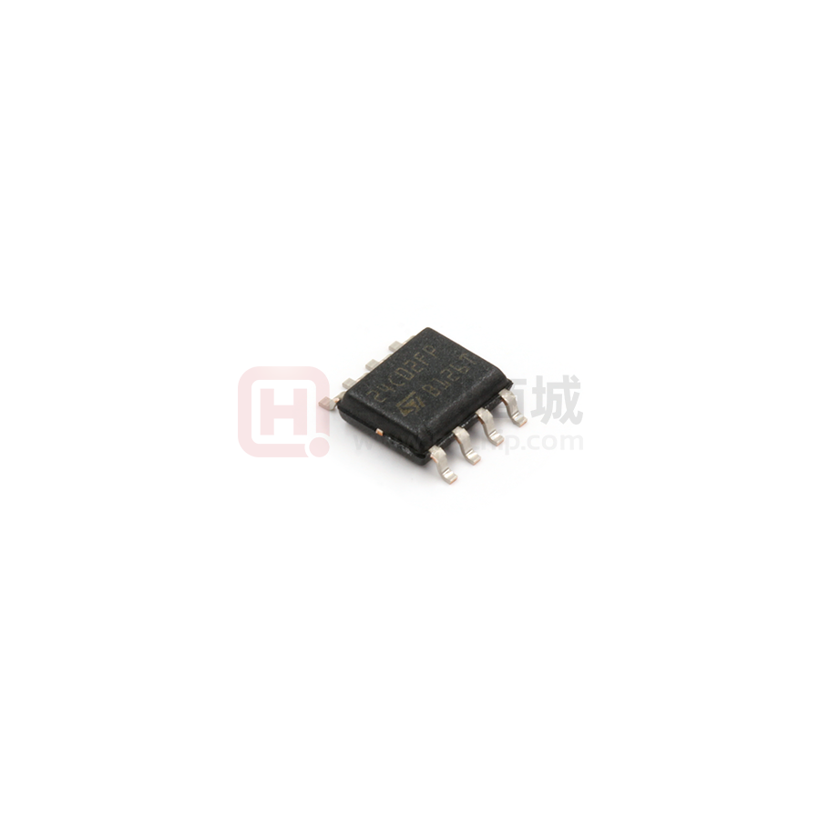
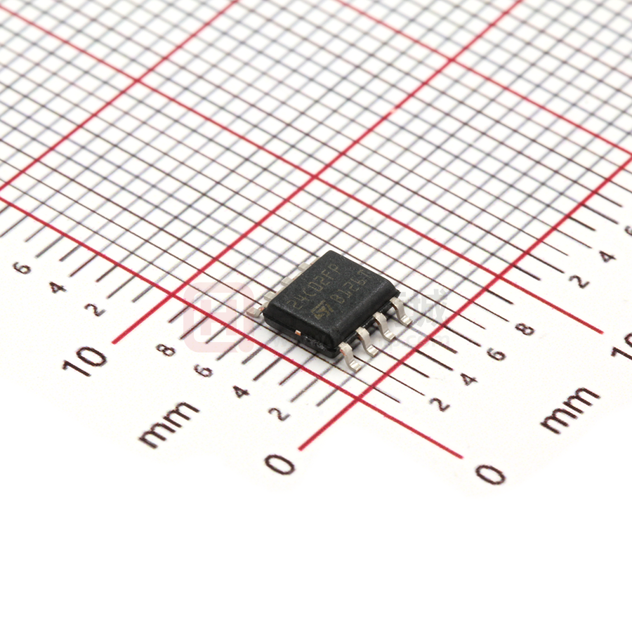
SO8 (MN)
150 mil width
�
�
PDIP8 (BN)(1)
• Memory array:
– 1 Kbit (128 bytes) of EEPROM
– 2 Kbit (256 bytes) of EEPROM
– Page size: 16 byte
• Single supply voltage:
– M24C01/02-W: 2.5 V to 5.5 V
– M24C01/02-R: 1.8 V to 5.5 V
– M24C02-F: 1.7 V to 5.5 V (full temperature
range) and 1.6 V to 1.7 V (limited
temperature range)
• Write:
– Byte Write within 5 ms
– Page Write within 5 ms
• Operating temperature range:
– from -40 °C up to +85 °C
• Random and sequential Read modes
• Write protect of the whole memory array
UFDFPN8 (MC)
DFN8 - 2 x 3 mm
• Enhanced ESD/Latch-Up protection
• More than 4 million Write cycles
• More than 200-years data retention
Packages
UFDFPN5 (MH)
DFN5 - 1.7 x 1.4 mm
• RoHS compliant and halogen-free
(ECOPACK2®)
1. Not recommended for new designs
October 2017
This is information on a product in full production.
DocID024020 Rev 6
1/42
www.st.com
�Contents
M24C01/02-W M24C01/02-R M24C02-F
Contents
1
Description . . . . . . . . . . . . . . . . . . . . . . . . . . . . . . . . . . . . . . . . . . . . . . . . . 6
2
Signal description . . . . . . . . . . . . . . . . . . . . . . . . . . . . . . . . . . . . . . . . . . . 8
2.1
Serial Clock (SCL) . . . . . . . . . . . . . . . . . . . . . . . . . . . . . . . . . . . . . . . . . . . 8
2.2
Serial Data (SDA) . . . . . . . . . . . . . . . . . . . . . . . . . . . . . . . . . . . . . . . . . . . . 8
2.3
Chip Enable (E2, E1, E0) . . . . . . . . . . . . . . . . . . . . . . . . . . . . . . . . . . . . . . 8
2.4
Write Control (WC) . . . . . . . . . . . . . . . . . . . . . . . . . . . . . . . . . . . . . . . . . . . 8
2.5
VSS (ground) . . . . . . . . . . . . . . . . . . . . . . . . . . . . . . . . . . . . . . . . . . . . . . . 8
2.6
Supply voltage (VCC) . . . . . . . . . . . . . . . . . . . . . . . . . . . . . . . . . . . . . . . . . 8
2.6.1
Operating supply voltage (VCC) . . . . . . . . . . . . . . . . . . . . . . . . . . . . . . . . 8
2.6.2
Power-up conditions . . . . . . . . . . . . . . . . . . . . . . . . . . . . . . . . . . . . . . . . 9
2.6.3
Device reset . . . . . . . . . . . . . . . . . . . . . . . . . . . . . . . . . . . . . . . . . . . . . . . 9
2.6.4
Power-down conditions . . . . . . . . . . . . . . . . . . . . . . . . . . . . . . . . . . . . . . 9
3
Memory organization . . . . . . . . . . . . . . . . . . . . . . . . . . . . . . . . . . . . . . . 10
4
Device operation . . . . . . . . . . . . . . . . . . . . . . . . . . . . . . . . . . . . . . . . . . . 11
5
4.1
Start condition . . . . . . . . . . . . . . . . . . . . . . . . . . . . . . . . . . . . . . . . . . . . . . 12
4.2
Stop condition . . . . . . . . . . . . . . . . . . . . . . . . . . . . . . . . . . . . . . . . . . . . . . 12
4.3
Data input . . . . . . . . . . . . . . . . . . . . . . . . . . . . . . . . . . . . . . . . . . . . . . . . . 12
4.4
Acknowledge bit (ACK) . . . . . . . . . . . . . . . . . . . . . . . . . . . . . . . . . . . . . . 12
4.5
Device addressing . . . . . . . . . . . . . . . . . . . . . . . . . . . . . . . . . . . . . . . . . . 13
Instructions . . . . . . . . . . . . . . . . . . . . . . . . . . . . . . . . . . . . . . . . . . . . . . . 14
5.1
5.2
2/42
Write operations . . . . . . . . . . . . . . . . . . . . . . . . . . . . . . . . . . . . . . . . . . . . 14
5.1.1
Byte Write . . . . . . . . . . . . . . . . . . . . . . . . . . . . . . . . . . . . . . . . . . . . . . . 15
5.1.2
Page Write . . . . . . . . . . . . . . . . . . . . . . . . . . . . . . . . . . . . . . . . . . . . . . . 16
5.1.3
Minimizing Write delays by polling on ACK . . . . . . . . . . . . . . . . . . . . . . 17
Read operations . . . . . . . . . . . . . . . . . . . . . . . . . . . . . . . . . . . . . . . . . . . . 18
5.2.1
Random Address Read . . . . . . . . . . . . . . . . . . . . . . . . . . . . . . . . . . . . . 19
5.2.2
Current Address Read . . . . . . . . . . . . . . . . . . . . . . . . . . . . . . . . . . . . . . 19
5.2.3
Sequential Read . . . . . . . . . . . . . . . . . . . . . . . . . . . . . . . . . . . . . . . . . . 19
DocID024020 Rev 6
�M24C01/02-W M24C01/02-R M24C02-F
Contents
6
Initial delivery state . . . . . . . . . . . . . . . . . . . . . . . . . . . . . . . . . . . . . . . . . 20
7
Maximum rating . . . . . . . . . . . . . . . . . . . . . . . . . . . . . . . . . . . . . . . . . . . . 21
8
DC and AC parameters . . . . . . . . . . . . . . . . . . . . . . . . . . . . . . . . . . . . . . 22
9
Package information . . . . . . . . . . . . . . . . . . . . . . . . . . . . . . . . . . . . . . . . 30
9.1
UFDFPN5 (DFN5) package information . . . . . . . . . . . . . . . . . . . . . . . . . . 30
9.2
TSSOP8 package information . . . . . . . . . . . . . . . . . . . . . . . . . . . . . . . . . 32
9.3
SO8N package information . . . . . . . . . . . . . . . . . . . . . . . . . . . . . . . . . . . 33
9.4
PDIP8 package information . . . . . . . . . . . . . . . . . . . . . . . . . . . . . . . . . . . 35
9.5
UFDFPN8 (DFN8) package information . . . . . . . . . . . . . . . . . . . . . . . . . . 36
10
Ordering information . . . . . . . . . . . . . . . . . . . . . . . . . . . . . . . . . . . . . . . 38
11
Revision history . . . . . . . . . . . . . . . . . . . . . . . . . . . . . . . . . . . . . . . . . . . 40
DocID024020 Rev 6
3/42
3
�List of tables
M24C01/02-W M24C01/02-R M24C02-F
List of tables
Table 1.
Table 2.
Table 3.
Table 4.
Table 5.
Table 6.
Table 7.
Table 8.
Table 9.
Table 10.
Table 11.
Table 12.
Table 13.
Table 14.
Table 15.
Table 16.
Table 17.
Table 18.
Table 19.
Table 20.
Table 21.
Table 22.
Table 23.
4/42
Signal names . . . . . . . . . . . . . . . . . . . . . . . . . . . . . . . . . . . . . . . . . . . . . . . . . . . . . . . . . . . . 6
Device select code . . . . . . . . . . . . . . . . . . . . . . . . . . . . . . . . . . . . . . . . . . . . . . . . . . . . . . . 13
Address byte . . . . . . . . . . . . . . . . . . . . . . . . . . . . . . . . . . . . . . . . . . . . . . . . . . . . . . . . . . . . 14
Absolute maximum ratings . . . . . . . . . . . . . . . . . . . . . . . . . . . . . . . . . . . . . . . . . . . . . . . . . 21
Operating conditions (voltage range W) . . . . . . . . . . . . . . . . . . . . . . . . . . . . . . . . . . . . . . . 22
Operating conditions (voltage range R) . . . . . . . . . . . . . . . . . . . . . . . . . . . . . . . . . . . . . . . 22
Operating conditions (voltage range F) . . . . . . . . . . . . . . . . . . . . . . . . . . . . . . . . . . . . . . . 22
AC measurement conditions. . . . . . . . . . . . . . . . . . . . . . . . . . . . . . . . . . . . . . . . . . . . . . . . 22
Input parameters. . . . . . . . . . . . . . . . . . . . . . . . . . . . . . . . . . . . . . . . . . . . . . . . . . . . . . . . . 23
Cycling performance . . . . . . . . . . . . . . . . . . . . . . . . . . . . . . . . . . . . . . . . . . . . . . . . . . . . . . 23
Memory cell data retention . . . . . . . . . . . . . . . . . . . . . . . . . . . . . . . . . . . . . . . . . . . . . . . . . 23
DC characteristics (M24C01/02-W, device grade 6). . . . . . . . . . . . . . . . . . . . . . . . . . . . . . 24
DC characteristics (M24C01/02-R device grade 6) . . . . . . . . . . . . . . . . . . . . . . . . . . . . . . 25
DC characteristics (M24C02-F, device grade 6). . . . . . . . . . . . . . . . . . . . . . . . . . . . . . . . . 26
400 kHz AC characteristics (I2C Fast-mode) . . . . . . . . . . . . . . . . . . . . . . . . . . . . . . . . . . . 27
100 kHz AC characteristics (I2C Standard mode). . . . . . . . . . . . . . . . . . . . . . . . . . . . . . . . 28
UFDFPN5 - 1.7 × 1.4 mm, 0.55 mm thickness, ultra thin fine pitch
dual flat package, no lead - package mechanical data . . . . . . . . . . . . . . . . . . . . . . . . . . . . 30
TSSOP8 – 3 x 4.4 mm, 0.65 mm pitch, 8-lead thin shrink small outline,
package mechanical data . . . . . . . . . . . . . . . . . . . . . . . . . . . . . . . . . . . . . . . . . . . . . . . . . . 32
SO8N – 3.9x4.9 mm, 8-lead plastic small outline, 150 mils body width,
package mechanical data . . . . . . . . . . . . . . . . . . . . . . . . . . . . . . . . . . . . . . . . . . . . . . . . . . 33
PDIP8 – 8-pin plastic DIP, 0.25 mm lead frame, package mechanical data. . . . . . . . . . . . 35
UFDFPN8 - 8-lead, 2 × 3 mm, 0.5 mm pitch ultra thin profile fine pitch dual
flat package mechanical data . . . . . . . . . . . . . . . . . . . . . . . . . . . . . . . . . . . . . . . . . . . . . . 36
Ordering information scheme . . . . . . . . . . . . . . . . . . . . . . . . . . . . . . . . . . . . . . . . . . . . . . . 38
Document revision history . . . . . . . . . . . . . . . . . . . . . . . . . . . . . . . . . . . . . . . . . . . . . . . . . 40
DocID024020 Rev 6
�M24C01/02-W M24C01/02-R M24C02-F
List of figures
List of figures
Figure 1.
Figure 2.
Figure 3.
Figure 4.
Figure 5.
Figure 6.
Figure 7.
Figure 8.
Figure 9.
Figure 10.
Figure 11.
Logic diagram . . . . . . . . . . . . . . . . . . . . . . . . . . . . . . . . . . . . . . . . . . . . . . . . . . . . . . . . . . . 6
8-pin package connections, top view . . . . . . . . . . . . . . . . . . . . . . . . . . . . . . . . . . . . . . . . . . 6
UFDFPN5 (DFN5) package connections . . . . . . . . . . . . . . . . . . . . . . . . . . . . . . . . . . . . . . . 7
Block diagram . . . . . . . . . . . . . . . . . . . . . . . . . . . . . . . . . . . . . . . . . . . . . . . . . . . . . . . . . . . 10
I2C bus protocol . . . . . . . . . . . . . . . . . . . . . . . . . . . . . . . . . . . . . . . . . . . . . . . . . . . . . . . . . 11
Write mode sequences with WC = 0 (data write enabled) . . . . . . . . . . . . . . . . . . . . . . . . . 15
Write mode sequences with WC = 1 (data write inhibited) . . . . . . . . . . . . . . . . . . . . . . . . . 16
Write cycle polling flowchart using ACK . . . . . . . . . . . . . . . . . . . . . . . . . . . . . . . . . . . . . . . 17
Read mode sequences . . . . . . . . . . . . . . . . . . . . . . . . . . . . . . . . . . . . . . . . . . . . . . . . . . . . 18
AC measurement I/O waveform . . . . . . . . . . . . . . . . . . . . . . . . . . . . . . . . . . . . . . . . . . . . . 22
Figure 12.
Figure 13.
AC waveforms . . . . . . . . . . . . . . . . . . . . . . . . . . . . . . . . . . . . . . . . . . . . . . . . . . . . . . . . . . 29
UFDFPN5 – 1.7x1.4 mm, 0.55 mm thickness, ultra thin fine pitch
dual flat package, no lead - package outline . . . . . . . . . . . . . . . . . . . . . . . . . . . . . . . . . . . 30
UFDFPN5 - 5-lead, 1.7 × 1.4 mm, 0.55 mm thickness, ultra thin fine pitch
dual flat package, no lead recommended footprint . . . . . . . . . . . . . . . . . . . . . . . . . . . . . . . 31
TSSOP8 – 3x4.4 mm, 0.65 mm pitch, 8-lead thin shrink small outline,
package outline. . . . . . . . . . . . . . . . . . . . . . . . . . . . . . . . . . . . . . . . . . . . . . . . . . . . . . . . . . 32
SO8N – 3.9x4.9 mm, 8-lead plastic small outline, 150 mils body width, package outline . 33
SO8N – 3.9x4.9 mm, 8-lead plastic small outline, 150 mils body width,
package recommended footprint . . . . . . . . . . . . . . . . . . . . . . . . . . . . . . . . . . . . . . . . . . . . 34
PDIP8 – 8-pin plastic DIP, 0.25 mm lead frame, package outline . . . . . . . . . . . . . . . . . . . 35
UFDFPN8 - 8-lead, 2 × 3 mm, 0.5 mm pitch ultra thin profile fine pitch dual
flat package outline . . . . . . . . . . . . . . . . . . . . . . . . . . . . . . . . . . . . . . . . . . . . . . . . . . . . . . 36
UFDFPN8 - 8-lead, 2 × 3 mm, 0.5 mm pitch ultra thin profile fine pitch dual
flat recommended footprint . . . . . . . . . . . . . . . . . . . . . . . . . . . . . . . . . . . . . . . . . . . . . . . . 37
Figure 14.
Figure 15.
Figure 16.
Figure 17.
Figure 18.
Figure 19.
Figure 20.
Maximum Rbus value versus bus parasitic capacitance (Cbus) for
an I2C bus at maximum frequency fC = 400 kHz . . . . . . . . . . . . . . . . . . . . . . . . . . . . . . . . . . . . 29
DocID024020 Rev 6
5/42
5
�Description
1
M24C01/02-W M24C01/02-R M24C02-F
Description
The M24C01(C02) is a 1(2)-Kbit I2C-compatible EEPROM (Electrically Erasable
PROgrammable Memory) organized as 128 (256) × 8 bits.
The M24C01/02-W can be accessed with a supply voltage from 2.5 V to 5.5 V, the
M24C01/02-R can be accessed with a supply voltage from 1.8 V to 5.5 V, and the
M24C02-F can be accessed either with a supply voltage from 1.7 V to 5.5 V (over the full
temperature range) or with an extended supply voltage from 1.6 V to 1.7 V if the
temperature is reduced to 0 °C/ 85 °C. All these devices operate with a maximum clock
frequency of 400 kHz.
Figure 1. Logic diagram
9&&
�
(��(�
6'$
0��[[[
6&/
:&
966
$,�����I
Table 1. Signal names
Signal name
(1)
Function
Direction
E2, E1, E0
Chip Enable
Input
SDA
Serial Data
I/O
SCL
Serial Clock
Input
WC
Write Control
Input
VCC
Supply voltage
-
VSS
Ground
-
1. Signal not connected in the DFN5 package.
Figure 2. 8-pin package connections, top view
(�
�
�
9&&
(�
�
�
:&
(�
�
�
6&/
966
�
�
6'$
$,�����I
6/42
DocID024020 Rev 6
�M24C01/02-W M24C01/02-R M24C02-F
Description
Figure 3. UFDFPN5 (DFN5) package connections
6 ## �
6 33 �
3$! �
!"#$
89:7
� 7#
�
� 6 33
� 3#,
�
�
�
�
�
4OPVIEW
�MARKINGSIDE
"OTTOMVIEW
�PADSSIDE
-3�����6�
1. Inputs E2, E1, E0 are not connected, therefore read as (000). Please refer to Section 2.3 for further
explanations.
DocID024020 Rev 6
7/42
41
�Signal description
M24C01/02-W M24C01/02-R M24C02-F
2
Signal description
2.1
Serial Clock (SCL)
The signal applied on the SCL input is used to strobe the data available on SDA(in) and to
output the data on SDA(out).
2.2
Serial Data (SDA)
SDA is an input/output used to transfer data in or data out of the device. SDA(out) is an
open drain output that may be wire-OR’ed with other open drain or open collector signals on
the bus. A pull-up resistor must be connected from Serial Data (SDA) to VCC (Figure 11
indicates how to calculate the value of the pull-up resistor).
2.3
Chip Enable (E2, E1, E0)
(E2,E1,E0) input signals are used to set the value that is to be looked for on the three least
significant bits (b3, b2, b1) of the 7-bit device select code. These inputs must be tied to VCC
or VSS, as shown in Table 2: Device select code. When not connected (left floating), these
inputs are read as low (0).
For the UFDFPN5 package, the (E2,E1,E0) inputs are not connected, therefore read as
(0,0,0).
2.4
Write Control (WC)
This input signal is useful for protecting the entire contents of the memory from inadvertent
write operations. Write operations are disabled to the entire memory array when Write
Control (WC) is driven high. Write operations are enabled when Write Control (WC) is either
driven low or left floating.
When Write Control (WC) is driven high, device select and address bytes are
acknowledged, Data bytes are not acknowledged.
2.5
VSS (ground)
VSS is the reference for the VCC supply voltage.
2.6
Supply voltage (VCC)
2.6.1
Operating supply voltage (VCC)
Prior to selecting the memory and issuing instructions to it, a valid and stable VCC voltage
within the specified [VCC(min), VCC(max)] range must be applied (see Operating conditions
in Section 8: DC and AC parameters). In order to secure a stable DC supply voltage, it is
recommended to decouple the VCC line with a suitable capacitor (usually of the order of
10 nF to 100 nF) close to the VCC/VSS package pins.
8/42
DocID024020 Rev 6
�M24C01/02-W M24C01/02-R M24C02-F
Signal description
This voltage must remain stable and valid until the end of the transmission of the instruction
and, for a write instruction, until the completion of the internal write cycle (tW).
2.6.2
Power-up conditions
The VCC voltage has to rise continuously from 0 V up to the minimum VCC operating voltage
(see Operating conditions in Section 8: DC and AC parameters).
2.6.3
Device reset
In order to prevent inadvertent write operations during power-up, a power-on-reset (POR)
circuit is included.
At power-up, the device does not respond to any instruction until VCC has reached the
internal reset threshold voltage. This threshold is lower than the minimum VCC operating
voltage (see Operating conditions in Section 8: DC and AC parameters). When VCC passes
over the POR threshold, the device is reset and enters the Standby Power mode; however,
the device must not be accessed until VCC reaches a valid and stable DC voltage within the
specified [VCC(min), VCC(max)] range (see Operating conditions in Section 8: DC and AC
parameters).
In a similar way, during power-down (continuous decrease in VCC), the device must not be
accessed when VCC drops below VCC(min). When VCC drops below the threshold voltage,
the device stops responding to any instruction sent to it.
2.6.4
Power-down conditions
During power-down (continuous decrease in VCC), the device must be in the Standby Power
mode (mode reached after decoding a Stop condition, assuming that there is no internal
write cycle in progress).
DocID024020 Rev 6
9/42
41
�Memory organization
3
M24C01/02-W M24C01/02-R M24C02-F
Memory organization
The memory is organized as shown below.
Figure 4. Block diagram
7#
%��%��%�
(IGHVOLTAGE
GENERATOR
#ONTROLLOGIC
3#,
3$!
)�/SHIFTREGISTER
$ATA
REGISTER
9DECODER
!DDRESSREGISTER
ANDCOUNTER
�PAGE
8DECODER
-3�����6�
10/42
DocID024020 Rev 6
�M24C01/02-W M24C01/02-R M24C02-F
4
Device operation
Device operation
The device supports the I2C protocol. This is summarized in Figure 5. Any device that sends
data on to the bus is defined to be a transmitter, and any device that reads the data to be a
receiver. The device that controls the data transfer is known as the bus master, and the
other as the slave device. A data transfer can only be initiated by the bus master, which will
also provide the serial clock for synchronization. The device is always a slave in all
communications.
Figure 5. I2C bus protocol
DocID024020 Rev 6
11/42
41
�Device operation
4.1
M24C01/02-W M24C01/02-R M24C02-F
Start condition
Start is identified by a falling edge of Serial Data (SDA) while Serial Clock (SCL) is stable in
the high state. A Start condition must precede any data transfer instruction. The device
continuously monitors (except during a Write cycle) Serial Data (SDA) and Serial Clock
(SCL) for a Start condition.
4.2
Stop condition
Stop is identified by a rising edge of Serial Data (SDA) while Serial Clock (SCL) is stable and
driven high. A Stop condition terminates communication between the device and the bus
master. A Read instruction that is followed by NoAck can be followed by a Stop condition to
force the device into the Standby mode.
A Stop condition at the end of a Write instruction triggers the internal Write cycle.
4.3
Data input
During data input, the device samples Serial Data (SDA) on the rising edge of Serial Clock
(SCL). For correct device operation, Serial Data (SDA) must be stable during the rising edge
of Serial Clock (SCL), and the Serial Data (SDA) signal must change only when Serial Clock
(SCL) is driven low.
4.4
Acknowledge bit (ACK)
The acknowledge bit is used to indicate a successful byte transfer. The bus transmitter,
whether it be bus master or slave device, releases Serial Data (SDA) after sending eight bits
of data. During the 9th clock pulse period, the receiver pulls Serial Data (SDA) low to
acknowledge the receipt of the eight data bits.
12/42
DocID024020 Rev 6
�M24C01/02-W M24C01/02-R M24C02-F
4.5
Device operation
Device addressing
To start communication between the bus master and the slave device, the bus master must
initiate a Start condition. Following this, the bus master sends the device select code, shown
in Table 2 (most significant bit first).
When using the DFN5 package, the Ei pins are not accessible. These inputs are read as low
(0).
As a result, to properly communicate with the device in DFN5 package, the E0, E1 and E2
bits must always be set to logic 0 for any operation. See Table 2.
Table 2. Device select code
Device type identifier(1)
Chip Enable address
R/W
Package
b7
b6
b5
b4
b3
b2
b1
b0
TSSOP8,SO8,PDIP8,
UFDFPN8
1
0
1
0
E2
E1
E0
R/W
DFN5
1
0
1
0
0
0
0
R/W
1. The MSB b7 is sent first.
The 8th bit is the Read/Write bit (RW). This bit is set to 1 for Read and 0 for Write operations.
If a match occurs on the device select code, the corresponding device gives an
acknowledgment on Serial Data (SDA) during the 9th bit time. If the device does not match
the device select code, it deselects itself from the bus, and goes into Standby mode.
DocID024020 Rev 6
13/42
41
�Instructions
M24C01/02-W M24C01/02-R M24C02-F
5
Instructions
5.1
Write operations
Following a Start condition the bus master sends a device select code with the R/W bit (RW)
reset to 0. The device acknowledges this, as shown in Figure 5, and waits for the address
byte. The device responds to each address byte with an acknowledge bit, and then waits for
the data byte.
Table 3. Address byte
A7
A6
A5
A4
A3
A2
A1
A0
When the bus master generates a Stop condition immediately after a data byte Ack bit (in
the “10th bit” time slot), either at the end of a Byte Write or a Page Write, the internal Write
cycle tW is triggered. A Stop condition at any other time slot does not trigger the internal
Write cycle.
After the Stop condition and the successful completion of an internal Write cycle (tW), the
device internal address counter is automatically incremented to point to the next byte after
the last modified byte.
During the internal Write cycle, Serial Data (SDA) is disabled internally, and the device does
not respond to any requests.
If the Write Control input (WC) is driven High, the Write instruction is not executed and the
accompanying data bytes are not acknowledged, as shown in Figure 6.
14/42
DocID024020 Rev 6
�M24C01/02-W M24C01/02-R M24C02-F
Byte Write
After the device select code and the address byte, the bus master sends one data byte. If
the addressed location is Write-protected, by Write Control (WC) being driven high, the
device replies with NoAck, and the location is not modified. If, instead, the addressed
location is not Write-protected, the device replies with Ack. The bus master terminates the
transfer by generating a Stop condition, as shown in Figure 5.
Figure 6. Write mode sequences with WC = 0 (data write enabled)
7#
!#+
!#+
"YTEADDRESS
!#+
$ATAIN
3TOP
$EV3ELECT
3TART
"YTE7RITE
2�7
7#
!#+
0AGE7RITE
$EV3ELECT
3TART
!#+
"YTEADDRESS
!#+
$ATAIN�
!#+
$ATAIN�
$ATAIN�
2�7
7#�CONTgD
!#+
0AGE7RITE
�CONTgD
!#+
$ATAIN.
3TOP
5.1.1
Instructions
DocID024020 Rev 6
!)�����C
15/42
41
�Instructions
5.1.2
M24C01/02-W M24C01/02-R M24C02-F
Page Write
The Page Write mode allows up to 16 byte to be written in a single Write cycle, provided that
they are all located in the same page in the memory: that is, the most significant memory
address bits, A8/A4, are the same. If more bytes are sent than will fit up to the end of the
page, a “roll-over” occurs, i.e. the bytes exceeding the page end are written on the same
page, from location 0.
The bus master sends from 1 to 16 byte of data, each of which is acknowledged by the
device if Write Control (WC) is low. If Write Control (WC) is high, the contents of the
addressed memory location are not modified, and each data byte is followed by a NoAck, as
shown in Figure 6. After each transferred byte, the internal page address counter is
incremented.
The transfer is terminated by the bus master generating a Stop condition.
Figure 7. Write mode sequences with WC = 1 (data write inhibited)
7#
!#+
"YTEADDRESS
./!#+
$ATAIN
3TOP
$EVSELECT
3TART
"YTE7RITE
!#+
2�7
7#
!#+
$EVSELECT
3TART
0AGE7RITE
!#+
"YTEADDRESS
./!#+
$ATAIN�
./!#+
$ATAIN�
$ATAIN�
2�7
7#�CONTgD
./!#+
$ATAIN.
3TOP
0AGE7RITE
�CONTgD
./!#+
!)�����D
16/42
DocID024020 Rev 6
�M24C01/02-W M24C01/02-R M24C02-F
5.1.3
Instructions
Minimizing Write delays by polling on ACK
The maximum Write time (tw) is shown in AC characteristics tables in Section 8: DC and AC
parameters, but the typical time is shorter. To make use of this, a polling sequence can be
used by the bus master.
The sequence, as shown in Figure 8, is:
•
Initial condition: a Write cycle is in progress.
•
Step 1: the bus master issues a Start condition followed by a device select code (the
first byte of the new instruction).
•
Step 2: if the device is busy with the internal Write cycle, no Ack will be returned and
the bus master goes back to Step 1. If the device has terminated the internal Write
cycle, it responds with an Ack, indicating that the device is ready to receive the second
part of the instruction (the first byte of this instruction having been sent during Step 1).
Figure 8. Write cycle polling flowchart using ACK
:ULWH�F\FOH
LQ�SURJUHVV��
6WDUW�FRQGLWLRQ
'HYLFH�VHOHFW
ZLWK�5:� ��
12
$&.
UHWXUQHG


 工商网监
湘ICP备2023018690号
工商网监
湘ICP备2023018690号
