M34E04
4-Kbit Serial Presence Detect (SPD) EEPROM compatible
with JEDEC EE1004
Datasheet - production data
Features
• 512-byte Serial Presence Detect EEPROM
compatible with JEDEC EE1004 specification
• Compatible with SMBus serial interface:
– up to 1 MHz transfer rate
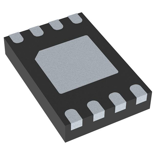
UFDFPN8 (MC)
2 x 3 mm
• EEPROM memory array:
– 4 Kbits organized as two pages of
256 bytes each
– Each page is composed of two 128-byte
blocks
• Software data protection for each 128-byte
block
• Write:
– Byte Write within 5 ms
– 16 bytes Page Write within 5 ms
• Noise filtering:
– Schmitt trigger on bus inputs
– Noise filter on bus inputs
• Single supply voltage:
– 1.7 V to 3.6 V
• Operating temperature range:
– from 0 °C up to +95 °C
• Enhanced ESD/latch-up protection
• More than 4million Write cycles
• More than 200-year data retention
• RoHS-compliant and halogen-free 8-lead ultra
thin fine pitch dual flat no lead package
(ECOPACK2®)
November 2014
This is information on a product in full production.
DocID023348 Rev 7
1/32
www.st.com
�Contents
M34E04
Contents
1
Description . . . . . . . . . . . . . . . . . . . . . . . . . . . . . . . . . . . . . . . . . . . . . . . . . 6
2
Signal description . . . . . . . . . . . . . . . . . . . . . . . . . . . . . . . . . . . . . . . . . . . 8
2.1
Serial clock (SCL) . . . . . . . . . . . . . . . . . . . . . . . . . . . . . . . . . . . . . . . . . . . . 8
2.2
Serial data (SDA) . . . . . . . . . . . . . . . . . . . . . . . . . . . . . . . . . . . . . . . . . . . . 8
2.3
Slave address (SA2, SA1, SA0) . . . . . . . . . . . . . . . . . . . . . . . . . . . . . . . . . 8
2.4
Write Control (WC) . . . . . . . . . . . . . . . . . . . . . . . . . . . . . . . . . . . . . . . . . . . 8
2.5
Supply voltage (VCC) . . . . . . . . . . . . . . . . . . . . . . . . . . . . . . . . . . . . . . . . . 9
2.5.1
3
2.5.3
Device reset . . . . . . . . . . . . . . . . . . . . . . . . . . . . . . . . . . . . . . . . . . . . . . . 9
2.5.4
Power-down conditions . . . . . . . . . . . . . . . . . . . . . . . . . . . . . . . . . . . . . . 9
Device operation . . . . . . . . . . . . . . . . . . . . . . . . . . . . . . . . . . . . . . . . . . . 11
3.1
Start condition . . . . . . . . . . . . . . . . . . . . . . . . . . . . . . . . . . . . . . . . . . . . . . .11
3.2
Stop condition . . . . . . . . . . . . . . . . . . . . . . . . . . . . . . . . . . . . . . . . . . . . . . .11
3.3
Acknowledge bit (ACK) . . . . . . . . . . . . . . . . . . . . . . . . . . . . . . . . . . . . . . .11
3.4
Data input . . . . . . . . . . . . . . . . . . . . . . . . . . . . . . . . . . . . . . . . . . . . . . . . . .11
3.5
Memory addressing . . . . . . . . . . . . . . . . . . . . . . . . . . . . . . . . . . . . . . . . . .11
3.6
Write operations . . . . . . . . . . . . . . . . . . . . . . . . . . . . . . . . . . . . . . . . . . . . 13
3.7
3.8
2/32
2.5.2
Operating supply voltage VCC . . . . . . . . . . . . . . . . . . . . . . . . . . . . . . . . . . . . . . . . . . 9
Power-up conditions . . . . . . . . . . . . . . . . . . . . . . . . . . . . . . . . . . . . . . . . 9
3.6.1
Byte write . . . . . . . . . . . . . . . . . . . . . . . . . . . . . . . . . . . . . . . . . . . . . . . . 13
3.6.2
Page write . . . . . . . . . . . . . . . . . . . . . . . . . . . . . . . . . . . . . . . . . . . . . . . 13
3.6.3
Minimizing system delays by polling on ACK . . . . . . . . . . . . . . . . . . . . 14
Read operations . . . . . . . . . . . . . . . . . . . . . . . . . . . . . . . . . . . . . . . . . . . . 15
3.7.1
Random address read . . . . . . . . . . . . . . . . . . . . . . . . . . . . . . . . . . . . . . 15
3.7.2
Current address read . . . . . . . . . . . . . . . . . . . . . . . . . . . . . . . . . . . . . . . 15
3.7.3
Sequential read . . . . . . . . . . . . . . . . . . . . . . . . . . . . . . . . . . . . . . . . . . . 16
3.7.4
Acknowledge in read mode . . . . . . . . . . . . . . . . . . . . . . . . . . . . . . . . . . 16
Setting the write protection . . . . . . . . . . . . . . . . . . . . . . . . . . . . . . . . . . . . 17
3.8.1
Set and clear the write protection (SWPn and CWP) . . . . . . . . . . . . . . 17
3.8.2
Read the protection status (RPSn) . . . . . . . . . . . . . . . . . . . . . . . . . . . . 18
3.8.3
Set the page address (SPAn) . . . . . . . . . . . . . . . . . . . . . . . . . . . . . . . . 18
3.8.4
Read the page address (RPA) . . . . . . . . . . . . . . . . . . . . . . . . . . . . . . . . 18
DocID023348 Rev 7
�M34E04
Contents
4
Initial delivery state . . . . . . . . . . . . . . . . . . . . . . . . . . . . . . . . . . . . . . . . . 19
5
Use within a DDR4 DRAM module . . . . . . . . . . . . . . . . . . . . . . . . . . . . . 19
5.1
Programming the M34E04 . . . . . . . . . . . . . . . . . . . . . . . . . . . . . . . . . . . . 19
5.1.1
Isolated DRAM module . . . . . . . . . . . . . . . . . . . . . . . . . . . . . . . . . . . . . 19
5.1.2
DRAM module inserted in the application motherboard . . . . . . . . . . . . 20
6
Maximum rating . . . . . . . . . . . . . . . . . . . . . . . . . . . . . . . . . . . . . . . . . . . . 22
7
DC and AC parameters . . . . . . . . . . . . . . . . . . . . . . . . . . . . . . . . . . . . . . 23
8
Package mechanical data . . . . . . . . . . . . . . . . . . . . . . . . . . . . . . . . . . . . 29
9
Part numbering . . . . . . . . . . . . . . . . . . . . . . . . . . . . . . . . . . . . . . . . . . . . 30
10
Revision history . . . . . . . . . . . . . . . . . . . . . . . . . . . . . . . . . . . . . . . . . . . 31
DocID023348 Rev 7
3/32
3
�List of tables
M34E04
List of tables
Table 1.
Table 2.
Table 3.
Table 4.
Table 5.
Table 6.
Table 7.
Table 8.
Table 9.
Table 10.
Table 11.
Table 12.
Table 13.
Table 14.
Table 15.
Table 16.
4/32
Signal names . . . . . . . . . . . . . . . . . . . . . . . . . . . . . . . . . . . . . . . . . . . . . . . . . . . . . . . . . . . . 7
Device Type Identifier Code (DTIC) . . . . . . . . . . . . . . . . . . . . . . . . . . . . . . . . . . . . . . . . . . 12
DRAM DIMM connections . . . . . . . . . . . . . . . . . . . . . . . . . . . . . . . . . . . . . . . . . . . . . . . . . 19
Acknowledge when writing data or defining the write-protection status (instructions
with R/W bit = 0) . . . . . . . . . . . . . . . . . . . . . . . . . . . . . . . . . . . . . . . . . . . . . . . . . . . . . . . . . 20
Acknowledge when reading the protection status (instructions with
R/W bit = 1). . . . . . . . . . . . . . . . . . . . . . . . . . . . . . . . . . . . . . . . . . . . . . . . . . . . . . . . . . . . . 20
Absolute maximum ratings . . . . . . . . . . . . . . . . . . . . . . . . . . . . . . . . . . . . . . . . . . . . . . . . . 22
Operating conditions (for temperature range 8 devices) . . . . . . . . . . . . . . . . . . . . . . . . . . 23
AC measurement conditions. . . . . . . . . . . . . . . . . . . . . . . . . . . . . . . . . . . . . . . . . . . . . . . . 23
Input parameters. . . . . . . . . . . . . . . . . . . . . . . . . . . . . . . . . . . . . . . . . . . . . . . . . . . . . . . . . 24
Cycling performance . . . . . . . . . . . . . . . . . . . . . . . . . . . . . . . . . . . . . . . . . . . . . . . . . . . . . . 24
Memory cell data retention . . . . . . . . . . . . . . . . . . . . . . . . . . . . . . . . . . . . . . . . . . . . . . . . . 24
DC characteristics. . . . . . . . . . . . . . . . . . . . . . . . . . . . . . . . . . . . . . . . . . . . . . . . . . . . . . . . 25
AC characteristics . . . . . . . . . . . . . . . . . . . . . . . . . . . . . . . . . . . . . . . . . . . . . . . . . . . . . . . . 26
UFDFPN8 (MLP8) 8-lead ultra thin fine pitch dual flat package no lead
2 x 3 mm, data29
Ordering information scheme . . . . . . . . . . . . . . . . . . . . . . . . . . . . . . . . . . . . . . . . . . . . . . . 30
Document revision history . . . . . . . . . . . . . . . . . . . . . . . . . . . . . . . . . . . . . . . . . . . . . . . . . 31
DocID023348 Rev 7
�M34E04
List of figures
List of figures
Figure 1.
Figure 2.
Figure 3.
Figure 4.
Figure 5.
Figure 6.
Figure 7.
Figure 8.
Figure 9.
Figure 10.
Figure 11.
Figure 12.
Figure 13.
Figure 14.
Logic diagram . . . . . . . . . . . . . . . . . . . . . . . . . . . . . . . . . . . . . . . . . . . . . . . . . . . . . . . . . . . . 6
8-pin package connections (top view) . . . . . . . . . . . . . . . . . . . . . . . . . . . . . . . . . . . . . . . . . 6
Device select code . . . . . . . . . . . . . . . . . . . . . . . . . . . . . . . . . . . . . . . . . . . . . . . . . . . . . . . . 8
Bus protocol . . . . . . . . . . . . . . . . . . . . . . . . . . . . . . . . . . . . . . . . . . . . . . . . . . . . . . . . . . . . 10
Write mode sequences in a non write-protected area . . . . . . . . . . . . . . . . . . . . . . . . . . . . 13
Write cycle polling flowchart using ACK . . . . . . . . . . . . . . . . . . . . . . . . . . . . . . . . . . . . . . . 14
Read mode sequences . . . . . . . . . . . . . . . . . . . . . . . . . . . . . . . . . . . . . . . . . . . . . . . . . . . . 16
Setting the write protection . . . . . . . . . . . . . . . . . . . . . . . . . . . . . . . . . . . . . . . . . . . . . . . . . 17
Serial presence detect block diagram. . . . . . . . . . . . . . . . . . . . . . . . . . . . . . . . . . . . . . . . . 21
AC measurement I/O waveform . . . . . . . . . . . . . . . . . . . . . . . . . . . . . . . . . . . . . . . . . . . . . 23
AC waveforms . . . . . . . . . . . . . . . . . . . . . . . . . . . . . . . . . . . . . . . . . . . . . . . . . . . . . . . . . . 27
Maximum Rbus value versus bus parasitic capacitance (Cbus) for an I2C bus at
maximum frequency fC = 1 MHz . . . . . . . . . . . . . . . . . . . . . . . . . . . . . . . . . . . . . . . . . . . . . 28
Maximum Rbus value versus bus parasitic capacitance (Cbus) for an I2C bus at
maximum frequency fc = 400 kHz. . . . . . . . . . . . . . . . . . . . . . . . . . . . . . . . . . . . . . . . . . . . 28
UFDFPN8 (MLP8) 8-lead ultra thin fine pitch dual flat no lead,
package outline. . . . . . . . . . . . . . . . . . . . . . . . . . . . . . . . . . . . . . . . . . . . . . . . . . . . . . . . . . 29
DocID023348 Rev 7
5/32
5
�Description
1
M34E04
Description
The M34E04 is a 512-byte EEPROM device designed to operate the SMBus bus in the
1.7 V - 3.6 V voltage range, with a maximum of 1 MHz transfer rate in the 2.2 V - 3.6 V
voltage range, over the JEDEC defined ambient temperature of 0°C / 95°C.
The M34E04 includes a 4-Kbit serial EEPROM organized as two pages of 256 bytes each,
or 512 bytes of total memory. Each page is composed of two 128-byte blocks. The device is
able to selectively lock the data in any or all of the four 128-byte blocks. Designed
specifically for use in DRAM DIMMs (Dual Inline Memory Modules) with Serial Presence
Detect, all the information concerning the DRAM module configuration (such as its access
speed, its size, its organization) can be kept write-protected in one or more memory blocks.
The M34E04 device is protocol-compatible with the previous generation of 2-Kbit devices,
M34E02. The page selection method allows commands used with legacy devices such as
M34E02 to be applied to the lower or upper pages of the EEPROM.
Individually locking a 128-byte block may be accomplished using a software write protection
mechanism in conjunction with a high input voltage VHV on input SA0. By sending the
device a specific SMBus sequence, each block may be protected from writes until the write
protection is electrically reversed using a separate SMBus sequence which also requires
VHV on input SA0. The write protection for all four blocks is cleared simultaneously.
Figure 1. Logic diagram
6##
�
3!��3!��3!�
3$!
-��%��
3#,
7#
633
!)�����C
Figure 2. 8-pin package connections (top view)
-��%��
3!�
3!�
3!�
633
�
�
�
�
�
�
�
�
6##
7#
3#,
3$!
!)�����C
1. See the Package mechanical data section for package dimensions, and how to identify pin 1.
6/32
DocID023348 Rev 7
�M34E04
Description
Table 1. Signal names
Signal names
Description
SA2, SA1, SA0
Slave address
SDA
Serial data
SCL
Serial clock
WC
Write control
VCC
Supply voltage
VSS
Ground
DocID023348 Rev 7
7/32
31
�Signal description
M34E04
2
Signal description
2.1
Serial clock (SCL)
The signal applied on this input is used to strobe the data available on SDA(in) and to output
the data on SDA(out).
If SCL is driven low for tTIMEOUT (see Table 13) or longer, the M34E04 is set back in
Standby mode, ready to receive a new START condition.
2.2
Serial data (SDA)
SDA is an input/output used to transfer data in or out of the device. SDA(out) is an open
drain output that may be wire-OR’ed with other open drain or open collector signals on the
bus. A pull-up resistor must be connected from Serial Data (SDA) to VCC. (Figure 12
indicates how the value of the pull-up resistor can be calculated).
2.3
Slave address (SA2, SA1, SA0)
(SA2,SA1,SA0) input signals are used to set the value that is to be looked for on the three
least significant bits (b3, b2, b1) of the 7-bit Device Type Identifier Code (DTIC, see
Table 2). These inputs must be tied to VCC or VSS, as shown in Figure 3. When not
connected (left floating), these inputs are read as low (0).
The SA0 input is used to detect the VHV voltage, when decoding an SWP or CWP
instruction.
Figure 3. Device select code
6##
6##
-��%��
-��%��
3! I
633
3! I
633
!I�����C
2.4
Write Control (WC)
This input signal is provided for protecting the contents of the whole memory from
inadvertent write operations. Write Control (WC) is used to enable (when driven low) or
disable (when driven high) write instructions to the entire memory area.
When Write Control (WC) is tied low or left unconnected, the write protection of the memory
is determined by the status defined by the execution of the previous SWPi instructions.
8/32
DocID023348 Rev 7
�M34E04
Signal description
2.5
Supply voltage (VCC)
2.5.1
Operating supply voltage VCC
Prior to selecting the memory and issuing instructions to it, a valid and stable VCC voltage
within the specified [VCC(min), VCC(max)] range must be applied (see Table 8). In order to
secure a stable DC supply voltage, it is recommended to decouple the VCC line with a
suitable capacitor (usually of the order of 10 nF to 100 nF) close to the VCC/VSS package
pins.
This voltage must remain stable and valid until the end of the transmission of the instruction
and, for a Write instruction, until the completion of the internal write cycle (tW).
2.5.2
Power-up conditions
The VCC voltage has to rise continuously from 0 V up to the minimum VCC operating voltage
defined in Table 8 and the rise time must not vary faster than 1 V/µs.
2.5.3
Device reset
In order to prevent inadvertent write operations during power-up, a power-on reset (POR)
circuit is included. At power-up, the device does not respond to any instruction until VCC
reaches the internal reset threshold voltage (this threshold is lower than the minimum VCC
operating voltage defined in Table 8).
When VCC passes over the POR threshold, the device is reset and enters the Standby
Power mode. However, the device must not be accessed until VCC reaches a valid and
stable VCC voltage within the specified [VCC(min), VCC(max)] range.
In a similar way, during power-down (continuous decrease in VCC), as soon as VCC drops
below the power-on reset threshold voltage, the device stops responding to any instruction
sent to it.
2.5.4
Power-down conditions
During power-down (continuous decrease in VCC), the device must be in Standby Power
mode (mode reached after decoding a Stop condition, assuming that there is no internal
write cycle in progress).
DocID023348 Rev 7
9/32
31
�Signal description
M34E04
Figure 4. Bus protocol
3#,
3$!
3$!
)NPUT
3TART
CONDITION
3#,
�
3$!
-3"
�
3$!
#HANGE
3TOP
CONDITION
�
�
�
�
!#+
3TART
CONDITION
3#,
�
3$!
-3"
�
�
�
�
�
!#+
3TOP
CONDITION
!)�����C
10/32
DocID023348 Rev 7
�M34E04
3
Device operation
Device operation
The device supports the I2C protocol. This is summarized in Figure 4. Any device that sends
data onto the bus is defined to be a transmitter, and any device that reads the data is
defined to be a receiver. The device that controls the data transfer is known as the bus
master, and the other device is known as the slave device. A data transfer can only be
initiated by the bus master, which will also provide the serial clock for synchronization. The
memory device is always a slave in all communication.
3.1
Start condition
Start is identified by a falling edge of Serial Data (SDA) while Serial Clock (SCL) is stable in
the high state. A Start condition must precede any data transfer command. The device
continuously monitors (except during a Write cycle) Serial Data (SDA) and Serial Clock
(SCL) for a Start condition.
3.2
Stop condition
Stop is identified by a rising edge of Serial Data (SDA) while Serial Clock (SCL) is stable and
driven high. A Stop condition terminates communication between the device and the bus
master. A Read command that is followed by NoAck can be followed by a Stop condition to
force the device into the Standby mode. A Stop condition at the end of a Write command
triggers the internal EEPROM Write cycle.
3.3
Acknowledge bit (ACK)
The acknowledge bit is used to indicate a successful byte transfer. The bus transmitter,
whether a bus master or a slave device, releases Serial Data (SDA) after sending eight bits
of data. During the 9th clock pulse period, the receiver pulls Serial Data (SDA) low to
acknowledge the receipt of the eight data bits.
3.4
Data input
During data input, the device samples Serial Data (SDA) on the rising edge of Serial Clock
(SCL). For correct device operation, Serial Data (SDA) must be stable during the rising edge
of Serial Clock (SCL), and the Serial Data (SDA) signal must change only when Serial Clock
(SCL) is driven low.
3.5
Memory addressing
To start a communication between the bus master and the slave device, the bus master
must initiate a Start condition. Following this, the bus master sends the device select code,
shown in Table 2 (on Serial Data (SDA), most significant bit first).
The Device Type Identifier Code (DTIC) consists of a 4-bit device type identifier, and a 3-bit
slave address (SA2, SA1, SA0). To address the memory array, the 4-bit device type
identifier is 1010b; to access the write-protection settings, it is 0110b.
DocID023348 Rev 7
11/32
31
�Device operation
M34E04
Table 2. Device Type Identifier Code (DTIC)
Device type identifier
(1)
Abbr
Select address
(2) (3)
R_W_n
SA0 pin
(4)
b7
b6
b5
b4
1
0
1
0
b3
b2
b1
b0
Read
RSPD
Write
WSPD
Set Write Protection, block 0
SWP0
0
0
1
0
VHV
Set Write Protection, block 1
SWP1
1
0
0
0
VHV
Set Write Protection, block 2
SWP2
1
0
1
0
VHV
Set Write Protection, block 3
SWP3
0
0
0
0
VHV
Clear All Write Protection
CWP
0
1
1
0
VHV
Read Protection Status, block 0 (5)
RPS0
0
0
1
1
0, 1 or VHV
Read Protection Status, block 1
(5)
RPS1
1
0
0
1
0, 1 or VHV
Read Protection Status, block 2
(5)
RPS2
1
0
1
1
0, 1 or VHV
Read Protection Status, block 3
(5)
RPS3
0
0
0
1
0, 1 or VHV
Set Page Address to 0 (6)
SPA0
1
1
0
0
0, 1 or VHV
(6)
SPA1
1
1
1
0
0, 1 or VHV
RPA
1
1
0
1
0, 1 or VHV
Set Page Address to 1
Read Page Address
(7)
Reserved
0
1
1
0
LSA2 LSA1 LSA0
-
1
0
0 or 1
All other encodings
1. The most significant bit, b7, is sent first.
2. Logical Serial Addresses (LSA) are generated by the combination of inputs on the SA pins.
3. For backward compatibility with M34E02 devices, the order of block select bits (b3 and b1) is not a simple binary encoding
of the block number.
4. SA0 pin is driven to Vss, Vcc or VHV.
5. Reading the block protection status results in Ack when the block is not write-protected, and results in NoAck when the
block is write-protected.
6. Setting the EE page address to 0 selects the lower 256 bytes of EEPROM; setting it to 1 selects the upper 256 bytes of
EEPROM. Subsequent Read EE or Write EE commands operate on the selected EE page.
7. Reading the EE page address results in Ack when the current page is 0, and NoAck when the current page is 1.
Up to eight memory devices can be connected on a single serial bus. Each one is given a
unique 3-bit code on the slave address (SA2, SA1, SA0) inputs. When the device select
code is received, the device only responds if the slave address is the same as the value on
the slave address (SA2, SA1, SA0) inputs.
The 8th bit is the Read/Write bit (RW). This bit is set to 1 for Read and 0 for Write operations.
If a match occurs on the device select code, the corresponding device gives an
acknowledgment on Serial Data (SDA) during the 9th bit time. If the device does not match
the device select code, it deselects itself from the bus, and goes into Standby mode.
12/32
DocID023348 Rev 7
�M34E04
3.6
Device operation
Write operations
Following a Start condition, the bus master sends a device select code with the RW bit reset
to 0. The device acknowledges this, as shown in Figure 5, and waits for an address byte.
The device responds to the address byte with an acknowledge bit, and then waits for the
data byte.
When the bus master generates a Stop condition immediately after a data byte Ack bit (in
the “10th bit” time slot), either at the end of a Byte write or a Page write, the internal memory
Write cycle is triggered. A Stop condition at any other time slot does not trigger the internal
Write cycle.
During the internal Write cycle, Serial Data (SDA) and Serial Clock (SCL) are ignored, and
the device does not respond to any requests.
3.6.1
Byte write
After the device select code and the address byte, the bus master sends one data byte. If
the addressed location is hardware write-protected, the device replies to the data byte with
NoAck, and the location is not modified. If, instead, the addressed location is not writeprotected, the device replies with Ack. The bus master terminates the transfer by generating
a Stop condition, as shown in Figure 5.
Figure 5. Write mode sequences in a non write-protected area
!#+
"YTEADDRESS
$ATAIN
2�7
!#+
$EVICESELECT
3TART
0AGE7RITE
!#+
3TOP
$EVICESELECT
3TART
"YTE7RITE
!#+
!#+
"YTEADDRESS
!#+
$ATAIN�
$ATAIN�
2�7
!#+
!#+
3TOP
$ATAIN.
3.6.2
!)�����B
Page write
The Page write mode allows up to 16 bytes to be written in a single Write cycle, provided
that they are all located in the same page in the memory: that is, the most significant
memory address bits are the same. If more bytes are sent than will fit up to the end of the
page, a condition known as ‘roll-over’ occurs. This should be avoided, as data starts to
become overwritten in an implementation dependent way.
The bus master sends from 1 to 16 bytes of data, each of which is acknowledged by the
device if Write Control (WC) is low. If the addressed location is hardware write-protected,
the device replies to the data byte with NoAck, and the locations are not modified. After
each byte is transferred, the internal byte address counter (the 4 least significant address
DocID023348 Rev 7
13/32
31
�Device operation
M34E04
bits only) is incremented. The transfer is terminated by the bus master generating a Stop
condition.
3.6.3
Minimizing system delays by polling on ACK
The sequence, as shown in Figure 6, is:
•
Initial condition: a Write cycle is in progress.
•
Step 1: the bus master issues a Start condition followed by a device select code (the
first byte of the new instruction).
•
Step 2: if the device is busy with the internal Write cycle, no Ack will be returned and
the bus master goes back to Step 1. If the device has terminated the internal Write
cycle, it responds with an Ack, indicating that the device is ready to receive the second
part of the instruction (the first byte of this instruction having been sent during Step 1).
Figure 6. Write cycle polling flowchart using ACK
:ULWH�F\FOH
LQ�SURJUHVV��
6WDUW�FRQGLWLRQ
'HYLFH�VHOHFW
ZLWK�5:� ��
12
$&.
UHWXUQHG
0.7VCC
500
-
kΩ
-
-
100
ns
tNS
Pulse width ignored (input filter on SCL and SDA)
1. Characterized, not tested in production.
Table 10. Cycling performance
Symbol
Parameter
Ncycle
Write cycle
endurance
Test condition
Max.
TA ≤ 25 °C, VCC(min) < VCC < VCC(max)
4,000,000
TA = 85 °C, VCC(min) < VCC < VCC(max)
1,200,000
Unit
Write cycle
Table 11. Memory cell data retention
Parameter
Data retention
(1)
Test condition
TA = 55 °C
Min.
Unit
200
Year
1. The data retention behavior is checked in production, while the 200-year limit is defined from
characterization and qualification results.
24/32
DocID023348 Rev 7
�M34E04
DC and AC parameters
Table 12. DC characteristics
Symbol
Parameter
Test condition (in addition to
those in Table 7)
Min
Max
Unit
ILI
Input leakage current (SCL,
SDA, SA0, SA1, SA2)
VIN = VSS or VCC
-
±2
µA
ILO
Output leakage current
SDA in Hi-Z, external voltage
applied on SDA: VSS or VCC
-
±2
µA
ICC
Supply current (read)
fc = 400 kHz or 1 MHz
-
1
mA
-
(1)
mA
ICC0
Supply current (write)
During tW, VIN = VSS or VCC
(2)
ICC1
Standby supply current
1
Device not selected ,
VIN = VSS or VCC, VCC ≥ 2.2 V
-
2
µA
Device not selected (2),
VIN = VSS or VCC, VCC < 2.2 V
-
1
µA
VIL
Input low voltage
(SCL, SDA, WC)
-
-0.45
0.3 VCC
V
VIH
Input high voltage
(SCL, SDA, WC)
-
0.7VCC
VCC+1
V
VCC < 2.2 V
7
10
V
VCC ≥ 2.2 V
VCC
+4.8 V
10
V
IOL = 20 mA, VCC ≥ 2.2 V
-
0.4
V
IOL = 6 mA, VCC ≤ 2 V
-
0.6
V
IOL = 3 mA, VCC ≤2 V
-
0.4
V
VHV
VOL
VPOR
VPDR
SA0 high voltage detect
Output low voltage
Power on reset threshold
Power down reset threshold
-
0.7
1.4
(1)
(1)
V
-
V
1. Measured during characterization, not tested in production.
2. The device is not selected after a power-up, after a read command (after the Stop condition), or after the
completion of the internal write cycle tW (tW is triggered by the correct decoding of a write command).
DocID023348 Rev 7
25/32
31
�DC and AC parameters
M34E04
Table 13. AC characteristics
VCC ≥ 2.2 V
VCC < 2.2 V
Symbol
100 kHz
Parameter
400 kHz
1000 kHz
Unit
Min.
Max.
Min.
Max.
Min.
Max.
10
100
10
400
10
1000
kHz
fSCL
fC
tHIGH
tCHCL
Clock pulse width high time
4000
-
600
-
260
-
ns
tCLCH
Clock pulse width low time
4700
-
1300
-
500
-
ns
(2)
Detect clock low timeout
25
35
25
35
25
35
ms
tLOW
(1)
tTIMEOUT
Clock frequency
(3)
tXH1XH2
SDA rise time
-
1000
20
300
-
120
ns
tF (3)
tQL1QL2
SDA(out) fall time
-
300
20
300
-
120
ns
tSU:DAT
tDXCH
Data in setup time
250
-
100
-
50
-
ns
tHD:DI
tCLDX
Data in hold time
0
-
0
-
0
-
ns
tHD:DAT
tCLQX
Data out hold time
200
3450
200
900
0
350
ns
tSU:STA (4)
tCHDL
Start condition setup time
4700
-
600
-
260
-
ns
tHD:STA
tDLCL
Stop condition hold time
4000
-
600
-
260
-
ns
tSU:STO
tCHDH
Stop condition setup time
4000
-
600
-
260
-
ns
tBUF
tDHDL
Time between Stop Condition and
next Start Condition
4700
-
1300
-
500
-
ns
-
5
-
5
-
5
ms
100
-
100
-
100
-
µs
0
-
0
-
0
-
µs
tR
tW
tPOFF (3)
tINIT (3)
Write time
Time ensuring a Reset when VCC
drops below VPDR(min)
Time from VCC(min) to the first
command
1. Initiate clock stretching, which is an optional SMBus bus feature.
2. A timeout condition can only be ensured if SCL is driven low for tTIMEOUT(Max) or longer; then the M34E04 is set in
Standby mode and is ready to receive a new START condition. If SCL is driven low for less than tTIMEOUT(Min), the M34E04
internal state remains unchanged.
3. Measured during characterization, not tested in production.
4. To avoid spurious START and STOP conditions, a minimum delay is placed between the falling edge of SCL and the falling
or rising edge of SDA.
26/32
DocID023348 Rev 7
�M34E04
DC and AC parameters
Figure 11. AC waveforms
6WDUW
FRQGLWLRQ
6WDUW
6WRS
FRQGLWLRQ FRQGLWLRQ
W;/�;/�
W;+�;+�
W&+&/
W&/&+
6&/
W'/&/
W;/�;/�
6'$�,Q
W&+'/
W;+�;+�
6'$
,QSXW
6'$ W';&+
&KDQJH
W&/';
W&+'+
6WRS
FRQGLWLRQ
W'+'/
6WDUW
FRQGLWLRQ
6&/
6'$�,Q
W:
W&+'+
W&+'/
:ULWH�F\FOH
W&+&/
6&/
W&/49
6'$�2XW
W&/4;
'DWD�YDOLG
W4/�4/�
'DWD�YDOLG
$,�����M
DocID023348 Rev 7
27/32
31
�DC and AC parameters
M34E04
"USLINEPULL
UPRESISTOR LȰ
Figure 12. Maximum Rbus value versus bus parasitic capacitance (Cbus) for an I2C bus at
maximum frequency fC = 1 MHz
���
6##
4HE2BUS§#BUSTIMECONSTANT
MUSTBEBELOWTHE���NS
TIMECONSTANTLINEREPRESENTED
ONTHELEFT�
2
BUS §
#
BUS �
��
��
�NS
�
2BUS
)£#BUS
MASTER
(ERE�
2 BUS § #BUS����NS
3#,
-��&XXX
3$!
#BUS
�
��
��
���
"USLINECAPACITOR�P&
-3�����6�
Figure 13. Maximum Rbus value versus bus parasitic capacitance (Cbus) for an I2C bus at
maximum frequency fc = 400 kHz
DL�����G
28/32
DocID023348 Rev 7
�M34E04
8
Package mechanical data
Package mechanical data
In order to meet environmental requirements, ST offers these devices in different grades of
ECOPACK® packages, depending on their level of environmental compliance. ECOPACK®
specifications, grade definitions and product status are available at: www.st.com.
ECOPACK® is an ST trademark.
Figure 14. UFDFPN8 (MLP8) 8-lead ultra thin fine pitch dual flat no lead,
package outline
E
$
B
,�
,�
0IN�
%
%�
+
,
!
$�
EEE
!�
:7?-%E6�
1. Drawing is not to scale.
2. The central pad (area E2 by D2 in the above illustration) is pulled, internally, to VSS. It must not be
connected to any other voltage or signal line on the PCB, for example during the soldering process.
Table 14. UFDFPN8 (MLP8) 8-lead ultra thin fine pitch dual flat package no lead
2 x 3 mm, data
inches (1)
millimeters
Symbol
Typ
Min
Max
Typ
Min
Max
A
0.550
0.450
0.600
0.0217
0.0177
0.0236
A1
0.020
0.000
0.050
0.0008
0.0000
0.0020
b
0.250
0.200
0.300
0.0098
0.0079
0.0118
D
2.000
1.900
2.100
0.0787
0.0748
0.0827
D2 (rev MC)
-
1.200
1.600
-
0.0472
0.0630
E
3.000
2.900
3.100
0.1181
0.1142
0.1220
E2 (rev MC)
-
1.200
1.600
-
0.0472
0.0630
e
0.500
-
-
0.0197
-
-
K (rev MC)
-
0.300
-
-
0.0118
-
L
-
0.300
0.500
-
0.0118
0.0197
L1
-
-
0.150
-
-
0.0059
L3
-
0.300
-
-
0.0118
-
eee (2)
-
0.080
-
-
0.0031
-
1. Values in inches are converted from mm and rounded to 4 decimal digits.
2. Applied for exposed die paddle and terminals. Exclude embedding part of exposed die paddle from
measuring.
DocID023348 Rev 7
29/32
31
�Part numbering
9
M34E04
Part numbering
Table 15. Ordering information scheme
Example:
M34E04
-
F MC 9
T
G
Device type
M34 = Application specific I2C serial access EEPROM
Device function
E04 = 4 Kbit (512 × 8) SPD (serial presence detect)
Operating voltage
F = VCC = 1.7 to 3.6 V over 0 °C to 95 °C
Package(1)
MC= UFDFPN8 (MLP8)
Temperature range
9 = 0 °C to 95 °C
Option
T = Tape and reel packing
blank = Tube packing
Plating technology
G = ECOPACK2®
1. All package are ECOPACK2® (RoHS-compliant and free of brominated, chlorinated and antimony-oxide
flame retardants)
For a list of available options (speed, package, etc.) or for further information on any aspect
of this device, please contact your nearest ST sales office.
Engineering Sample
Parts marked as “ES”, “E” or accompanied by an Engineering Sample notification letter, are
not yet qualified and therefore not yet ready to be used in production and any consequences
deriving from such usage will not be at ST charge. In no event, ST will be liable for any
customer usage of these engineering samples in production. ST Quality has to be contacted
prior to any decision to use these Engineering samples to run qualification activity.
30/32
DocID023348 Rev 7
�M34E04
10
Revision history
Revision history
Table 16. Document revision history
Date
Revision
20-Jun-2012
1
Initial release
2
Updated the supply voltage, temperature range and data retention in the
list and Table 15.
Updated the first paragraph in Section 1.
Moved Table 2 from section 2.5.4 to Section 3.5. and added note (5).
Moved former section 3.6 to the end of Section 3 and updated it.
Updated VIO Max., VESD Max. and IOL Max. values in Table 6.
Removed text from 1st paragraph of Section 7.
Updated Table 7, Table 9 and Table 12.
Updated different symbols, values and note (2) in Table 13.
Updated Figure 12.
22-May-2013
3
Changed Datasheet status to Datasheet - production data.
Updated UFDFPN8 silhouette on the cover page.
Updated fc and VPDR values, added ICC0 row and updated note (1) in
Table 12: DC characteristics.
Updated fPOFF and tINIT and corresponding notes in Table 13: AC
characteristics.
Updated UFDFPN8 in Table 15: Ordering information scheme.
Changed the temperature range from ‘6’ to ‘8’.
21-Jun-2013
4
Updated Table 15: Ordering information scheme.
Temperature range: changed from ‘8’ to ‘9’.
Plating technology: kept ‘G’ but removed ‘T’.
03-Feb-2014
5
Added Specification JEDEC EE1004.
Updated Figure 11.
6
On Cover page updated Write cycles value and years data retention
value.
Added Table 10: Cycling performance and Table 11: Memory cell data
retention.
7
Updated:
– ECOPACK2® on cover page
– Section 2.1: Serial clock (SCL)
– note 2 on Table 13
– note 1 on Table 15
Added:
– Sentence about Engineering samples after Table 15
04-Dec-2012
27-Jun-2014
12-Nov-2014
Changes
DocID023348 Rev 7
31/32
31
�M34E04
IMPORTANT NOTICE – PLEASE READ CAREFULLY
STMicroelectronics NV and its subsidiaries (“ST”) reserve the right to make changes, corrections, enhancements, modifications, and
improvements to ST products and/or to this document at any time without notice. Purchasers should obtain the latest relevant information on
ST products before placing orders. ST products are sold pursuant to ST’s terms and conditions of sale in place at the time of order
acknowledgement.
Purchasers are solely responsible for the choice, selection, and use of ST products and ST assumes no liability for application assistance or
the design of Purchasers’ products.
No license, express or implied, to any intellectual property right is granted by ST herein.
Resale of ST products with provisions different from the information set forth herein shall void any warranty granted by ST for such product.
ST and the ST logo are trademarks of ST. All other product or service names are the property of their respective owners.
Information in this document supersedes and replaces information previously supplied in any prior versions of this document.
© 2014 STMicroelectronics – All rights reserved
32/32
DocID023348 Rev 7
�