M48T86
5.0 V PC real-time clock
Not For New Design
Features
■
Drop-in replacement for PC computer
clock/calendar
)
s
(
t
c
u
d
o
)
r
s
(
P
t
c
e
t
u
e
d
l
o
o
r
s
P
b
e
O
t
e
l
)
o
s
(
s
t
b
c
u
O
d
o
)
r
s
P
(
t
c
e
t
u
e
l
d
o
o
r
s
P
b
O
e
t
e
l
o
s
b
O
■
Counts seconds, minutes, hours, days, day of
the week, date, month, and year with leap year
compensation
■
Clock accuracy better than ±1 minute per
month
■
Interfaced with software as 128 RAM locations:
– 14 bytes of clock and control registers
– 114 bytes of general purpose RAM
■
Selectable bus timing (Intel/Motorola)
■
Three interrupts are separately softwaremaskable and testable
– Time-of-day alarm (once/second to
once/day)
– Periodic rates from 122 µs to 500 ms
– End-of-clock update cycle
■
Programmable square wave output
■
10 years of data retention and clock operation
in the absence of power
■
Self-contained battery and crystal in the
CAPHAT™ DIP package
■
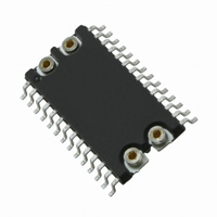
Packaging includes a 28-lead SOIC and
SNAPHAT® top (to be ordered separately)
■
SOIC package provides direct connection for a
SNAPHAT top contains the battery and crystal
■
Pin and function compatible with bq3285/7A
and DS12887
■
RoHS compliant
– Lead-free second level interconnect
December 2008
24
1
PCDIP24 (PC)
Battery/Crystal
CAPHAT
SNAPHAT (SH)
Battery/Crystal
28
1
SOH28 (MH)
Rev 7
This is information on a product still in production but not recommended for new designs.
1/36
www.st.com
1
�Contents
M48T86
Contents
1
Description . . . . . . . . . . . . . . . . . . . . . . . . . . . . . . . . . . . . . . . . . . . . . . . . . 6
2
Operation . . . . . . . . . . . . . . . . . . . . . . . . . . . . . . . . . . . . . . . . . . . . . . . . . . 9
2.1
Signal description . . . . . . . . . . . . . . . . . . . . . . . . . . . . . . . . . . . . . . . . . . . . 9
2.1.1
2.1.2
VCC, VSS . . . . . . . . . . . . . . . . . . . . . . . . . . . . . . . . . . . . . . . . . . . . . . . . . . . . . . . . . . . . . . 9
SQW (square wave output) . . . . . . . . . . . . . . . . . . . . . . . . . . . . . . . . . . . 9
)
s
(
t
c
u
d
o
)
r
s
(
P
t
c
e
t
u
e
d
l
o
o
r
s
P
b
e
O
t
e
l
)
o
s
(
s
t
b
c
u
O
d
o
)
r
s
P
(
t
c
e
t
u
e
l
d
o
o
r
s
P
b
O
e
t
e
l
o
s
b
O
3
2.1.3
AD0-AD7 (multiplexed bidirectional address/data bus) . . . . . . . . . . . . . . 9
2.1.4
AS (address strobe input) . . . . . . . . . . . . . . . . . . . . . . . . . . . . . . . . . . . . 9
2.1.5
MOT (mode select) . . . . . . . . . . . . . . . . . . . . . . . . . . . . . . . . . . . . . . . . 10
2.1.6
DS (data strobe input) . . . . . . . . . . . . . . . . . . . . . . . . . . . . . . . . . . . . . . 10
2.1.7
E (chip enable input) . . . . . . . . . . . . . . . . . . . . . . . . . . . . . . . . . . . . . . . 10
2.1.8
IRQ (interrupt request output) . . . . . . . . . . . . . . . . . . . . . . . . . . . . . . . . 10
2.1.9
RST (reset input) . . . . . . . . . . . . . . . . . . . . . . . . . . . . . . . . . . . . . . . . . . 10
2.1.10
RCL (RAM clear) . . . . . . . . . . . . . . . . . . . . . . . . . . . . . . . . . . . . . . . . . . 10
2.1.11
R/W (read/write input) . . . . . . . . . . . . . . . . . . . . . . . . . . . . . . . . . . . . . . 11
2.1.12
Non-volatile RAM . . . . . . . . . . . . . . . . . . . . . . . . . . . . . . . . . . . . . . . . . . 11
Clock operations . . . . . . . . . . . . . . . . . . . . . . . . . . . . . . . . . . . . . . . . . . . 14
3.1
Address map . . . . . . . . . . . . . . . . . . . . . . . . . . . . . . . . . . . . . . . . . . . . . . 14
3.2
Time, calendar, and alarm locations . . . . . . . . . . . . . . . . . . . . . . . . . . . . 14
3.3
Interrupts . . . . . . . . . . . . . . . . . . . . . . . . . . . . . . . . . . . . . . . . . . . . . . . . . 16
3.4
Periodic interrupt . . . . . . . . . . . . . . . . . . . . . . . . . . . . . . . . . . . . . . . . . . . 16
3.5
Alarm interrupt . . . . . . . . . . . . . . . . . . . . . . . . . . . . . . . . . . . . . . . . . . . . . 17
3.6
Update cycle interrupt . . . . . . . . . . . . . . . . . . . . . . . . . . . . . . . . . . . . . . . 17
3.7
Oscillator control bits . . . . . . . . . . . . . . . . . . . . . . . . . . . . . . . . . . . . . . . . 17
3.8
Update cycle . . . . . . . . . . . . . . . . . . . . . . . . . . . . . . . . . . . . . . . . . . . . . . . 17
3.9
Square wave output selection . . . . . . . . . . . . . . . . . . . . . . . . . . . . . . . . . 18
3.10
Register A . . . . . . . . . . . . . . . . . . . . . . . . . . . . . . . . . . . . . . . . . . . . . . . . . 19
3.11
3.10.1
UIP update in progress . . . . . . . . . . . . . . . . . . . . . . . . . . . . . . . . . . . . . 19
3.10.2
OSC0, OSC1, OSC2 oscillator control . . . . . . . . . . . . . . . . . . . . . . . . . 19
3.10.3
RS3, RS2, RS1, RS0 . . . . . . . . . . . . . . . . . . . . . . . . . . . . . . . . . . . . . . . 19
Register B . . . . . . . . . . . . . . . . . . . . . . . . . . . . . . . . . . . . . . . . . . . . . . . . . 20
3.11.1
2/36
SET . . . . . . . . . . . . . . . . . . . . . . . . . . . . . . . . . . . . . . . . . . . . . . . . . . . . 20
�M48T86
Contents
3.12
3.11.2
PIE: periodic interrupt enable . . . . . . . . . . . . . . . . . . . . . . . . . . . . . . . . 20
3.11.3
AIE: alarm interrupt enable . . . . . . . . . . . . . . . . . . . . . . . . . . . . . . . . . . 20
3.11.4
UIE: update ended interrupt enable . . . . . . . . . . . . . . . . . . . . . . . . . . . . 20
3.11.5
SQWE: square wave enable . . . . . . . . . . . . . . . . . . . . . . . . . . . . . . . . . 20
3.11.6
DM: data mode . . . . . . . . . . . . . . . . . . . . . . . . . . . . . . . . . . . . . . . . . . . 20
3.11.7
24/12 . . . . . . . . . . . . . . . . . . . . . . . . . . . . . . . . . . . . . . . . . . . . . . . . . . . 21
3.11.8
DSE: daylight savings enable . . . . . . . . . . . . . . . . . . . . . . . . . . . . . . . . 21
Register C . . . . . . . . . . . . . . . . . . . . . . . . . . . . . . . . . . . . . . . . . . . . . . . . 21
3.12.1
IRQF: interrupt request flag . . . . . . . . . . . . . . . . . . . . . . . . . . . . . . . . . . 21
)
s
(
t
c
u
d
o
)
r
s
(
P
t
c
e
t
u
e
d
l
o
o
r
s
P
b
e
O
t
e
l
)
o
s
(
s
t
b
c
u
O
d
o
)
r
s
P
(
t
c
e
t
u
e
l
d
o
o
r
s
P
b
O
e
t
e
l
o
s
b
O
3.13
3.14
3.12.2
PF: periodic interrupt flag . . . . . . . . . . . . . . . . . . . . . . . . . . . . . . . . . . . . 22
3.12.3
AF: alarm flag . . . . . . . . . . . . . . . . . . . . . . . . . . . . . . . . . . . . . . . . . . . . 22
3.12.4
UF: update ended interrupt flag . . . . . . . . . . . . . . . . . . . . . . . . . . . . . . . 22
3.12.5
BIT 0 through 3: unused bits . . . . . . . . . . . . . . . . . . . . . . . . . . . . . . . . . 22
Register D . . . . . . . . . . . . . . . . . . . . . . . . . . . . . . . . . . . . . . . . . . . . . . . . 22
3.13.1
VRT: valid RAM and time . . . . . . . . . . . . . . . . . . . . . . . . . . . . . . . . . . . . 22
3.13.2
BIT 0 through 6: unused bits . . . . . . . . . . . . . . . . . . . . . . . . . . . . . . . . . 22
VCC noise and negative going transients . . . . . . . . . . . . . . . . . . . . . . . . . 23
4
Maximum ratings . . . . . . . . . . . . . . . . . . . . . . . . . . . . . . . . . . . . . . . . . . . 24
5
DC and AC parameters . . . . . . . . . . . . . . . . . . . . . . . . . . . . . . . . . . . . . . 25
6
Package mechanical data . . . . . . . . . . . . . . . . . . . . . . . . . . . . . . . . . . . . 28
7
Part numbering . . . . . . . . . . . . . . . . . . . . . . . . . . . . . . . . . . . . . . . . . . . . 33
8
Environmental information . . . . . . . . . . . . . . . . . . . . . . . . . . . . . . . . . . . 34
9
Revision history . . . . . . . . . . . . . . . . . . . . . . . . . . . . . . . . . . . . . . . . . . . 35
3/36
�List of tables
M48T86
List of tables
Table 1.
Table 2.
Table 3.
Table 4.
Table 5.
Table 6.
Table 7.
Table 8.
Table 9.
Table 10.
Table 11.
Table 12.
Table 13.
Table 14.
Table 15.
Table 16.
Signal names . . . . . . . . . . . . . . . . . . . . . . . . . . . . . . . . . . . . . . . . . . . . . . . . . . . . . . . . . . . . 7
AC characteristics . . . . . . . . . . . . . . . . . . . . . . . . . . . . . . . . . . . . . . . . . . . . . . . . . . . . . . . . 13
Time, calendar, and alarm formats . . . . . . . . . . . . . . . . . . . . . . . . . . . . . . . . . . . . . . . . . . . 15
Square wave frequency/periodic interrupt rate . . . . . . . . . . . . . . . . . . . . . . . . . . . . . . . . . . 18
Register A MSB . . . . . . . . . . . . . . . . . . . . . . . . . . . . . . . . . . . . . . . . . . . . . . . . . . . . . . . . . 19
Register B MSB . . . . . . . . . . . . . . . . . . . . . . . . . . . . . . . . . . . . . . . . . . . . . . . . . . . . . . . . . 21
Register C MSB . . . . . . . . . . . . . . . . . . . . . . . . . . . . . . . . . . . . . . . . . . . . . . . . . . . . . . . . . 22
Register D MSB . . . . . . . . . . . . . . . . . . . . . . . . . . . . . . . . . . . . . . . . . . . . . . . . . . . . . . . . . 22
Absolute maximum ratings . . . . . . . . . . . . . . . . . . . . . . . . . . . . . . . . . . . . . . . . . . . . . . . . . 24
Operating and AC measurement conditions . . . . . . . . . . . . . . . . . . . . . . . . . . . . . . . . . . . . 25
Capacitance . . . . . . . . . . . . . . . . . . . . . . . . . . . . . . . . . . . . . . . . . . . . . . . . . . . . . . . . . . . . 26
DC characteristics. . . . . . . . . . . . . . . . . . . . . . . . . . . . . . . . . . . . . . . . . . . . . . . . . . . . . . . . 26
Power down/up mode AC characteristics . . . . . . . . . . . . . . . . . . . . . . . . . . . . . . . . . . . . . . 27
Power down/up trip points DC characteristics . . . . . . . . . . . . . . . . . . . . . . . . . . . . . . . . . . 27
PCDIP24 – 24-pin plastic DIP, battery CAPHAT™, package mechanical data . . . . . . . . . 29
SOH28 – 28-lead plastic small outline, 4-socket battery SNAPHAT®, package
mechanical data . . . . . . . . . . . . . . . . . . . . . . . . . . . . . . . . . . . . . . . . . . . . . . . . . . . . . . . . . 30
SH – 4-pin SNAPHAT® housing for 48 mAh battery and crystal, package
mechanical data . . . . . . . . . . . . . . . . . . . . . . . . . . . . . . . . . . . . . . . . . . . . . . . . . . . . . . . . . 31
SH – 4-pin SNAPHAT® housing for 120 mAh battery and crystal, package
mechanical data . . . . . . . . . . . . . . . . . . . . . . . . . . . . . . . . . . . . . . . . . . . . . . . . . . . . . . . . . 32
Ordering information scheme . . . . . . . . . . . . . . . . . . . . . . . . . . . . . . . . . . . . . . . . . . . . . . . 33
SNAPHAT® battery table . . . . . . . . . . . . . . . . . . . . . . . . . . . . . . . . . . . . . . . . . . . . . . . . . . 33
Document revision history . . . . . . . . . . . . . . . . . . . . . . . . . . . . . . . . . . . . . . . . . . . . . . . . . 35
)
s
(
t
c
u
d
o
)
r
s
(
P
t
c
e
t
u
e
d
l
o
o
r
s
P
b
e
O
t
e
l
)
o
s
(
s
t
b
c
u
O
d
o
)
r
s
P
(
t
c
e
t
u
e
l
d
o
o
r
s
P
b
O
e
t
e
l
o
s
b
O
Table 17.
Table 18.
Table 19.
Table 20.
Table 21.
4/36
�M48T86
List of figures
List of figures
Figure 1.
Figure 2.
Figure 3.
Figure 4.
Figure 5.
Figure 6.
Figure 7.
Figure 8.
Figure 9.
Figure 10.
Figure 11.
Figure 12.
Figure 13.
Figure 14.
Figure 15.
Figure 16.
Figure 17.
Figure 18.
Figure 19.
Logic diagram . . . . . . . . . . . . . . . . . . . . . . . . . . . . . . . . . . . . . . . . . . . . . . . . . . . . . . . . . . . . 6
24-pin DIP connections. . . . . . . . . . . . . . . . . . . . . . . . . . . . . . . . . . . . . . . . . . . . . . . . . . . . . 7
28-pin SOIC connections . . . . . . . . . . . . . . . . . . . . . . . . . . . . . . . . . . . . . . . . . . . . . . . . . . . 8
Block diagram . . . . . . . . . . . . . . . . . . . . . . . . . . . . . . . . . . . . . . . . . . . . . . . . . . . . . . . . . . . . 8
Intel bus read AC waveform . . . . . . . . . . . . . . . . . . . . . . . . . . . . . . . . . . . . . . . . . . . . . . . . 11
Intel bus write mode AC waveform . . . . . . . . . . . . . . . . . . . . . . . . . . . . . . . . . . . . . . . . . . . 11
Motorola bus read/write mode AC waveforms . . . . . . . . . . . . . . . . . . . . . . . . . . . . . . . . . . 12
Address map. . . . . . . . . . . . . . . . . . . . . . . . . . . . . . . . . . . . . . . . . . . . . . . . . . . . . . . . . . . . 15
Update period timing and UIP. . . . . . . . . . . . . . . . . . . . . . . . . . . . . . . . . . . . . . . . . . . . . . . 19
Update-ended/periodic interrupt relationship . . . . . . . . . . . . . . . . . . . . . . . . . . . . . . . . . . . 21
Supply voltage protection . . . . . . . . . . . . . . . . . . . . . . . . . . . . . . . . . . . . . . . . . . . . . . . . . . 23
AC testing load circuit (no IRQ) . . . . . . . . . . . . . . . . . . . . . . . . . . . . . . . . . . . . . . . . . . . . . 25
AC testing load circuit (with IRQ) . . . . . . . . . . . . . . . . . . . . . . . . . . . . . . . . . . . . . . . . . . . . 26
Power down/up mode AC waveforms. . . . . . . . . . . . . . . . . . . . . . . . . . . . . . . . . . . . . . . . . 27
PCDIP24 – 24-pin plastic DIP, battery CAPHAT™, package outline . . . . . . . . . . . . . . . . . 29
SOH28 – 28-lead plastic small outline, 4-socket SNAPHAT®, package outline . . . . . . . . . 30
SH – 4-pin SNAPHAT® housing for 48 mAh battery and crystal, package outline . . . . . . . 31
SH – 4-pin SNAPHAT® housing for 120 mAh battery and crystal, package outline . . . . . . 32
Recycling symbols . . . . . . . . . . . . . . . . . . . . . . . . . . . . . . . . . . . . . . . . . . . . . . . . . . . . . . . 34
)
s
(
t
c
u
d
o
)
r
s
(
P
t
c
e
t
u
e
d
l
o
o
r
s
P
b
e
O
t
e
l
)
o
s
(
s
t
b
c
u
O
d
o
)
r
s
P
(
t
c
e
t
u
e
l
d
o
o
r
s
P
b
O
e
t
e
l
o
s
b
O
5/36
�Description
1
M48T86
Description
The M48T86 is an industry standard real-time clock (RTC). The M48T86 is composed of a
lithium energy source, quartz crystal, write protection circuitry, and a 128-byte RAM array.
This provides the user with a complete subsystem packaged in either a 24-pin DIP
CAPHAT™ or 28-pin SNAPHAT® SOIC. Functions available to the user include a nonvolatile time-of-day clock, alarm interrupts, a one-hundred-year clock with programmable
interrupts, square wave output, and 128 bytes of non-volatile static RAM.
The 24-pin, 600 mil DIP CAPHAT houses the M48T86 silicon with a quartz crystal and a
long-life lithium button cell in a single package.
)
s
(
t
c
u
d
o
)
r
s
(
P
t
c
e
t
u
e
d
l
o
o
r
s
P
b
e
O
t
e
l
)
o
s
(
s
t
b
c
u
O
d
o
)
r
s
P
(
t
c
e
t
u
e
l
d
o
o
r
s
P
b
O
e
t
e
l
o
s
b
O
The 28-pin, 330 mil SOIC provides sockets with gold plated contacts at both ends for direct
connection to a separate SNAPHAT® housing containing the battery and crystal. The
unique design allows the SNAPHAT battery package to be mounted on top of the SOIC
package after the completion of the surface mount process.
Insertion of the SNAPHAT housing after reflow prevents potential battery and crystal
damage due to the high temperatures required for device surface-mounting. The SNAPHAT
housing is keyed to prevent reverse insertion.
The SOIC and battery packages are shipped separately in plastic anti-static tubes or in tape
& reel form.
For the 28-lead SOIC, the battery/crystal package part number is “M4T28-BR12SH” (see
Table 20 on page 33).
Figure 1.
Logic diagram
VCC
8
AD0-AD7
SQW
E
IRQ
R/W
DS
M48T86
AS
RST
RCL
MOT
VSS
AI01640
6/36
�M48T86
Description
Table 1.
Signal names
AD0-AD7
E
Multiplexed address/data bus
Chip enable input
R/W
WRITE enable input
DS
Data strobe input
AS
Address strobe input
RST
Reset Input
RCL
RAM clear input
MOT
Bus type select input
SQW
Square wave output
)
s
(
t
c
u
d
o
)
r
s
(
P
t
c
e
t
u
e
d
l
o
o
r
s
P
b
e
O
t
e
l
)
o
s
(
s
t
b
c
u
O
d
o
)
r
s
P
(
t
c
e
t
u
e
l
d
o
o
r
s
P
b
O
e
t
e
l
o
s
b
O
Figure 2.
IRQ
Interrupt request output
(open drain)
VCC
Supply voltage
VSS
Ground
NC
Not connected internally
24-pin DIP connections
MOT
NC
NC
AD0
AD1
AD2
AD3
AD4
AD5
AD6
AD7
VSS
1
24
2
23
3
22
4
21
5
20
6
19
M48T86
7
18
8
17
9
16
10
15
11
14
12
13
VCC
SQW
NC
RCL
NC
IRQ
RST
DS
NC
R/W
AS
E
AI01641
7/36
�Description
M48T86
Figure 3.
28-pin SOIC connections
NC
MOT
NC
NC
AD0
AD1
AD2
AD3
AD4
AD5
AD6
AD7
VSS
VSS
NC
VCC
SQW
NC
RCL
NC
IRQ
RST
DS
NC
R/W
AS
E
NC
28
1
2
27
26
3
4
25
5
24
6
23
7
22
M48T86
8
21
9
20
10
19
11
18
12
17
13
16
14
15
)
s
(
t
c
u
d
o
)
r
s
(
P
t
c
e
t
u
e
d
l
o
o
r
s
P
b
e
O
t
e
l
)
o
s
(
s
t
b
c
u
O
d
o
)
r
s
P
(
t
c
e
t
u
e
l
d
o
o
r
s
P
b
O
e
t
e
l
o
s
b
O
AI01642
Figure 4.
Block diagram
OSCILLATOR
E
VCC
VBAT
POWER
SWITCH
AND
WRITE
PROTECT
VCC
/8
/ 64
/ 64
PERIODIC INTERRUPT/SQUARE WAVE SELECTOR
POK
SQUARE WAVE
OUTPUT
SQW
IRQ
REGISTERS A,B,C,D
CLOCK/
CALENDAR
UPDATE
CLOCK CALENDAR,
AND ALARM RAM
RST
DOUBLE
BUFFERED
DS
R/W
AS
BUS
INTERFACE
BCD/BINARY
INCREMENT
RCL
STORAGE
REGISTERS
(114 BYTES)
AD0-AD7
AI01643
8/36
�M48T86
2
Operation
Operation
The M48T86 clock is driven by a quartz-controlled oscillator with a nominal frequency of
32,768 Hz. The devices are tested not to exceed 23 ppm (parts per million) oscillator
frequency error at 25°C, which equates to approximately ±1 minute per month. Automatic
deselection of the device ensures the data integrity is not compromised should VCC fall
below specified power-fail deselect voltage (VPFD) levels (see Figure 14 on page 27). The
automatic deselection of the device remains in effect upon power up for a period of 200ms
(max) after VCC rises above VPFD, provided that the real-time clock is running and the countdown chain is not reset. This allows sufficient time for VCC to stabilize and gives the system
clock a wake-up period so that a valid system reset can be established.
)
s
(
t
c
u
2.1
Signal description
d
o
)
r
s
(
P
t
c
e
t
u
e
d
l
o
o
r
s
P
b
e
O
t
e
l
)
o
s
(
s
t
b
c
u
O
d
o
)
r
s
P
(
t
c
e
t
u
e
l
d
o
o
r
s
P
b
O
e
t
e
l
o
s
b
O
The block diagram in Figure 4 on page 8 shows the pin connections and the major internal
functions of the M48T86.
2.1.1
VCC, VSS
DC power is provided to the device on these pins.The M48T86 uses a 5 V VCC.
2.1.2
SQW (square wave output)
During normal operation (e.g., valid VCC), the SQW pin can output a signal from one of 13
taps. The frequency of the SQW pin can be changed by programming Register A as shown
in Table 4 on page 18. The SQW signal can be turned on and off using the SQWE bit
(Register B; Bit 3). The SQW signal is not available when VCC is less than VPFD.
2.1.3
AD0-AD7 (multiplexed bidirectional address/data bus)
The M48T86 provides a multiplexed bus in which address and data information share the
same signal path. The bus cycle consists of two stages; first the address is latched, followed
by the data. Address/Data multiplexing does not slow the access time of the M48T86,
because the bus change from address to data occurs during the internal RAM access time.
Addresses must be valid prior to the falling edge of AS (see Figure 5 on page 11), at which
time the M48T86 latches the address present on AD0-AD7. Valid WRITE data must be
present and held stable during the latter portion of the R/W pulse (see Figure 6 on page 11).
In a READ cycle, the M48T86 outputs 8 bits of data during the latter portion of the DS pulse.
The READ cycle is terminated and the bus returns to a high impedance state upon a high
transition on R/W.
2.1.4
AS (address strobe input)
A positive going pulse on the Address Strobe (AS) input serves to demultiplex the bus. The
falling edge of AS causes the address present on AD0-AD7 to be latched within the
M48T86.
9/36
�Operation
2.1.5
M48T86
MOT (mode select)
The MOT pin offers the flexibility to choose between two bus types (see Figure 7 on
page 12). When connected to VCC, Motorola bus timing is selected. When connected to VSS
or left disconnected, Intel bus timing is selected. The pin has an internal pull-down
resistance of approximately 20 KΩ.
2.1.6
DS (data strobe input)
The DS pin is also referred to as READ (RD). A falling edge transition on the Data Strobe
(DS) input enables the output during a a READ cycle. This is very similar to an Output
Enable (G) signal on other memory devices.
)
s
(
t
c
u
d
o
)
r
s
(
P
t
c
e
t
u
e
d
l
o
o
r
s
P
b
e
O
t
e
l
)
o
s
(
s
t
b
c
u
O
d
o
)
r
s
P
(
t
c
e
t
u
e
l
d
o
o
r
s
P
b
O
e
t
e
l
o
s
b
O
2.1.7
E (chip enable input)
The chip enable pin must be asserted low for a bus cycle in the M48T86 to be accessed.
Bus cycles which take place without asserting E will latch the addresses present, but no
data access will occur.
2.1.8
IRQ (interrupt request output)
The IRQ pin is an open drain output that can be used as an interrupt input to a processor.
The IRQ output remains low as long as the status bit causing the interrupt is present and the
corresponding interrupt-enable bit is set. IRQ returns to a high impedance state whenever
Register C is read. The RST pin can also be used to clear pending interrupts. The IRQ bus
is an open drain output so it requires an external pull-up resistor to VCC.
2.1.9
RST (reset input)
The M48T86 is reset when the RST input is pulled low. With a valid VCC applied and a low
on RST, the following events occur:
1.
Periodic Interrupt Enable (PIE) bit is cleared to a zero (Register B; Bit 6);
2.
Alarm Interrupt Enable (AIE) bit is cleared to a zero (Register B; Bit 5);
3.
Update Ended Interrupt Request (UF) bit is cleared to a zero (Register C; Bit 4);
4.
Interrupt Request (IRQF) bit is cleared to a zero (Register C Bit 7);
5.
Periodic Interrupt Flag (PF) bit is cleared to a zero (Register C; Bit 6);
6.
The device is not accessible until RST is returned high;
7.
Alarm Interrupt Flag (AF) bit is cleared to a zero (Register C; Bit 5);
8.
The IRQ pin is in the high impedance state
9.
Square Wave Output Enable (SQWE) bit is cleared to zero (Register B; Bit 3); and
10. Update Ended Interrupt Enable (UIE) is cleared to a zero (Register B; Bit 4).
2.1.10
RCL (RAM clear)
The RCL pin is used to clear all 114 storage bytes, excluding clock and control registers, of
the array to FF(hex) value. The array will be cleared when the RCL pin is held low for at least
100 ms with the oscillator running. Usage of this pin does not affect battery load. This
function is applicable only when VCC is applied.
10/36
�M48T86
Operation
2.1.11
R/W (read/write input)
The R/W pin is used to latch data into the M48T86 and provides functionality similar to W in
other memory systems.
2.1.12
Non-volatile RAM
The 114 general-purpose non-volatile RAM bytes are not dedicated to any special function
within the M48T86. They can be used by the processor program as non-volatile memory
and are fully accessible during the update cycle.
Figure 5.
Intel bus read AC waveform
)
s
(
t
c
u
d
o
)
r
s
(
P
t
c
e
t
u
e
d
l
o
o
r
s
P
b
e
O
t
e
l
)
o
s
(
s
t
b
c
u
O
d
o
)
r
s
P
(
t
c
e
t
u
e
l
d
o
o
r
s
P
b
O
e
t
e
l
o
s
b
O
tCYC
AS
tASW
tASD
DS
tDSL
tDSH
R/W
tDAS
tCS
tOD
tCH
E
tAS
tAH
tDHR
AD0-AD7
AI01647
Figure 6.
Intel bus write mode AC waveform
tCYC
AS
tDAS
tASW
tASD
DS
tDSL
tDSH
R/W
tCS
tCH
E
tAS
tAH
tDW
tDHW
AD0-AD7
AI01648
11/36
�Operation
Figure 7.
M48T86
Motorola bus read/write mode AC waveforms
AS
tDAS
tASW
tASD
tCYC
DS
tDSL
tDSH
tRWS
tRWH
)
s
(
t
c
u
d
o
)
r
s
(
P
t
c
e
t
u
e
d
l
o
o
r
s
P
b
e
O
t
e
l
)
o
s
(
s
t
b
c
u
O
d
o
)
r
s
P
(
t
c
e
t
u
e
l
d
o
o
r
s
P
b
O
e
t
e
l
o
s
b
O
R/W
tCH
tCS
E
tAH
tDW
tAS
tDHW
AD0-AD7
(Write)
tAS
tOD
tAH
tDHR
AD0-AD7
(Read)
AI01649
12/36
�M48T86
Operation
Table 2.
AC characteristics
M48T86
Parameter(1)
Symbol
Unit
Min
Typ
Max
tCYC
Cycle time
160
ns
tDSL
Pulse width, data strobe low or R/W high
80
ns
tDSH
Pulse width, data strobe high or R/W low
55
ns
tRWH
R/W hold time
0
ns
tRWS
R/W setup time
10
ns
tCS
Chip select setup time
5
ns
tCH
Chip select hold time
0
ns
tDHR
READ data hold time
0
tDHW
WRITE data hold time
0
ns
tAS
Address setup time
20
ns
tAH
Address hold time
5
ns
tDAS
Delay time, data strobe to address strobe
rise
10
ns
tASW
Pulse width address strobe high
30
ns
tASD
Delay time, address strobe to data strobe
rise
35
ns
tOD
Output data delay time from data strobe
rise
tDW
WRITE setup time
tBUC
Delay time before update cycle
tPI(2)
Periodic interrupt time interval
tUC
Time of update cycle
)
s
(
t
c
u
d
o
)
r
s
(
P
t
c
e
t
u
e
d
l
o
o
r
s
P
b
e
O
t
e
l
)
o
s
(
s
t
b
c
u
O
d
o
)
r
s
P
(
t
c
e
t
u
e
l
d
o
o
r
s
P
b
O
e
t
e
l
o
s
b
O
25
50
30
ns
ns
244
–
ns
–
µs
–
1
µs
1. Valid for ambient operating temperature: TA = 0 to 70°C; VCC = 4.5 to 5.5 V (except where noted).
2. See Table 4 on page 18.
13/36
�Clock operations
3
Clock operations
3.1
Address map
M48T86
The address map of the M48T86 is shown in Figure 8. It consists of 114 bytes of user RAM,
10 bytes of RAM that contain the RTC time, calendar and alarm data, and 4 bytes which are
used for control and status. All bytes can be read or written to except for the following:
1.
Registers C & D are “Read only.”
2.
Bit 7 of Register A is “Read only.”
The contents of the four Registers A, B, C, and D are described in the “Registers” section.
)
s
(
t
c
u
d
o
)
r
s
(
P
t
c
e
t
u
e
d
l
o
o
r
s
P
b
e
O
t
e
l
)
o
s
(
s
t
b
c
u
O
d
o
)
r
s
P
(
t
c
e
t
u
e
l
d
o
o
r
s
P
b
O
e
t
e
l
o
s
b
O
3.2
Time, calendar, and alarm locations
The time and calendar information is obtained by reading the appropriate memory bytes.
The time, calendar, and alarm registers are set or initialized by writing the appropriate RAM
bytes. the contents of the time, calendar, and alarm bytes can be either binary or binarycoded decimal (BCD) format. Before writing the internal time, calendar, and alarm register,
the SET bit (Register B; Bit 7) should be written to a logic '1.' This will prevent updates from
occurring while access is being attempted. In addition to writing the time, calendar, and
alarm registers in a selected format (binary or BCD), the data mode (DM) bit (Register B; Bit
2), must be set to the appropriate logic level ('1' signifies binary data; '0' signifies binary
coded decimal (BCD data). All time, calendar, and alarm bytes must use the same data
mode. The SET bit should be cleared after the data mode bit has been written to allow the
real-time clock to update the time and calendar bytes. Once initialized, the real-time clock
makes all updates in the selected mode. The data mode cannot be changed without
reinitializing the ten data bytes. Table 3 on page 15 shows the binary and BCD formats of
the time, calendar, and alarm locations. The 24/12 bit (Register B; Bit 1) cannot be changed
without reinitializing the hour locations. When the 12-hour format is selected, a logic '1' in
the high order bit of the hours byte represents PM. The time, calendar, and alarm bytes are
always accessible because they are double-buffered. Once per second the ten bytes are
advanced by one second and checked for an alarm condition. If a READ of the time and
calendar data occurs during an update, a problem exists where data such as seconds,
minutes, or hours may not correlate. However, the probability of reading incorrect time and
calendar data is low. Methods of avoiding possible incorrect time and calendar READs are
reviewed later in this text.
14/36
�M48T86
Clock operations
Figure 8.
Address map
0
14
BYTES
00
CLOCK AND CONTROL
STATUS REGISTERS
0
SECONDS
1
SECONDS ALARM
2
MINUTES
MINUTES ALARM
13
0D
3
14
0E
4
HOURS
5
HOURS ALARM
6
DAY OF WEEK
7
DATE OF MONTH
8
MONTH
BCD OR
BINARY
FORMAT
)
s
(
t
c
u
d
o
)
r
s
(
P
t
c
e
t
u
e
d
l
o
o
r
s
P
b
e
O
t
e
l
)
o
s
(
s
t
b
c
u
O
d
o
)
r
s
P
(
t
c
e
t
u
e
l
d
o
o
r
s
P
b
O
e
t
e
l
o
s
b
O
114
BYTES
STORAGE REGISTERS
127
9
YEAR
10
REGISTER A
11
REGISTER B
12
REGISTER C
13
REGISTER D
7F
AI01650
Table 3.
Time, calendar, and alarm formats
Range
Address
RTC bytes
Decimal
Binary
BCD
0
Seconds
0-59
00-3B
00-59
1
Seconds alarm
0-59
00-3B
00-59
2
Minutes
0-59
00-3B
00-59
3
Minutes alarm
0-59
00-3B
00-59
Hours, 12-hrs
1-12
01-0C AM
81-8C PM
01-12 AM
81-92 PM
Hours, 24-hrs
0-23
00-17
00-23
Hours alarm, 12-hrs
1-12
01-0C AM
81-8C PM
01-12 AM
81-92 PM
Hours alarm, 24-hrs
0-23
00-17
00-23
6
Day of week (1 = Sun)
1-7
01-07
01-07
7
Day of month
1-31
01-1F
01-31
8
Month
1-12
01-0C
01-12
9
Year
0-99
00-63
00-99
4
5
15/36
�Clock operations
3.3
M48T86
Interrupts
The RTC plus RAM includes three separate, fully automatic sources of interrupt (alarm,
periodic, update-in-progress) available to a processor. The alarm interrupt can be
programmed to occur at rates from once per second to once per day. The periodic interrupt
can be selected from rates of 500 ms to 122 µs. The update-ended interrupt can be used to
indicate that an update cycle has completed.
The processor program can select which interrupts, if any, are going to be used. Three bits
in Register B enable the interrupts. Writing a logic '1' to an interrupt-enable bit (Register B;
Bit 6 = PIE; Bit 5 = AIE; Bit 4 = UIE) permits an interrupt to be initialized when the event
occurs. A '0' in an interrupt-enable bit prohibits the IRQ pin from being asserted from that
interrupt condition. If an interrupt flag is already set when an interrupt is enabled, IRQ is
immediately set at an active level, although the interrupt initiating the event may have
occurred much earlier. As a result, there are cases where the program should clear such
earlier initiated interrupts before first enabling new interrupts.
)
s
(
t
c
u
d
o
)
r
s
(
P
t
c
e
t
u
e
d
l
o
o
r
s
P
b
e
O
t
e
l
)
o
s
(
s
t
b
c
u
O
d
o
)
r
s
P
(
t
c
e
t
u
e
l
d
o
o
rinterrupt
s Periodic
3.4
P
b
O
e
t
e
l
o
s
b
O
When an interrupt event occurs, the related flag bit (Register C; Bit 6 = PF; Bit 5 = AF;
Bit 4 = UF) is set to a logic '1.' These flag bits are set independent of the state of the
corresponding enable bit in Register B and can be used in a polling mode without enabling
the corresponding enable bits. The interrupt flag bits are status bits which software can
interrogate as necessary.
When a flag is set, an indication is given to software that an interrupt event has occurred
since the flag bit was last read; however, care should be taken when using the flag bits as all
are cleared each time Register C is read. Double latching is included with Register C so that
bits which are set remain stable throughout the READ cycle. All bits which are set high are
cleared when read. Any new interrupts which are pending during the READ cycle are held
until after the cycle is completed. One, two, or three bits can be set when reading Register
C. Each utilized flag bit should be examined when read to ensure that no interrupts are lost.
The second flag bit usage method is with fully enabled interrupts. When an interrupt flag bit
is set and the corresponding enable bit is also set, the IRQ pin is asserted low. IRQ is
asserted as long as at least one of the three interrupt sources has its flag and enable bits
both set. The IRQF bit (Register C; Bit 7) is a '1' whenever the IRQ pin is being driven low.
Determination that the RTC initiated an interrupt is accomplished by reading Register C. A
logic '1' in the IRQF bit indicates that one or more interrupts have been initiated by the
M48T86. The act of reading Register C clears all active flag bits and the IRQF bit.
The periodic interrupt will cause the IRQ pin to go to an active state from once every 500 ms
to once every 122 µs. This function is separate from the alarm interrupt which can be output
from once per second to once per day. The periodic interrupt rate is selected using the same
Register A bits which select the square wave frequency (see Table 4 on page 18). Changing
the Register A bits affects both the square wave frequency and the periodic interrupt output.
However, each function has a separate enable bit in Register B. The periodic interrupt is
enabled by the PIE bit (Register B; Bit 6). The periodic interrupt can be used with software
counters to measure inputs, create output intervals, or await the next needed software
function.
16/36
�M48T86
3.5
Clock operations
Alarm interrupt
The alarm interrupt provides the system processor with an interrupt when a match is made
between the RTC's hours, minutes, and seconds bytes and the corresponding alarm bytes.
The three alarm bytes can be used in two ways. First, when the alarm time is written in the
appropriate hours, minutes, and seconds alarm locations, the alarm interrupt is initiated at
the specified time each day if the Alarm Interrupt Enable bit (Register B; Bit 5) is high. The
second use is to insert a “Don't care” state in one or more of the three alarm bytes. The
“Don't care” code is any hexadecimal value from C0 to FF. The two most significant bits of
each byte set the “Don't care” condition when at logic '1.' An alarm will be generated each
hour when the “Don't care” is are set in the hours byte. Similarly, an alarm is generated
every minute with “Don't care” codes in the hour and minute alarm bytes. The “Don't care”
codes in all three alarm bytes create an interrupt every second.
)
s
(
t
3.6
Update cycle interrupt
c
u
d
o
)
r
s
(
P
t
c
e
t
u
e
d
l
o
o
3.7
Oscillator control bits
r
s
P
b
e
O
t
e
l
)
o
s
(
s
t
b
c
u
O
d
o
)
3.8
Update r
cycle
s
P
(
t
c
e
t
u
e
l
d
o
o
r
s
P
b
O
e
t
e
l
o
s
b
O
After each update cycle, the Update Cycle Ended Flag bit (UF) (Register C; Bit 4) is set to a
'1.' If the Update Interrupt Enable bit (UIE) (Register B; Bit 4) is set to a '1,' and the SET bit
(Register B; Bit 7) is a '0,' then an interrupt request is generated at the end of each update
cycle.
When the M48T86 is shipped from the factory the internal oscillator is turned off. This
feature prevents the lithium energy cell from being discharged until it is installed in a system.
A pattern of “010” in Bits 4-6 of Register A will turn the oscillator on and enable the
countdown chain. A pattern of “11X” will turn the oscillator on, but holds the countdown
chain of the oscillator in reset. All other combinations of Bits 4-6 keep the oscillator off.
The M48T86 executes an update cycle once per second regardless of the SET bit (Register
B; Bit 7). When the SET bit is asserted, the user copy of the double buffered time, calendar,
and alarm bytes is frozen and will not update as the time increments. However, the time
countdown chain continues to update the internal copy of the buffer. This feature allows
accurate time to be maintained, independent of reading and writing the time, calendar, and
alarm buffers. This also guarantees that the time and calendar information will be
consistent. The update cycle also compares each alarm byte with the corresponding time
byte and issues an alarm if a match or if a “Don't care” code is present in all three positions.
There are three methods of accessing the real time clock that will avoid any possibility of
obtaining inconsistent time and calendar data. The first method uses the update-ended
interrupt. If enabled, an interrupt occurs after every update cycle which indicates that over
999ms are available to read valid time and date information. If this interrupt is used, the
IRQF Bit (Register C; Bit 7) should be cleared before leaving the interrupt routine.
A second method uses the Update-In-Progress (UIP) bit (Register A; Bit 7) to determine if
the update cycle is in progress. The UIP bit will pulse once per second. After the UIP bit
goes high, the update transfer occurs 244 µs later. If a low is read on the UIP bit, the user
has at least 244 µs before the time/calendar data will be changed. Therefore, the user
17/36
�Clock operations
M48T86
should avoid interrupt service routines that would cause the time needed to read valid
time/calendar data to exceed 244 µs.
The third method uses a periodic interrupt to determine if an update cycle is in progress.
The UIP bit is set high between the setting of the PF bit (Register C; Bit 6). Periodic
interrupts that occur at a rate greater than tBUC allow valid time and date information to be
reached at each occurrence of the periodic interrupt.The READs should be completed
within 1/(tPL/2 + tBUC) to ensure that data is not read during the update cycle.
3.9
Square wave output selection
Thirteen of the 15 divider taps are made available to a 1-of-15 selector, as shown in the
block diagram of Figure 4 on page 8. The purpose of selecting a divider tap is to generate a
square wave output signal on the SQW pin. The RS3-RS0 bits in Register A establish the
square wave output frequency. These frequencies are listed in Table 4 on page 18. The
SQW frequency selection shares the 1-of-15 selector with the periodic interrupt generator.
Once the frequency is selected, the output of the SQW pin can be turned on and off under
program control with the Square Wave Enabled (SQWE) bit.
)
s
(
t
c
u
d
o
)
r
s
(
P
t
c
e
t
u
e
d
l
o
o
r
s
P
b
e
O
t
e
l
)
o
s
(
s
t
b
c
u
O
d
o
)
r
s
P
(
t
c
e
t
u
e
l
d
o
o
r
s
P
b
O
e
t
e
l
o
s
b
O
Table 4.
Square wave frequency/periodic interrupt rate
Register A bits
18/36
Square wave
Units
Periodic interrupt
RS3
RS2
RS1
RS0
Frequency
Period
Units
0
0
0
0
None
0
0
0
1
256
Hz
3.90625
ms
0
0
1
0
128
Hz
7.8125
ms
0
0
1
1
8.192
kHz
122.070
us
0
1
0
0
4.096
kHz
244.141
us
0
1
0
1
2.048
kHz
488.281
us
0
1
1
0
1.024
kHz
976.5625
us
0
1
1
1
512
Hz
1.953125
ms
1
0
0
0
256
Hz
3.90625
ms
1
0
0
1
128
Hz
7.8125
ms
1
0
1
0
64
Hz
15.625
ms
1
0
1
1
32
Hz
31.25
ms
1
1
0
0
16
Hz
62.5
ms
1
1
0
1
8
Hz
125
ms
1
1
1
0
4
Hz
250
ms
1
1
1
1
2
Hz
500
ms
None
�M48T86
Clock operations
3.10
Register A
3.10.1
UIP update in progress
The Update in Progress (UIP) bit is a status flag that can be monitored. When the UIP bit is
'1,' the update transfer will soon occur (see Figure 9). When UIP is a '0,' the update transfer
will not occur for at least 244 µs. The time, calendar, and alarm information in RAM is fully
available for access when the UIP bit is '0.' The UIP bit is “Read only” and is not affected by
RST. Writing the SET bit in Register B to a '1' inhibits any update transfer and clears the UIP
Status bit.
3.10.2
OSC0, OSC1, OSC2 oscillator control
)
s
(
t
c
u
d
o
)
r
s
(
P
t
c
e
t
u
e
d
l
o
o
r
s
P
b
e
O
t
e
l
)
o
s
(
s
t
b
c
u
O
d
o
)
r
s
P
(
t
c
e
t
u
e
l
d
o
o
r
s
P
b
O
e
t
e
l
o
s
b
O
These three bits are used to control the oscillator and reset the countdown chain. A pattern
of “010” enables operation by turning on the oscillator and enabling the divider chain. A
pattern of 11X turns the oscillator on, but keeps the frequency divider disabled. When “010”
is written, the first update begins after 500 ms.
3.10.3
RS3, RS2, RS1, RS0
These four rate-selection bits select one of the 13 taps on the 15-stage divider or disable the
divider output. The tap selected may be used to generate an output square wave (SQW pin)
and/or a periodic interrupt. The user may do one of the following:
1.
Enable the interrupt with the PIE bit;
or
2.
Enable the SQW output with the SQWE bit;
or
3.
Enable both at the same time and same rate;
or
4.
Enable neither.
Table 4 on page 18 lists the periodic interrupt rates and the square wave frequencies that
may be chosen with the RS bits. These four READ/WRITE bits are not affected by RST.
Table 5.
Register A MSB
BIT7
BIT6
BIT5
BIT4
BIT3
BIT2
BIT1
BIT0
UIP
OSC2
OSC1
OSC0
RS3
RS2
RS1
RS0
Figure 9.
Update period timing and UIP
UPDATE PERIOD (1sec)
UIP
tBUC
tUC
AI01651
19/36
�Clock operations
3.11
Register B
3.11.1
SET
M48T86
When the SET bit is a '0,' the update transfer functions normally by advancing the counts
once per second. When the SET bit is written to a '1,' any update transfer is inhibited and
the program may initialize the time and calendar bytes without an update occurring. READ
cycles can be executed in a similar manner. SET is a READ/WRITE bit which is not modified
by RST or internal functions of the M48T86.
3.11.2
PIE: periodic interrupt enable
The Periodic Interrupt Enable bit (PIE) is a READ/WRITE bit which allows the Periodic
Interrupt Flag (PF) bit in Register C to cause the IRQ pin to be driven low (see Figure 10 on
page 21 for the relationship between PIE and UIE). When the PIE bit is set to '1,' periodic
interrupts are generated by driving the IRQ pin low at a rate specified by the RS3-RS0 bits
of Register A. A '0' in the PIE bit blocks the IRQ output from being driven by a periodic
interrupt, but the Periodic Flag (PF) bit is still set at the periodic rate. PIE is not modified by
any internal M48T86 functions, but is cleared to '0' on RST.
)
s
(
t
c
u
d
o
)
r
s
(
P
t
c
e
t
u
e
d
l
o
o
r
s
P
b
e
O
t
e
l
)
o
s
(
s
t
b
c
u
O
d
o
)
r
s
P
(
t
c
e
t
u
e
l
d
o
o
r
s
P
b
O
e
t
e
l
o
s
b
O
3.11.3
AIE: alarm interrupt enable
The Alarm Interrupt Enable (AIE) bit is a READ/WRITE bit which, when set to a '1,' permits
the Alarm Flag (AF) bit in Register C to assert IRQ. An alarm interrupt occurs for each
second that the three time bytes equal the three alarm bytes including a “Don't care” alarm
code of binary 1XXXXXXX. When the AIE bit is set to '0,' the AF bit does not initiate the IRQ
signal. The RST pin clears AIE to '0.' The internal functions of the M48T86 do not affect the
AIE Bit.
3.11.4
UIE: update ended interrupt enable
The Update Ended Interrupt Enable (UIE) bit is a READ/WRITE bit which enables the
Update End Flag (UF) bit in Register C to assert IRQ. A transition low on the RST pin or the
SET bit going high clears the UIE bit.
3.11.5
SQWE: square wave enable
When the Square Wave Enable (SQWE) bit is set to a '1,' a square wave signal is driven out
on the SQW pin. The frequency is determined by the rate-selection bits RS3-RS0. When the
SQWE bit is set to '0,' the SQW pin is held low. The SQWE bit is cleared by the RST pin.
SQWE is a READ/WRITE bit.
3.11.6
DM: data mode
The Data Mode (DM) bit indicates whether time and calendar information are in binary or
BCD format. The DM bit is set by the program to the appropriate format and can be read as
required. This bit is not modified by internal function or RST. A '1' in DM signifies binary data
and a '0' specifies binary coded decimal (BCD) data.
20/36
�M48T86
3.11.7
Clock operations
24/12
The 24/12 Control bit establishes the format of the hours byte. A '1' indicates the 24-hour
mode and a '0' indicates the 12-hour mode. This bit is READ/WRITE and is not affected by
internal functions or RST.
3.11.8
DSE: daylight savings enable
The Daylight Savings Enable (DSE) bit is a READ/WRITE bit which enables two special
updates when set to a '1.' On the first Sunday in April, the time increments from 1:59:59AM
to 3:00:00 AM. On the last Sunday in October, when the time reaches 1:59:59 AM, it
changes to 1:00:00 AM. These special updates do not occur when the DSE bit is a '0.' This
bit is not affected by internal functions or RST.
)
s
(
t
c
u
d
o
)
r
s
(
P
t
c
e
t
u
e
d
l
o
o
r
s
P
b
e
O
t
e
l
)
o
s
(
s
t
b
c
u
O
d
o
)
r
s
P
(
t
c
e
t
u
e
l
d
o
o
r
s
P
b
O3.12 Register
e C
t
e
l
o
s
b
O
Table 6.
Register B MSB
BIT7
BIT6
BIT5
BIT4
BIT3
BIT2
BIT1
BIT0
SET
PIE
AIE
UIE
SQWE
DM
24/12
DSE
Figure 10. Update-ended/periodic interrupt relationship
UPDATE PERIOD (1sec)
UIP
tBUC
tPI
tPI
tUC
tPI
PF
UF
AI01652B
3.12.1
IRQF: interrupt request flag
The Interrupt Request Flag (IRQF) bit is set to a '1' when one or more of the following are
true:
PF = PIE = 1
AF = AIE = 1
UF = UIE = 1
(e.g., IRQF = PF*PIE+AF*AIE+UF*UIE)
21/36
�Clock operations
3.12.2
M48T86
PF: periodic interrupt flag
The Periodic Interrupt Flag (PF) is a “Read only” bit which is set to a '1' when an edge is
detected on the selected tap of the divider chain. The RS3-RS0 bits establish the periodic
rate. PF is set to a '1' independent of the state of the PIE Bit. The IRQ signal is active and
will set the IRQF bit. The PF bit is cleared by a RST or a software READ of Register C.
3.12.3
AF: alarm flag
A '1' in the AF (Alarm Interrupt Flag) bit indicates that the current time has matched the
alarm time. If the AIE bit is also a '1,' the IRQ pin will go low and a '1' will appear in the IRQF
Bit. A RST or a READ of Register C will clear AF.
)
s
(
t
c
u
d
o
)
r
s
(
P
t
c
e
t
u
e
d
l
o
o
r
3.13
Register D
s
P
b
e
O
t
e
l
)
o
s
(
s
t
b
c
u
O
d
o
)
r
s
P
(
t
c
e
t
u
e
l
d
o
o
r
s
P
b
O
e
t
e
l
o
s
b
O
3.12.4
UF: update ended interrupt flag
The Update Ended Interrupt Flag (UF) bit is set after each update cycle. When the UIE bit is
set to a '1,' the '1' in the UF bit causes the IRQF bit to be a '1.' This will assert the IRQ pin.
UF is cleared by reading Register C or a RST.
3.12.5
BIT 0 through 3: unused bits
Bit 3 through Bit 0 are unused. These bits always read '0' and cannot be written.
3.13.1
VRT: valid RAM and time
The Valid RAM and Time (VRT) bit is set to the '1' state by STMicroelectronics prior to
shipment. This bit is not writable and should always be a '1' when read. If a '0' is ever
present, an exhausted internal lithium cell is indicated and both the contents of the RTC
data and RAM data are questionable. This bit is unaffected by RST.
3.13.2
BIT 0 through 6: unused bits
The remaining bits of Register D are not usable. They cannot be written and when read,
they will always read '0.'
Table 7.
BIT7
BIT6
BIT5
BIT4
BIT3
BIT2
BIT1
BIT0
IRQF
PF
AF
UF
0
0
0
0
Table 8.
22/36
Register C MSB
Register D MSB
BIT7
BIT6
BIT5
BIT4
BIT3
BIT2
BIT1
BIT0
VRT
0
0
0
0
0
0
0
�M48T86
3.14
Clock operations
VCC noise and negative going transients
ICC transients, including those produced by output switching, can produce voltage
fluctuations, resulting in spikes on the VCC bus. These transients can be reduced if
capacitors are used to store energy which stabilizes the VCC bus. The energy stored in the
bypass capacitors will be released as low going spikes are generated or energy will be
absorbed when overshoots occur. A ceramic bypass capacitor value of 0.1 µF (as shown in
Figure 11) is recommended in order to provide the needed filtering.
In addition to transients that are caused by normal SRAM operation, power cycling can
generate negative voltage spikes on VCC that drive it to values below VSS by as much as
one volt. These negative spikes can cause data corruption in the SRAM while in battery
backup mode. To protect from these voltage spikes, it is recommended to connect a
schottky diode from VCC to VSS (cathode connected to VCC, anode to VSS). Schottky diode
1N5817 is recommended for through hole and MBRS120T3 is recommended for surface
mount.
)
s
(
t
c
u
d
o
)
r
s
(
P
t
c
e
t
u
e
d
l
o
o
r
s
P
b
e
O
t
e
l
)
o
s
(
s
t
b
c
u
O
d
o
)
r
s
P
(
t
c
e
t
u
e
l
d
o
o
r
s
P
b
O
e
t
e
l
o
s
b
O
Figure 11. Supply voltage protection
VCC
VCC
0.1μF
DEVICE
VSS
AI02169
23/36
�Maximum ratings
4
M48T86
Maximum ratings
Stressing the device above the rating listed in the absolute maximum ratings table may
cause permanent damage to the device. These are stress ratings only and operation of the
device at these or any other conditions above those indicated in the Operating sections of
this specification is not implied. Exposure to absolute maximum rating conditions for
extended periods may affect device reliability. Refer also to the STMicroelectronics SURE
Program and other relevant quality documents.
Table 9.
Absolute maximum ratings
Symbol
Parameter
TA
Value
Ambient operating temperature
TSLD(1),(2),(3)
Input or output voltages
VCC
Supply voltage
PD
Power dissipation
°C
uc
–40 to 85
od
Lead solder temperature for 10 seconds
VIO
)
s
(
t
0 to 70
Storage temperature (VCC off, oscillator off)
TSTG
Unit
260
Pr
–0.3 to 7.0
e
t
e
l
o
s
b
–0.3 to 7.0
c
u
d
1
°C
°C
)
s
t(
o
r
P
V
V
W
1. For DIP package: soldering temperature not to exceed 260°C for 10 seconds (total thermal budget not to
exceed 150°C for longer than 30 seconds).
2. For SOH28 package, standard (SnPb) lead finish: reflow at peak temperature of 225°C (the time above
220°C must not exceed 20 seconds).
O
)
e
t
le
3. For SOH28 package, lead-free (Pb-free) lead finish: reflow at peak temperature of 260°C (the time above
255°C must not exceed 30 seconds).
Warning:
s
(
t
c
Negative undershoots below –0.3 V are not allowed on any
pin while in the battery backup mode.
u
d
o
r
P
e
t
e
l
o
s
b
O
s
b
O
24/36
r
P
e
t
e
l
o
)
s
(
ct
u
d
o
Warning:
o
s
b
O
-
Do NOT wave solder SOIC to avoid damaging SNAPHAT
sockets.
�M48T86
5
DC and AC parameters
DC and AC parameters
This section summarizes the operating and measurement conditions, as well as the DC and
AC characteristics of the device. The parameters in the following DC and AC Characteristic
tables are derived from tests performed under the measurement conditions listed in the
relevant tables. Designers should check that the operating conditions in their projects match
the measurement conditions when using the quoted parameters.
Table 10.
Operating and AC measurement conditions
Parameter
M48T86
Unit
)
s
(
t
c
u
d
o
)
r
s
(
P
t
c
e
t
u
e
d
l
o
o
r
s
P
b
e
O
t
e
l
)
o
s
(
s
t
b
c
u
O
d
o
)
r
s
P
(
t
c
e
t
u
e
l
d
o
o
r
s
P
b
O
e
t
e
l
o
s
b
O
Supply voltage (VCC)
4.5 to 5.5
V
0 to 70
°C
Load capacitance (CL)
100
pF
Input rise and fall times
≤5
ns
0 to 3
V
1.5
V
Ambient operating temperature (TA)
Input pulse voltages
Input and output timing ref. voltages
Note:
Output Hi-Z is defined as the point where data is no longer driven.
Figure 12. AC testing load circuit (no IRQ)
5V
960Ω
FOR ALL
OUTPUTS
EXCEPT IRQ
510Ω
50pF
AI01644
25/36
�DC and AC parameters
M48T86
Figure 13. AC testing load circuit (with IRQ)
5V
1.15kΩ
IRQ
)
s
(
t
c
u
d
o
)
r
s
(
P
t
c
e
t
u
e
d
l
o
o
r
s
P
b
e
O
t
e
l
)
o
s
(
s
t
b
c
u
O
d
o
)
r
s
P
(
t
c
e
t
u
e
l
d
o
o
r
s
P
b
O
e
t
e
l
o
s
b
O
130pF
AI01645
Table 11.
Capacitance
Parameter(1)(2)
Symbol
CIN
CIO(3)
Min
Max
Unit
Input capacitance
7
pF
Input / output capacitance
5
pF
1. Effective capacitance measured with power supply at 5 V; sampled only, not 100% tested.
2. At 25°C, f = 1 MHz.
3. Outputs deselected.
Table 12.
DC characteristics
Symbol
ILI
ILO
(2)
Parameter
Input leakage current
Output leakage current
Test Condition(1)
Min
Max
Unit
0V ≤ VIN ≤ VCC
±1
µA
0V ≤ VOUT ≤ VCC
±1
µA
Outputs open
15
mA
ICC
Supply current
VIL
Input low voltage
–0.3
0.8
V
VIH
Input high voltage
2.2
VCC + 0.3
V
IOL = 4 mA
0.4
V
Output low voltage (IRQ)
IOL = 0.5 mA
0.4
V
Output high voltage
IOH = –1 mA
Output low voltage
VOL
VOH
2.4
1. Valid for ambient operating temperature: TA = 0 to 70°C; VCC = 4.5 to 5.5 V (except where noted).
2. Outputs deselected.
26/36
V
�M48T86
DC and AC parameters
Figure 14. Power down/up mode AC waveforms
VCC
4.5V
VPFD
VSO
tF
tR
trec
E
)
s
(
t
c
u
d
o
)
r
s
(
P
t
c
e
t
u
e
d
l
o
o
r
s
P
b
e
O
t
e
l
)
o
s
(
s
t
b
c
u
O
d
o
)
r
s
P
(
t
c
e
t
u
e
l
d
o
o
r
s
P
b
O
e
t
e
l
o
s
b
O
AI01646
Table 13.
Power down/up mode AC characteristics
Parameter(1)
Symbol
Min
Max
Unit
tF(2)
VCC fall time
300
µs
tR
VCC rise time
100
µs
trec
VPFD to E high
20
200
ms
1. Valid for ambient operating temperature: TA = 0 to 70°C; VCC = 4.5 to 5.5 V (except where noted).
2. VCC fall time of less than tF may result in deselection/write protection not occurring until 200 µs after VCC passes VPFD.
Table 14.
P
Power down/up trip points DC characteristics
Parameter(1)(2)
Symbol
VPFD
Power-fail deselect voltage
VSO
Battery backup switchover voltage
tDR(3)
Expected data retention time
Min
Typ
4.0
Max
Unit
4.35
V
3.0
10
V
YEARS
1. Valid for ambient operating temperature: TA = 0 to 70°C; VCC = 4.5 to 5.5 V (except where noted).
2. All voltages referenced to VSS.
3. At 25°C, VCC = 0 V.
27/36
�Package mechanical data
6
M48T86
Package mechanical data
In order to meet environmental requirements, ST offers these devices in different grades of
ECOPACK® packages, depending on their level of environmental compliance. ECOPACK®
specifications, grade definitions and product status are available at: www.st.com.
ECOPACK® is an ST trademark.
)
s
(
t
c
u
d
o
)
r
s
(
P
t
c
e
t
u
e
d
l
o
o
r
s
P
b
e
O
t
e
l
)
o
s
(
s
t
b
c
u
O
d
o
)
r
s
P
(
t
c
e
t
u
e
l
d
o
o
r
s
P
b
O
e
t
e
l
o
s
b
O
28/36
�M48T86
Package mechanical data
Figure 15. PCDIP24 – 24-pin plastic DIP, battery CAPHAT™, package outline
A2
A
A1
B1
B
L
C
e1
eA
e3
D
N
)
s
(
t
c
u
d
o
)
r
s
(
P
t
c
e
t
u
e
d
l
o
o
r
s
P
b
e
O
t
e
l
)
o
s
(
s
t
b
c
u
O
d
o
)
r
s
P
(
t
c
e
t
u
e
l
d
o
o
r
s
P
b
O
e
t
e
l
o
s
b
O
E
1
Note:
PCDIP
Drawing is not to scale.
Table 15.
PCDIP24 – 24-pin plastic DIP, battery CAPHAT™, package mechanical
data
mm
inches
Symb
Typ
Min
Max
A
8.89
A1
Typ
Min
Max
9.65
0.3500
0.3799
0.38
0.76
0.0150
0.0299
A2
8.36
8.89
0.3291
0.3500
B
0.38
053
0.0150
0.0209
B1
1.14
1.78
0.0449
0.0701
C
0.20
0.31
0.0079
0.0122
D
34.29
34.80
1.3500
1.3701
E
17.83
18.34
0.7020
0.7220
e1
2.29
2.79
0.0902
0.1098
e3
25.15
30.73
0.9902
1.2098
eA
15.24
16.00
0.6000
0.6299
L
3.05
3.81
0.1201
0.1500
N
24
24
29/36
�Package mechanical data
M48T86
Figure 16. SOH28 – 28-lead plastic small outline, 4-socket SNAPHAT®, package
outline
A2
A
C
B
eB
e
CP
D
N
)
s
(
t
c
u
d
o
)
r
s
(
P
t
c
e
t
u
e
d
l
o
o
r
s
P
b
e
O
t
e
l
)
o
s
(
s
t
b
c
u
O
d
o
)
r
s
P
(
t
c
e
t
u
e
l
d
o
o
r
s
P
b
O
e
t
e
l
o
s
b
O
E
H
A1
α
L
1
SOH-A
Note:
Drawing is not to scale.
Table 16.
SOH28 – 28-lead plastic small outline, 4-socket battery SNAPHAT®, package
mechanical data
mm
inches
Symb
Typ
Min
A
Typ
Min
3.05
Max
0.1201
A1
0.05
0.36
0.0020
0.0142
A2
2.34
2.69
0.0921
0.1059
B
0.36
0.51
0.0142
0.0201
C
0.15
0.32
0.0059
0.0126
D
17.71
18.49
0.6972
0.7280
E
8.23
8.89
0.3240
0.3500
–
–
–
–
eB
3.20
3.61
0.1260
0.1421
H
11.51
12.70
0.4531
0.5000
L
0.41
1.27
0.0161
0.0500
a
0°
8°
0°
8°
N
28
e
CP
30/36
Max
1.27
0.0500
28
0.10
0.0039
�M48T86
Package mechanical data
Figure 17. SH – 4-pin SNAPHAT® housing for 48 mAh battery and crystal, package
outline
A1
A2
A3
A
eA
B
L
eB
D
)
s
(
t
c
u
d
o
)
r
s
(
P
t
c
e
t
u
e
d
l
o
o
r
s
P
b
e
O
t
e
l
)
o
s
(
s
t
b
c
u
O
d
o
)
r
s
P
(
t
c
e
t
u
e
l
d
o
o
r
s
P
b
O
e
t
e
l
o
s
b
O
E
SH
Note:
Drawing is not to scale.
Table 17.
SH – 4-pin SNAPHAT® housing for 48 mAh battery and crystal, package
mechanical data
mm
inches
Symb
Typ
Min
A
Max
Typ
Min
9.78
Max
0.3850
A1
6.73
7.24
0.2650
0.2850
A2
6.48
6.99
0.2551
0.2752
A3
0.38
0.0150
B
0.46
0.56
0.0181
0.0220
D
21.21
21.84
0.8350
0.8598
E
14.22
14.99
0.5598
0.5902
eA
15.55
15.95
0.6122
0.6280
eB
3.20
3.61
0.1260
0.1421
L
2.03
2.29
0.0799
0.0902
31/36
�Package mechanical data
M48T86
Figure 18. SH – 4-pin SNAPHAT® housing for 120 mAh battery and crystal, package
outline
A1
A2
A3
A
eA
B
L
eB
D
)
s
(
t
c
u
d
o
)
r
s
(
P
t
c
e
t
u
e
d
l
o
o
r
s
P
b
e
O
t
e
l
)
o
s
(
s
t
b
c
u
O
d
o
)
r
s
P
(
t
c
e
t
u
e
l
d
o
o
r
s
P
b
O
e
t
e
l
o
s
b
O
E
SHTK-A
Note:
Drawing is not to scale.
Table 18.
SH – 4-pin SNAPHAT® housing for 120 mAh battery and crystal, package
mechanical data
mm
inches
Symb
Typ
Min
A
Typ
Min
10.54
Max
0.415
A1
8.00
8.51
0.315
.0335
A2
7.24
8.00
0.285
0.315
A3
32/36
Max
0.38
0.015
B
0.46
0.56
0.018
0.022
D
21.21
21.84
0.835
0.860
E
17.27
18.03
0.680
.0710
eA
15.55
15.95
0.612
0.628
eB
3.20
3.61
0.126
0.142
L
2.03
2.29
0.080
0.090
�M48T86
7
Part numbering
Part numbering
Table 19.
Ordering information scheme
Example:
M48T
86
MH
1
E
Device type
M48T
Supply voltage and write protect voltage
86 = VCC = 4.5 to 5.5 V; VPFD = 4.2 to 4.5 V
)
s
(
t
c
u
d
o
)
r
s
(
P
t
c
e
t
u
e
d
l
o
o
r
s
P
b
e
O
t
e
l
)
o
s
(
s
t
b
c
u
O
d
o
)
r
s
P
(
t
c
e
t
u
e
l
d
o
o
r
s
P
b
O
e
t
e
l
o
s
b
O
Package
PC = PCDIP24
MH(1) = SOH28
Temperature range
1 = 0 to 70°C
Shipping method
For SOH28:
Blank = Tubes (Not for New Design - use E)
E = Lead-free package (ECOPACK®), tubes
F = Lead-free package (ECOPACK®), tape & reel
TR = Tape & reel (Not for New Design - use F)
For PCDIP24:
Blank = Tubes
1. The SOIC package (SOH28) requires the SNAPHAT® battery/crystal package which is ordered separately
under the part number “M4T28-BR12SH” in plastic tube or “M4T28-BR12SHTR” in tape & reel form (see
Table 20).
Warning:
Do not place the SNAPHAT battery package “M4TXXBR12SH” in conductive foam as it will drain the lithium
button-cell battery.
For other options, or for more information on any aspect of this device, please contact the
ST sales office nearest you.
Table 20.
SNAPHAT® battery table
Part number
Description
Package
M4T28-BR12SH
Lithium battery (48 mAh) SNAPHAT
SH
M4T32-BR12SH
Lithium battery (120 mAh) SNAPHAT
SH
33/36
�Environmental information
8
M48T86
Environmental information
Figure 19. Recycling symbols
)
s
(
t
c
u
d
o
)
r
s
(
P
t
c
e
t
u
e
d
l
o
o
r
s
P
b
e
O
t
e
l
)
o
s
(
s
t
b
c
u
O
d
o
)
r
s
P
(
t
c
e
t
u
e
l
d
o
o
r
s
P
b
O
e
t
e
l
o
s
b
O
This product contains a non-rechargeable lithium (lithium carbon monofluoride chemistry)
button cell battery fully encapsulated in the final product.
Recycle or dispose of batteries in accordance with the battery manufacturer's instructions
and local/national disposal and recycling regulations.
Please refer to the following web site address for additional information regarding
compliance statements and waste recycling.
Go to www.st.com/rtc, then select "Lithium Battery Recycling" from "Related Topics".
34/36
�M48T86
9
Revision history
Revision history
Table 21.
Document revision history
Date
Revision
Mar-1999
1
04-May-2000
1.1
31-Jul-2001
2
20-May-2002
2.1
01-Apr-2003
3
Changes
First Issue
Page layout changed
Reformatted; temp/voltage info. added to tables (Table 12, 2, 13,14)
Modify reflow time and temperature footnotes (Table 9)
V2.2 template applied; test condition updated (Table 14 )
)
s
(
t
c
u
d
o
)
r
s
(
P
t
c
e
t
u
e
d
l
o
o
r
s
P
b
e
O
t
e
l
)
o
s
(
s
t
b
c
u
O
d
o
)
r
s
P
(
t
c
e
t
u
e
l
d
o
o
r
s
P
b
O
e
t
e
l
o
s
b
O
02-Apr-2004
4
Reformatted; update Lead-free package information (Table 9,19)
20-Feb-2007
5
Updated cover page (features) and Section 2: Operation on page 9.
05-Jul-2007
6
Added RoHS compliant and lead-free second level interconnect
information to cover page and Section 6: Package mechanical data;
updated Figure 5 and 7.
7
Updated cover page as product “not recommended for new design”;
updated footnotes for Table 9; updated text in Section 6: Package
mechanical data; added Section 8: Environmental information; minor
formatting changes
04-Dec-2008
35/36
�M48T86
)
s
(
t
c
u
d
o
)
r
s
(
P
t
c
e
t
u
e
d
l
o
o
r
s
P
b
e
O
t
e
l
)
o
s
(
s
t
b
c
u
O
d
o
)
r
s
P
(
t
c
e
t
u
e
l
d
o
o
r
s
P
b
O
e
t
e
l
o
s
b
O
Please Read Carefully:
Information in this document is provided solely in connection with ST products. STMicroelectronics NV and its subsidiaries (“ST”) reserve the
right to make changes, corrections, modifications or improvements, to this document, and the products and services described herein at any
time, without notice.
All ST products are sold pursuant to ST’s terms and conditions of sale.
Purchasers are solely responsible for the choice, selection and use of the ST products and services described herein, and ST assumes no
liability whatsoever relating to the choice, selection or use of the ST products and services described herein.
No license, express or implied, by estoppel or otherwise, to any intellectual property rights is granted under this document. If any part of this
document refers to any third party products or services it shall not be deemed a license grant by ST for the use of such third party products
or services, or any intellectual property contained therein or considered as a warranty covering the use in any manner whatsoever of such
third party products or services or any intellectual property contained therein.
UNLESS OTHERWISE SET FORTH IN ST’S TERMS AND CONDITIONS OF SALE ST DISCLAIMS ANY EXPRESS OR IMPLIED
WARRANTY WITH RESPECT TO THE USE AND/OR SALE OF ST PRODUCTS INCLUDING WITHOUT LIMITATION IMPLIED
WARRANTIES OF MERCHANTABILITY, FITNESS FOR A PARTICULAR PURPOSE (AND THEIR EQUIVALENTS UNDER THE LAWS
OF ANY JURISDICTION), OR INFRINGEMENT OF ANY PATENT, COPYRIGHT OR OTHER INTELLECTUAL PROPERTY RIGHT.
UNLESS EXPRESSLY APPROVED IN WRITING BY AN AUTHORIZED ST REPRESENTATIVE, ST PRODUCTS ARE NOT
RECOMMENDED, AUTHORIZED OR WARRANTED FOR USE IN MILITARY, AIR CRAFT, SPACE, LIFE SAVING, OR LIFE SUSTAINING
APPLICATIONS, NOR IN PRODUCTS OR SYSTEMS WHERE FAILURE OR MALFUNCTION MAY RESULT IN PERSONAL INJURY,
DEATH, OR SEVERE PROPERTY OR ENVIRONMENTAL DAMAGE. ST PRODUCTS WHICH ARE NOT SPECIFIED AS "AUTOMOTIVE
GRADE" MAY ONLY BE USED IN AUTOMOTIVE APPLICATIONS AT USER’S OWN RISK.
Resale of ST products with provisions different from the statements and/or technical features set forth in this document shall immediately void
any warranty granted by ST for the ST product or service described herein and shall not create or extend in any manner whatsoever, any
liability of ST.
ST and the ST logo are trademarks or registered trademarks of ST in various countries.
Information in this document supersedes and replaces all information previously supplied.
The ST logo is a registered trademark of STMicroelectronics. All other names are the property of their respective owners.
© 2008 STMicroelectronics - All rights reserved
STMicroelectronics group of companies
Australia - Belgium - Brazil - Canada - China - Czech Republic - Finland - France - Germany - Hong Kong - India - Israel - Italy - Japan Malaysia - Malta - Morocco - Singapore - Spain - Sweden - Switzerland - United Kingdom - United States of America
www.st.com
36/36
�