M48Z32V
3.3V, 256Kbit (32Kbit x 8) ZEROPOWER® SRAM
Features
■
Integrated, ultra low power SRAM, and powerfail control circuit
■
READ cycle time equals WRITE cycle time
■
Automatic power-fail chip deselect and WRITE
protection
■
WRITE protect voltages:
(VPFD = Power-fail deselect voltage)
– M48Z32V: 2.7V ≤ VPFD ≤ 3.0V
■
Ultra-low standby current
■
RoHS COMPLIANT
–
Lead-free second level interconnect
P
e
et
l
o
s
Ob
c
u
d
44
1
e
t
e
l
o
s
)
s
t(
c
u
d
ro
)
s
t(
b
O
-
l
o
bs
o
r
P
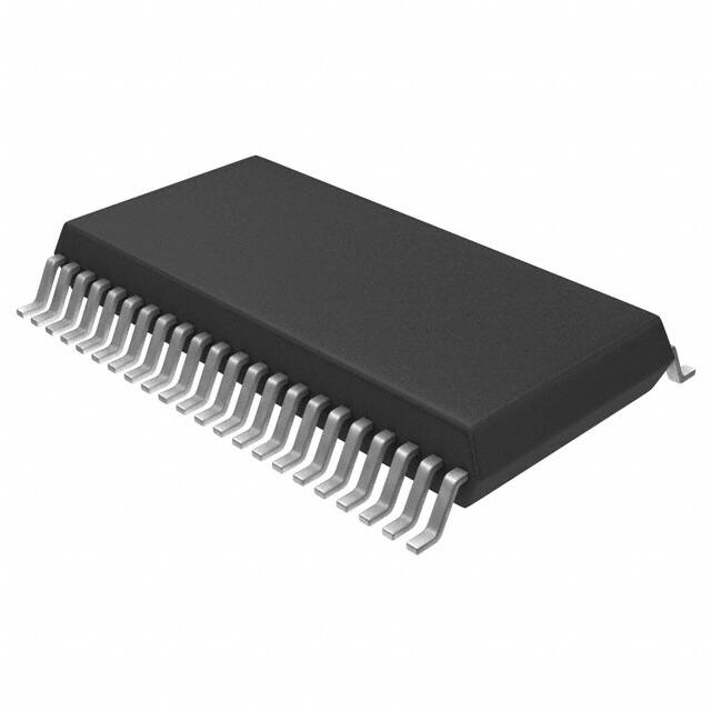
SO44 (MT)
44-pin SOIC
)
s
t(
c
u
d
o
r
P
e
et
O
)
s
(
t
c
u
d
o
r
eP
t
e
ol
s
b
O
November 2007
Rev 3
1/19
www.st.com
1
�Contents
M48Z32V
Contents
1
Summary . . . . . . . . . . . . . . . . . . . . . . . . . . . . . . . . . . . . . . . . . . . . . . . . . . 5
2
Operating modes . . . . . . . . . . . . . . . . . . . . . . . . . . . . . . . . . . . . . . . . . . . . 7
2.1
Read mode . . . . . . . . . . . . . . . . . . . . . . . . . . . . . . . . . . . . . . . . . . . . . . . . . 7
2.2
Write mode . . . . . . . . . . . . . . . . . . . . . . . . . . . . . . . . . . . . . . . . . . . . . . . . . 8
2.3
Data retention mode . . . . . . . . . . . . . . . . . . . . . . . . . . . . . . . . . . . . . . . . . 10
2.4
VCC noise and negative going transients . . . . . . . . . . . . . . . . . . . . . . . . . 11
)
s
t(
c
u
d
3
Maximum rating . . . . . . . . . . . . . . . . . . . . . . . . . . . . . . . . . . . . . . . . . . . . 12
4
DC and AC parameters . . . . . . . . . . . . . . . . . . . . . . . . . . . . . . . . . . . . . . 13
e
t
e
o
r
P
)
s
t(
c
u
d
o
6
Part numbering . . . . . . . . . . . . . . b
. . . . . . . . . . . . . . . . .r. . . . . . . . . . . . . 17
P
O
e
7
Revision history . . . . . .). . . . . . . . . . . . . . . . .t. . . . . . . . . . . . . . . . . . . . 18
le
s
(
o
t
s
c
b
u
d
O
o
r
)
P
s
t(
e
t
c
u
le
d
o
o
s
r
b
P
O
e
t
e
l
o
s
b
O
5
2/19
l
o
s
Package mechanical data . . . . . . . . . . . . . . . . . . . . . . . . . . . . . . . . . . . . 16
�M48Z32V
List of tables
List of tables
Table 1.
Table 2.
Table 3.
Table 4.
Table 5.
Table 6.
Table 7.
Table 8.
Table 9.
Table 10.
Table 11.
Table 12.
Table 13.
Table 14.
Table 15.
Signal names . . . . . . . . . . . . . . . . . . . . . . . . . . . . . . . . . . . . . . . . . . . . . . . . . . . . . . . . . . . . 5
Operating modes . . . . . . . . . . . . . . . . . . . . . . . . . . . . . . . . . . . . . . . . . . . . . . . . . . . . . . . . . 7
Read mode AC characteristics . . . . . . . . . . . . . . . . . . . . . . . . . . . . . . . . . . . . . . . . . . . . . . . 8
Write mode AC characteristics . . . . . . . . . . . . . . . . . . . . . . . . . . . . . . . . . . . . . . . . . . . . . . 10
Absolute maximum ratings . . . . . . . . . . . . . . . . . . . . . . . . . . . . . . . . . . . . . . . . . . . . . . . . . 12
Operating and AC measurement conditions . . . . . . . . . . . . . . . . . . . . . . . . . . . . . . . . . . . . 13
AC measurement load circuit . . . . . . . . . . . . . . . . . . . . . . . . . . . . . . . . . . . . . . . . . . . . . . . 13
Capacitance . . . . . . . . . . . . . . . . . . . . . . . . . . . . . . . . . . . . . . . . . . . . . . . . . . . . . . . . . . . . 13
DC characteristics. . . . . . . . . . . . . . . . . . . . . . . . . . . . . . . . . . . . . . . . . . . . . . . . . . . . . . . . 14
Power down/up mode AC waveforms. . . . . . . . . . . . . . . . . . . . . . . . . . . . . . . . . . . . . . . . . 14
Power down/up AC characteristics . . . . . . . . . . . . . . . . . . . . . . . . . . . . . . . . . . . . . . . . . . . 15
Power down/up trip points DC characteristics . . . . . . . . . . . . . . . . . . . . . . . . . . . . . . . . . . 15
SO44 – 44-lead plastic, small package mechanical data . . . . . . . . . . . . . . . . . . . . . . . . . . 16
Ordering information scheme . . . . . . . . . . . . . . . . . . . . . . . . . . . . . . . . . . . . . . . . . . . . . . . 17
Document revision history . . . . . . . . . . . . . . . . . . . . . . . . . . . . . . . . . . . . . . . . . . . . . . . . . 18
)
s
t(
c
u
d
e
t
e
l
o
s
)
s
t(
c
u
d
ro
P
e
et
l
o
s
Ob
b
O
-
l
o
bs
o
r
P
)
s
t(
c
u
d
o
r
P
e
et
O
)
s
(
t
c
u
d
o
r
eP
t
e
ol
s
b
O
3/19
�List of figures
M48Z32V
List of figures
Figure 1.
Figure 2.
Figure 3.
Figure 4.
Figure 5.
Figure 6.
Figure 7.
Figure 8.
Logic diagram . . . . . . . . . . . . . . . . . . . . . . . . . . . . . . . . . . . . . . . . . . . . . . . . . . . . . . . . . . . . 5
SOIC connections . . . . . . . . . . . . . . . . . . . . . . . . . . . . . . . . . . . . . . . . . . . . . . . . . . . . . . . . . 6
Block diagram . . . . . . . . . . . . . . . . . . . . . . . . . . . . . . . . . . . . . . . . . . . . . . . . . . . . . . . . . . . . 6
Read mode AC waveforms . . . . . . . . . . . . . . . . . . . . . . . . . . . . . . . . . . . . . . . . . . . . . . . . . . 8
Write enable controlled, write mode AC waveforms . . . . . . . . . . . . . . . . . . . . . . . . . . . . . . . 9
Chip enable controlled, write mode AC waveforms . . . . . . . . . . . . . . . . . . . . . . . . . . . . . . . 9
Supply voltage protection . . . . . . . . . . . . . . . . . . . . . . . . . . . . . . . . . . . . . . . . . . . . . . . . . . 11
SO44 – 44-lead plastic, small package outline . . . . . . . . . . . . . . . . . . . . . . . . . . . . . . . . . . 16
)
s
t(
c
u
d
e
t
e
l
o
s
)
s
t(
c
u
d
ro
P
e
et
l
o
s
Ob
s
b
O
t
e
ol
4/19
l
o
bs
O
)
s
(
t
c
u
d
o
r
eP
b
O
-
o
r
P
P
e
et
c
u
d
o
r
)
s
t(
�M48Z32V
1
Summary
Summary
The M48Z32V ZEROPOWER® RAM is a 32K x 8, non-volatile static RAM that integrates
power-fail deselect circuitry and battery control logic on a single die.
The 44-pin, 330mil SOIC provides a battery pin for an external, user-supplied battery. This is
all that is required to fully non-volatize the SRAM.
Figure 1.
Logic diagram
B+
VCC
15
DQ0-DQ7
W
M48Z32V
E
)
s
(
P
e
et
ol
bs
O
A0-A14
s
(
t
c
u
d
DQ0-DQ7
E
b
O
-
l
o
bs
VSS
o
r
P
)
s
t(
c
u
d
o
r
P
e
et
AI04787
O
)
Signal names
o
r
eP
t
e
l
o
s
Ob
t
c
u
d
o
r
e
t
e
l
o
s
G
c
u
d
8
A0-A14
Table 1.
)
s
t(
Address inputs
Data inputs / outputs
Chip enable input
G
Output enable input
W
WRITE enable input
VCC
Supply voltage
VSS
Ground
B+
Positive battery pin
NC
Not connected
5/19
�Summary
Figure 2.
M48Z32V
SOIC connections
A14
A12
A7
A6
A5
A4
NF
NC
NC
NC
NC
NC
NC
NC
A3
A2
A1
A0
DQ0
DQ1
DQ2
VSS
44
1
43
2
3
42
4
41
5
40
6
39
7
38
8
37
9
36
10
35
11
34
M48Z32V
12
33
13
32
14
31
15
30
16
29
17
28
27
18
19
26
20
25
21
24
22
23
)
s
t(
d
o
r
NF, Pin 7 must be tied to VSS.
P
e
et
Figure 3.
o
r
eP
Ob t
le
o
s
b
O
b
O
-
CE
DQ7
DQ6
DQ5
DQ4
DQ3
B+
l
o
bs
LITHIUM
CELL
c
u
d
o
r
P
)
s
t(
c
u
d
o
r
AI04786
O
)
A0-A14
POWER
VOLTAGE SENSE
AND
SWITCHING
CIRCUITRY
)
s
t(
P
e
et
s
(
t
c
u
d
Block diagram
l
o
s
e
t
e
l
o
s
uc
Note:
VCC
W
A13
A8
A9
A11
G
NC
NC
NC
NC
NC
NC
NC
A10
32K x 8
SRAM ARRAY
DQ0-DQ7
E
VPFD
W
G
USER
SUPPLIED
6/19
VCC
VSS
AI04788
�M48Z32V
2
Operating modes
Operating modes
The M48Z32V also has its own Power-fail Detect circuit. The control circuitry constantly
monitors the single power supply for an out of tolerance condition. When VCC is out of
tolerance, the circuit write protects the SRAM, providing a high degree of data security in the
midst of unpredictable system operation brought on by low VCC. As VCC falls below
approximately VSO, the control circuitry connects the battery which maintains data until valid
power returns.
Table 2.
Operating modes
Mode
VCC
Deselect
WRITE
3.0 to 3.6V
READ
READ
VSO to VPFD
Deselect
≤
Deselect
(min)(1)
VSO(1)
G
W
DQ0-DQ7
Power
VIH
X
X
High Z
Standby
VIL
X
VIL
DIN
VIL
VIL
VIH
DOUT
VIL
VIH
VIH
X
X
X
e
t
e
l
o
s
X
1. See Table 12 on page 15 for details.
X
b
O
-
X
Note:
X = VIH or VIL; VSO = Battery back-up switchover voltage.
2.1
Read mode
c
u
d
P
e
et
Ob
l
o
bs
od
uc
Pr
Active
Active
High Z
Active
High Z
CMOS standby
)
s
t(
Battery back-up
mode
c
u
d
o
r
High Z
P
e
et
The M48Z32V is in the READ Mode whenever W (WRITE Enable) is high, E (Chip Enable)
is low. The device architecture allows ripple-through access of data from eight of 262,144
locations in the static storage array. Thus, the unique address specified by the 15 Address
Inputs defines which one of the 32,768 bytes of data is to be accessed. Valid data will be
available at the Data I/O pins within Address Access time (tAVQV) after the last address input
signal is stable, providing that the E and G access times are also satisfied. If the E and G
access times are not met, valid data will be available after the latter of the Chip Enable
Access time (tELQV) or Output Enable Access time (tGLQV).
ro
l
o
s
)
s
t(
)
s
t(
E
O
)
s
(
t
c
u
d
o
r
eP
The state of the eight three-state Data I/O signals is controlled by E and G. If the outputs are
activated before tAVQV, the data lines will be driven to an indeterminate state until tAVQV. If
the Address Inputs are changed while E and G remain active, output data will remain valid
for Output Data Hold time (tAXQX) but will go indeterminate until the next Address Access.
t
e
ol
s
b
O
7/19
�Operating modes
Figure 4.
M48Z32V
Read mode AC waveforms
tAVAV
VALID
A0-A14
tAVQV
tAXQX
tELQV
tEHQZ
E
tELQX
tGLQV
tGHQZ
)
s
t(
G
c
u
d
tGLQX
DQ0-DQ7
VALID
Note:
WRITE Enable (W) = High.
Table 3.
Read mode AC characteristics
)
(s
ct
tAVAV
READ cycle time
tAVQV
Address valid to output valid
tELQV
Chip enable low to output valid
tGLQV
Output enable low to output valid
u
d
o
Ob
Pr
eP
s
(
t
c
u
d
Chip enable low to output transition
e
t
e
Output enable low to output transition
tEHQZ(2)
tGHQZ(2)
Chip enable high to output Hi-Z
ol
o
s
r
b
P
O
e
t
e
l
o
s Write mode
2.2
b
O
)
s
t(
M48Z32V
let
o
s
b
AI00925
c
u
d
o
r
O
)
tGLQX(2)
tAXQX
l
o
s
Parameter(1)
Symbol
tELQX(2)
e
t
e
o
r
P
–35
Min
Max
35
ns
35
ns
35
ns
15
ns
5
ns
0
ns
Output enable high to output Hi-Z
Address transition to output transition
Unit
5
13
ns
13
ns
0
ns
1. Valid for ambient operating temperature: TA = 0 to 70°C; Vcc = 3.0 to 3.6V (except where noted).
2. CL = 5pf (see Figure 8 on page 16).
The M48Z32V is in the WRITE Mode whenever W and E are low. The start of a WRITE is
referenced from the latter occurring falling edge of W or E. A WRITE is terminated by the
earlier rising edge of W or E. The addresses must be held valid throughout the cycle. E or W
must return high for a minimum of tEHAX from Chip Enable or tWHAX from WRITE Enable
prior to the initiation of another READ or WRITE cycle. Data-in must be valid tDVWH prior to
the end of WRITE and remain valid for tWHDX afterward. G should be kept high during
WRITE cycles to avoid bus contention; although, if the output bus has been activated by a
low on E and G, a low on W will disable the outputs tWLQZ after W falls.
8/19
�M48Z32V
Operating modes
Figure 5.
Write enable controlled, write mode AC waveforms
tAVAV
A0-A14
VALID
tAVWH
tWHAX
E
tWLWH
tAVWL
)
s
t(
W
c
u
d
tWHQX
tWLQZ
tWHDX
DQ0-DQ7
DATA INPUT
tDVWH
e
t
e
Figure 6.
l
o
s
b
O
VALID
A0-A14
ct
tAVEL
u
d
o
E
let
so
DQ0-DQ7
s
(
t
c
u
d
o
r
eP
l
o
bs
tAVEH
tELEH
P
e
et
tEHAX
O
)
tAVWL
r
P
e
W
)
s
(
)
s
t(
AI05662
c
u
d
o
r
Chip enable controlled, write mode AC waveforms
tAVAV
Ob
o
r
P
tEHDX
DATA INPUT
tDVEH
AI00927
t
e
ol
s
b
O
9/19
�Operating modes
M48Z32V
Table 4.
Write mode AC characteristics
M48Z32V
Parameter(1)
Symbol
–35
Min
Unit
Max
tAVAV
WRITE cycle time
35
ns
tAVWL
Address valid to WRITE enable low
0
ns
tAVEL
Address valid to chip enable low
0
ns
tWLWH
WRITE enable pulse width
25
ns
tELEH
Chip enable low to chip enable high
25
ns
tWHAX
WRITE enable high to address transition
0
tEHAX
Chip enable high to address transition
0
tDVWH
Input valid to WRITE enable high
12
tDVEH
Input valid to chip enable high
tWHDX
WRITE enable high to input transition
tEHDX
Chip enable high to input transition
tWLQZ(2)(3)
tAVWH
Address valid to WRITE enable high
tAVEH
Address valid to chip enable high
tWHQX(2)(3)
Ob
P
e
et
uc
ns
ns
ns
)
s
t(
0
ns
0
ns
c
u
d
o
r
13
ns
25
ns
25
ns
eP
WRITE enable high to output transition
)
(s
ns
d
o
r
12
l
o
s
WRITE enable low to output Hi-Z
)
s
t(
5
ns
t
e
l
o
s
b
1. Valid for ambient operating temperature: TA = 0 to 70°C; VCC = 3.0 to 3.6V (except where noted).
2. CL = 5pF (see Figure 8 on page 16).
t
c
u
3. If E goes low simultaneously with W going low, the outputs remain in the high impedance state.
d
o
r
2.3
O
)
Data retention mode
P
e
et
l
o
s
Ob
Note:
s
(
t
c
u
d
With valid VCC applied, the M48Z32V operates as a conventional BYTEWIDE™ static RAM.
Should the supply voltage decay, the RAM will automatically power-fail deselect, write
protecting itself when VCC falls within the VPFD (max), VPFD (min) window. All outputs
become high impedance, and all inputs are treated as “Don't care.”
o
r
eP
A power failure during a WRITE cycle may corrupt data at the currently addressed location,
but does not jeopardize the rest of the RAM's content. At voltages below VPFD(min), the
user can be assured the memory will be in a write protected state, provided the VCC fall time
is not less than tF. The M48Z32V may respond to transient noise spikes on VCC that reach
into the deselect window during the time the device is sampling VCC. Therefore, decoupling
of the power supply lines is recommended.
s
b
O
t
e
ol
When VCC drops below VSO, the control circuit switches power to the external battery which
preserves data.
As system power returns and VCC rises above VSO, the battery is disconnected, and the
power supply is switched to external VCC. Write protection continues until VCC reaches
VPFD(min) plus tREC(min). Normal RAM operation can resume tREC after VCC exceeds
VPFD(max).
For more information on Battery Storage Life refer to the Application Note AN1012.
10/19
�M48Z32V
2.4
Operating modes
VCC noise and negative going transients
ICC transients, including those produced by output switching, can produce voltage
fluctuations, resulting in spikes on the VCC bus. These transients can be reduced if
capacitors are used to store energy which stabilizes the VCC bus. The energy stored in the
bypass capacitors will be released as low going spikes are generated or energy will be
absorbed when overshoots occur. A ceramic bypass capacitor value of 0.1µF (see Figure 7)
is recommended in order to provide the needed filtering.
In addition to transients that are caused by normal SRAM operation, power cycling can
generate negative voltage spikes on VCC that drive it to values below VSS by as much as
one volt. These negative spikes can cause data corruption in the SRAM while in battery
backup mode. To protect from these voltage spikes, ST recommends connecting a schottky
diode from VCC to VSS (cathode connected to VCC, anode to VSS). (Schottky diode 1N5817
is recommended for through hole and MBRS120T3 is recommended for surface mount).
)
s
t(
Figure 7.
c
u
d
Supply voltage protection
o
r
P
VCC
e
t
e
VCC
l
o
s
0.1μF
)
s
t(
c
u
d
ro
P
e
et
l
o
s
Ob
b
O
-
c
u
d
o
r
DEVICE
P
e
et
VSS
l
o
bs
)
s
t(
AI02169
O
)
s
(
t
c
u
d
o
r
eP
t
e
ol
s
b
O
11/19
�Maximum rating
3
M48Z32V
Maximum rating
Stressing the device above the rating listed in the “Absolute Maximum Ratings” table may
cause permanent damage to the device. These are stress ratings only and operation of the
device at these or any other conditions above those indicated in the Operating sections of
this specification is not implied. Exposure to Absolute Maximum Rating conditions for
extended periods may affect device reliability. Refer also to the STMicroelectronics SURE
Program and other relevant quality documents.
Table 5.
Absolute maximum ratings
Symbol
Parameter
Ambient operating temperature
TA
Storage temperature (VCC Off, Oscillator Off)
TSTG
TSLD
(1)
Input or output voltages
VCC
Supply voltage
IO
Output current
PD
Power dissipation
Unit
Grade 1
0 to 70
SOIC
–55 to 125
Lead solder temperature for 10 seconds
VIO
)
s
t(
Value
uc
od
Pr
260
°C
°C
–0.3 to VCC + 0.3
°C
e
t
le
so
b
O
-
)
s
t(
–0.3 to 4.6
20
c
u
d
o
r
1
V
V
mA
W
1. For Lead-free (Pb-free) lead finish: Reflow at peak temperature of 260°C (total thermal budget not to exceed 245°C for
greater than 30 seconds).
Caution:
)
s
t(
c
u
d
ro
P
e
et
l
o
s
Ob
12/19
l
o
bs
O
)
s
(
t
c
u
d
o
r
eP
t
e
ol
s
b
O
P
e
et
Negative undershoots below –0.3V are not allowed on any pin while in the battery back-up
mode.
�M48Z32V
4
DC and AC parameters
DC and AC parameters
This section summarizes the operating and measurement conditions, as well as the DC and
AC characteristics of the device. The parameters in the following DC and AC Characteristic
tables are derived from tests performed under the Measurement Conditions listed in Table 6:
Operating and AC measurement conditions. Designers should check that the operating
conditions in their projects match the measurement conditions when using the quoted
parameters.
Table 6.
Operating and AC measurement conditions
Parameter(1)
Supply voltage (VCC)
3.0 to 3.6
Ambient operating temperature (TA)
Grade 1
Load Capacitance (CL)
Input rise and fall times
Input pulse voltages
e
t
le
Input and output timing ref. voltages
so
od
Pr
)
s
t(
DEVICE
UNDER
TEST
c
u
d
ro
eP
t
e
l
o
c
u
d
o
s
r
b
P
O
e
t
e
l
o
s
b
O
Table 8.
CIO
(3)
l
o
bs
645Ω
°C
50
pF
≤5
ns
)
s
t(
0 to 3
1.5
V
V
c
u
d
o
r
P
e
et
O
)
t(s
V
CL = 50pF or
5pF
CL includes JIG capacitance
1.75V
AI04789
Capacitance
Parameter(1)(2)
Max
Unit
Input capacitance
10
pF
Input / output capacitance
10
pF
Symbol
CIN
b
O
-
AC measurement load circuit
Unit
uc
0 to 70
1. Output Hi-Z is defined as the point where data is no longer driven.
Table 7.
)
s
t(
M48Z32V
Min
1. Effective capacitance measured with power supply at 3.3V; sampled only, not 100% tested.
2. At 25°C, f = 1MHz.
3. Outputs deselected.
13/19
�DC and AC parameters
Table 9.
DC characteristics
Sym
Test condition(1)
Parameter
ILI
ILO
M48Z32V
Input leakage current
(2)
Output leakage current
Min
Typ
Max
Unit
0V ≤ VIN ≤ VCC
±1
µA
0V ≤ VOUT ≤ VCC
±1
µA
1.2
µA
mA
Battery current
TA = 40°C; VCC = 0V
VBAT = 3V
ICC1
Supply current
IO = 0mA; Cycle Time = Min
E = 0.2V, other input =
VCC – 2V or 0.2V
45
ICC2
Supply current (TTL standby)
E = VIH
800
IBAT
0.2
ICC3
Supply current (CMOS standby)
VIL(3)
Input low voltage
E = VCC – 0.2V
–0.3
500
VIH
Input high voltage
2.2
VOL
Output low voltage
IOL = 2.1mA
VOH
Output high voltage
IOH = –1mA
d
o
r
t
e
l
o
3. Negative spikes of –1V allowed for up to 10ns once per cycle.
Table 10.
)-
s
(
t
c
VCC
VPFD (max)
VPFD (min)
u
d
o
VSO
e
t
e
l
o
s
INPUTS
Ob
14/19
Pr
tF
RECOGNIZED
t
e
ol
VALID
(PER CONTROL INPUT)
tFB
l
o
bs
O
)
s
(
t
c
u
d
tPD
o
r
eP
OUTPUTS
s
b
O
s
b
O
Power down/up mode AC waveforms
µA
V
VCC + 0.3
V
0.4
V
)
s
t(
V
1. Valid for ambient operating temperature: TA = 0 to 70°C; VCC = 3.0 to 3.6V (except where noted).
2. Outputs deselected.
µA
t
c
u
0.8
eP
0.8VCC
)
s
(
c
u
d
o
r
P
e
et
tR
tRB
tDR
tREC
DON'T CARE
RECOGNIZED
HIGH-Z
VALID
(PER CONTROL INPUT)
AI01168C
�M48Z32V
DC and AC parameters
Table 11.
Power down/up AC characteristics
Symbol
Parameter(1)
tPD
tF(2)
tFB(3)
tR
tRB
tREC
(4)
Min
E or W at VIH before power down
Max
Unit
0
µs
VPFD (max) to VPFD (min) VCC fall time
300
µs
VPFD (min) to VSS VCC fall time
10
µs
VPFD (min) to VPFD (max) VCC rise time
10
µs
VSS to VPFD (min) VCC rise time
1
µs
VPFD (max) to inputs recognized
40
200
ms
1. Valid for ambient operating temperature: TA = 0 to 70°C; VCC = 3.0 to 3.6V (except where noted).
)
s
t(
2. VPFD (max) to VPFD (min) fall time of less than tF may result in deselection/write protection not occurring
until 200µs after VCC passes VPFD (min).
c
u
d
3. VPFD (min) to VSS fall time of less than tFB may cause corruption of RAM data.
4. tREC (min) = 20ms for industrial temperature Grade (6) device.
Table 12.
Power down/up trip points DC characteristics
Parameter(1)(2)
Symbol
Min
VPFD
Power-fail deselect voltage
VSO
Battery back-up switchover voltage
1. All voltages referenced to VSS.
e
t
e
2.7
ol
s
b
O
o
r
P
Typ
Max
2.85
3.0
c
u
d
o
r
)
s
t(
VPFD – 100mV
Unit
V
V
P
e
et
2. Valid for ambient operating temperature: TA = 0 to 70°C or –40 to 85°C; VCC = 3.0 to 3.6V (except where
noted).
)-
s
(
t
c
u
d
o
r
P
e
t
e
l
o
l
o
bs
O
)
s
(
t
c
u
d
o
s
r
b
P
O
e
t
e
l
o
s
b
O
15/19
�Package mechanical data
5
M48Z32V
Package mechanical data
In order to meet environmental requirements, ST offers these devices in ECOPACK®
packages. These packages have a Lead-free second level interconnect. The category of
second Level Interconnect is marked on the package and on the inner box label, in
compliance with JEDEC Standard JESD97. The maximum ratings related to soldering
conditions are also marked on the inner box label. ECOPACK is an ST trademark.
ECOPACK specifications are available at: www.st.com.
Figure 8.
SO44 – 44-lead plastic, small package outline
A2
)
s
t(
A
c
u
d
C
B
e
CP
D
e
t
e
N
E
1
)
s
(
SOH-C
Note:
d
o
r
Table 13.
P
e
et
Symbol
ol
bs
O
α
L
t
e
l
o
s
b
O
)
Min
inch
Max
Typ
Min
3.05
Max
0.120
0.05
0.36
0.002
0.014
A2
2.34
2.69
0.092
0.106
B
0.36
0.46
0.014
0.018
C
0.15
0.32
0.006
0.012
D
17.71
18.49
0.697
0.728
E
8.23
8.89
0.324
0.350
–
–
–
–
H
11.51
12.70
0.453
0.500
L
0.41
1.27
0.016
0.050
a
0°
8°
0°
8°
N
44
e
CP
16/19
c
u
d
o
r
eP
A1
mm
s
(
t
c
u
d
Typ
o
r
eP
A1
b
O
-
)
s
t(
SO44 – 44-lead plastic, small package mechanical data
A
t
e
l
o
s
Ob
t
c
u
Drawing is not to scale.
l
o
s
H
o
r
P
0.81
0.032
44
0.10
0.004
�M48Z32V
6
Part numbering
Part numbering
Table 14.
Ordering information scheme
Example:
M48Z
32V
–35
MT
1
F
Device type
M48Z
)
s
t(
Supply voltage and write protect voltage
32V = VCC = 3.0 to 3.6V; VPFD = 2.7 to 3.0V
c
u
d
Speed
–35 = 35ns
e
t
e
Package
l
o
s
MT = 44-lead SOIC
Temperature range
)
s
t(
1 = 0 to 70°C
c
u
d
Shipping method
b
O
-
)
s
t(
c
u
d
o
r
P
e
et
O
)
E = Lead-free package (ECOPACK®), tubes
ro
l
o
bs
o
r
P
F = Lead-free package (ECOPACK®), tape & reel
P
e
et
l
o
s
Ob
s
(
t
c
u
d
For other options, or for more information on any aspect of this device, please contact the
ST sales office nearest you.
o
r
eP
t
e
ol
s
b
O
17/19
�Revision history
7
M48Z32V
Revision history
Table 15.
Document revision history
Date
Revision
Oct-2002
1.0
First Issue
07-Nov-2002
1.1
Update Absolute Maximum Ratings, DC Characteristics (Table 5, 8)
22-Mar-2004
2.0
Reformatted; updated Lead-free information (Table 5, 12)
3.0
Reformatted; added lead-free second level interconnect information
to cover page and Section 5: Package mechanical data; package
name change from SOH44 to SO44 throughout document; updated
Section 1: Summary; updated Table 3; 4, 5, 6, 9, 11, 13, 14 and
Figure 8.
02-Nov-2007
Changes
)
s
t(
c
u
d
e
t
e
l
o
s
)
s
t(
c
u
d
ro
P
e
et
l
o
s
Ob
s
b
O
t
e
ol
18/19
l
o
bs
O
)
s
(
t
c
u
d
o
r
eP
b
O
-
o
r
P
P
e
et
c
u
d
o
r
)
s
t(
�M48Z32V
)
s
t(
Please Read Carefully:
c
u
d
Information in this document is provided solely in connection with ST products. STMicroelectronics NV and its subsidiaries (“ST”) reserve the
right to make changes, corrections, modifications or improvements, to this document, and the products and services described herein at any
time, without notice.
All ST products are sold pursuant to ST’s terms and conditions of sale.
e
t
e
o
r
P
)
s
t(
c
u
d
o
r
Purchasers are solely responsible for the choice, selection and use of the ST products and services described herein, and ST assumes no
liability whatsoever relating to the choice, selection or use of the ST products and services described herein.
l
o
s
No license, express or implied, by estoppel or otherwise, to any intellectual property rights is granted under this document. If any part of this
document refers to any third party products or services it shall not be deemed a license grant by ST for the use of such third party products
or services, or any intellectual property contained therein or considered as a warranty covering the use in any manner whatsoever of such
third party products or services or any intellectual property contained therein.
)
s
t(
b
O
-
l
o
bs
P
e
et
UNLESS OTHERWISE SET FORTH IN ST’S TERMS AND CONDITIONS OF SALE ST DISCLAIMS ANY EXPRESS OR IMPLIED
WARRANTY WITH RESPECT TO THE USE AND/OR SALE OF ST PRODUCTS INCLUDING WITHOUT LIMITATION IMPLIED
WARRANTIES OF MERCHANTABILITY, FITNESS FOR A PARTICULAR PURPOSE (AND THEIR EQUIVALENTS UNDER THE LAWS
OF ANY JURISDICTION), OR INFRINGEMENT OF ANY PATENT, COPYRIGHT OR OTHER INTELLECTUAL PROPERTY RIGHT.
c
u
d
ro
O
)
UNLESS EXPRESSLY APPROVED IN WRITING BY AN AUTHORIZED ST REPRESENTATIVE, ST PRODUCTS ARE NOT
RECOMMENDED, AUTHORIZED OR WARRANTED FOR USE IN MILITARY, AIR CRAFT, SPACE, LIFE SAVING, OR LIFE SUSTAINING
APPLICATIONS, NOR IN PRODUCTS OR SYSTEMS WHERE FAILURE OR MALFUNCTION MAY RESULT IN PERSONAL INJURY,
DEATH, OR SEVERE PROPERTY OR ENVIRONMENTAL DAMAGE. ST PRODUCTS WHICH ARE NOT SPECIFIED AS "AUTOMOTIVE
GRADE" MAY ONLY BE USED IN AUTOMOTIVE APPLICATIONS AT USER’S OWN RISK.
P
e
et
l
o
s
s
(
t
c
u
d
o
r
eP
Resale of ST products with provisions different from the statements and/or technical features set forth in this document shall immediately void
any warranty granted by ST for the ST product or service described herein and shall not create or extend in any manner whatsoever, any
liability of ST.
Ob
t
e
ol
O
bs
ST and the ST logo are trademarks or registered trademarks of ST in various countries.
Information in this document supersedes and replaces all information previously supplied.
The ST logo is a registered trademark of STMicroelectronics. All other names are the property of their respective owners.
© 2007 STMicroelectronics - All rights reserved
STMicroelectronics group of companies
Australia - Belgium - Brazil - Canada - China - Czech Republic - Finland - France - Germany - Hong Kong - India - Israel - Italy - Japan Malaysia - Malta - Morocco - Singapore - Spain - Sweden - Switzerland - United Kingdom - United States of America
www.st.com
19/19
�