M5481
LED DISPLAY DRIVER
FEATURES SUMMARY
■ 2 DIGIT LED DRIVER (14 segments)
through a variable resistor connected either to VDD
or to a separate supply of 13.2V maximum.
The M5481 is a pin-to-pin replacement of the NS
MM 5481.
CURRENT GENERATOR OUTPUTS (no
registor required)
■
■
CONTINUOUS BRIGHTNESS CONTROL
■
SERIAL DATA INPUT
■
DATA ENABLE
■
WIDE SUPPLY VOLTAGE OPERATION
■
TLL COMPATIBILITY
■
APPLICATION EXAMPLES
■
MICROPROCESSOR DISPLAYS
■
INDUSTRIAL CONTROL INDICATOR
■
RELAY DRIVER
■
INSTRUMENTATION READOUTS
Figure 1. Package
c
u
d
e
t
le
o
r
P
PDIP20
(Plastic package)
b
O
-
DESCRIPTION
The M5481 is a monolithic MOS integrated circuit
produced with a N-channel silicon gate technology. It uses the M5450 die packaged in a 20-pin
plastic package copper frame, making it ideal for a
1-digit display. A single pin controls the LED display brightness by setting a reference current
)
s
(
ct
so
)
s
t(
u
d
o
r
P
e
Figure 2. Pin Connections
t
e
l
o
bs
O
Output Bit 8
Output Bit 7
1
20
Output Bit 9
2
19
Output Bit 10
Output Bit 6
3
18
Output Bit 11
Output Bit 5
4
17
Output Bit 12
Output Bit 4
5
16
Output Bit 13
Output Bit 3
6
15
VSS
Output Bit 2
7
14
Output Bit 1
8
13
Output Bit 14
Data Enable
Brightness Control
9
12
Data In
10
11
Clock
VDD
REV. 2
April 2004
1/10
�M5481
Figure 3. Block Diagram
VDD
Brightness
Control
10
Output
Bit 14
Output
Bit 1
14
8
100k
9
35 Output Buffers
1nF
Load
35 Latches
Data Enable
13
Serial Data
12
35-Bit Shift Register
Reset
11
Clock
15
e
t
le
Table 1. Absolute Maximum Ratings
Symbol
Parameter
VDD
– 0.3 to 15
V
15
V
40
mA
Total Package Power Dissipation at 25°C
1.5
W
Total Package Power Dissipation at 85°C
800
mW
Junction Temperature
150
°C
– 25 to 85
°C
– 65 to 150
°C
o
r
P
e
t
e
l
o
bs
V
(s)
ct
du
Output Sink Current
PTOT
TSTG
– 0.3 to 15
Off State Output Voltage
IO
TOP
Unit
Input Voltage
VO(off)
o
r
P
Value
Supply Voltage
VI
Tj
o
s
b
O
-
c
u
d
)
s
t(
Operating Temperature Range
Storage Temperature Range
Note: Stresses exceeding those listed under “Absolute Maximum Ratings” may cause permanent damage to the device and affect its reliability.
O
2/10
�M5481
Table 2. Static Electrical Characteristics
(Tamb within operating range, VDD = 4.75V to 13.2V, VSS = 0V, unless otherwise specified)
Symbol
Parameter
Test Conditions
VDD
Supply Voltage
IDD
Supply Current
VDD = 13.2V
VI
Input Voltage Logical "0" Level
± 10µA Input Bias
4.75 ≤ VDD ≤ 5.25
Logical "1" Level
VDD > 5.25
IB
Brightness Input Current (note 2)
VB
Brightness Input Voltage (pin 9)
VO(off)
IO
Input Current = 750µA, Tamb = 25°C
Max.
Unit
4.5
Typ.
13.2
V
7
mA
- 0.3
0.8
V
2.2
VDD
V
VDD - 2
VDD
V
0
0.75
3
4.3
Off State Out. Voltage
mA
V
13.2
V
10
µA
10
µA
Out. Sink Current (note 3)
Segment OFF
VO = 3V
Segment ON
VO = 1V (note 4)
Brightness In. = 0µA
fclock
IO
Note: 1.
2.
3.
4.
Min.
0
Brightness In. = 100µA
2
2,7
Brightness In. = 750µA
12
15
Input Clock Frequency
Output Matching (note 1)
mA
mA
0.5
MHz
± 20
%
c
u
d
0
)
s
t(
4
25
o
r
P
Output matching is calculated as the percent variation from I MAX + IMIN/2.
With a fixed resistor on the brightness input some variation in brightness will occur from one device to another.
Absolute maximum for each output should be limited to 40mA.
The VO voltage should be regulated by the user.
o
s
b
O
-
FUNCTIONAL DESCRIPTION
The M5481 uses the M5450 die which is packaged
to operate 2-digit alphanumeric displays with minimal interface with the display and the data source.
Serial data transfer from the data source to the display driver is accomplished with 2 signals, serial
data and clock. using a format of a leading “1” followed by the 35 data bits allows data transfer without an additional load signal.
The 35 data bits are latched after the 36th bit is
complete, thus providing non-multiplexed, direct
drive to the display. Outputs change only if the serial data bits differ from the previous time. Display
brightness is determined by control of the output
current for LED displays. A 1nF capacitor should
)
s
(
ct
u
d
o
r
P
e
t
e
l
o
e
t
le
be connected to brightness control (pin 9) to prevent possible oscillations.
A block diagram is shown on Figure 3. The output
current is typically 20 times greater than the current into pin 9, which is set by an external variable
resistor.
The latter is an internal limiting resistor of 400Ω
nominal value.
Figure 4 shows the input data format. A start bit of
logical “1” precedes the 35 bits of data. At the 36th
clock a LOAD is generated synchronously with the
high state of the clock, which loads the 35 bits of
the shift registers into the latches.
s
b
O
3/10
�M5481
Figure 4. Input Data Format
1
36
CLOCK
START
BIT 1
BIT 34
BIT 35
DATA
LOAD
(INTERNAL)
RESET
(INTERNAL)
Tj = [(Vout) (ILED) (No. of segments) + VDD x 7mA]
x (80°C/W) + Tamb
where:
Tj = junction temperature (150°Cmax)
Vout = voltage at the LED driver outputs
ILED = LED current
80°C/W = thermal coefficient of the package
Tamb = ambiant temperature
At the low state of the clock a RESET signal is
generated which clears all the shift registers for
the next set of data. The shift registers are static
master slave configurations. There is no clear for
the master portion of the first shift register, thus allowing continuous operation.
There must be a complete set of 36 clocks or
the shift registers will not clear.
When power is first applied to the chip an internal
power ON reset signal is generated which resets
all registers and all latches. The START bit and the
first clock reset the chip to its normal operation.
Figure 5 shows the timing relationships between
Data, Clock and DATA ENABLE.
A maximum clock frequency of 0.5MHz is assumed.
Table 3 shows the Output Data Format for the
M5481. Because it uses only 14 of the possible
outputs, 21 of the bits (including bit 35 which was
already unused in the M5450) are “Don’t Cares” .
For applications where a lesser number of outputs
are used it is possible to either increase the current per output or operate the part at higher than
1V Vout.
The following equation can be used for calculations.
c
u
d
Figure 5.
e
t
le
o
r
P
o
s
b
O
-
)
s
(
ct
CLOCK
DATA
u
d
o
300ns (min.)
r
P
e
DATA ENABLE
t
e
l
o
s
b
O
)
s
t(
100ns (min.)
Table 3. Serial Data Bus / Outputs Correspondance
5451
35
34
33
32
31
30
29
28
27
26
25
24
23
22
21
20
19
18
START
5481
X
X
X
X
X
14
13
X
X
X
X
12
11
10
9
X
X
X
START
5450
17
16
15
14
13
12
11
10
9
8
7
6
5
4
3
2
1
START
5481
X
8
7
6
5
X
X
X
X
4
3
2
1
X
X
X
X
START
4/10
�M5481
TYPICAL APPLICATION
Figure 6. BASIC electronically tuned TV system
LED DISPLAY
14 SEGMENTS
M5481
DISPLAY DRIVER
KEYBOARD
PLL
SYNTHESIZER
PROCESSOR
c
u
d
POWER DISSIPATION OF THE IC
The power dissipation of the IC can be limited using different configurations.
Figure 7.
+VC
)
s
(
ct
R
u
d
o
ID
VD
t
e
l
o
r
P
e
VOUT
s
b
O
e
t
le
)
s
t(
o
r
P
In this application R must be chosen taking into account the worst operating conditions.
R is determined by the maximum number of segments activated.
o
s
b
O
-
V –V
–V
C
DMAX
OMIN
R = ---------------------------------------------------------------N
L
MAX D
The worst case condition for the device is when
roughly half of the maximum number of segments
are activated.
It must be checked that the total power dissipation
does not exceed the absolute maximum ratings of
the device.
In critical cases more resistors can be used in conjunction with groups of segments.In this case the
current variation in the single resistor is reduced
and Ptot limited.
5/10
�M5481
Figure 8.
Figure 9.
+VC
+VC
VOUT+ VD
In this configuration the drop on the serial connected diodes is quite stable if the diodes are properly
chosen.
The total power dissipation of the IC depends only,
in first approximation, on the number of segments
activated.
)
s
(
ct
u
d
o
r
P
e
t
e
l
o
s
b
O
6/10
c
u
d
)
s
t(
In this configuration VOUT+VD is constant. the total
power dissipation of the IC depends only on the
number of segments activated.
o
s
b
O
-
e
t
le
o
r
P
�M5481
PART NUMBERING
Table 4. Order Codes
Part Number
Package
M5481 B7
Temperature Range
PDIP
-25 to 85 °C
c
u
d
e
t
le
)
s
(
ct
)
s
t(
o
r
P
o
s
b
O
-
u
d
o
r
P
e
t
e
l
o
s
b
O
7/10
�M5481
PACKAGE MECHANICAL
Table 5. PDIP20 - Mechanical Data
Symbol
Typ
3.25
millimeters
Min
3.30
0.508
A
a1
B
b
b1
C
D
E
e
e3
e4
F
I
L
N
R1
R2
K
K1
K2
Z
1.39
0.381
0.20
5.20
24.9
7.8
2.29
22.60
7.36
6.22
3.42
3.17
0.457
0.254
5.33
25.15
8.5
2.54
22.86
7.62
6.35
3.68
3.30
7d
0.152
0.762
1.524
0.762
0.762
1.27
Max
3.35
Typ
0.128
1.65
0.533
0.30
5.46
25.4
9.1
2.79
23.11
7.87
6.50
3.93
3.42
0.055
0.015
0.008
0.205
0.980
0.307
0.090
0.890
0.290
0.245
0.135
0.125
e
t
le
1.34
Figure 10. PDIP20 - Package Dimensions
c
u
d
K
A
e
F
e3
E
D
Tie Bar Center
20
11
1
10
R2
Note: Drawing is not to scale
b1
C
L
B
Z
s
b
O
8/10
a1
b
R1
t
e
l
o
I
K2
r
P
e
)
s
t(
0.053
N
K1
u
d
o
0.065
0.021
0.012
0.215
1.000
0.358
0.110
0.910
0.310
0.255
0.155
0.135
o
r
P
e4
N
N
)
s
(
ct
Max
0.132
0.018
0.010
0.210
0.990
0.335
0.100
0.900
0.300
0.250
0.145
0.130
7d
0.006
0.030
0.060
0.030
0.030
0.050
R1
o
s
b
O
-
inches
Min
0.130
0.020
�M5481
REVISION HISTORY
Table 6. Revision History
Date
Revision
Description of Changes
October-2000
1
First Issue
14-Apr-2004
2
Stylesheet update. No content change.
c
u
d
e
t
le
)
s
(
ct
)
s
t(
o
r
P
o
s
b
O
-
u
d
o
r
P
e
t
e
l
o
s
b
O
9/10
�M5481
c
u
d
e
t
le
)
s
(
ct
)
s
t(
o
r
P
o
s
b
O
-
u
d
o
r
P
e
t
e
l
o
Information furnished is believed to be accurate and reliable. However, STMicroelectronics assumes no responsibility for the consequences
of use of such information nor for any infringement of patents or other rights of third parties which may result from its use. No license is granted
by implication or otherwise under any patent or patent rights of STMicroelectronics. Specifications mentioned in this publication are subject
to change without notice. This publication supersedes and replaces all information previously supplied. STMicroelectronics products are not
authorized for use as critical components in life support devices or systems without express written approval of STMicroelectronics.
s
b
O
The ST logo is a registered trademark of STMicroelectronics.
All other names are the property of their respective owners
© 2004 STMicroelectronics - All rights reserved
STMicroelectronics GROUP OF COMPANIES
Australia - Belgium - Brazil - Canada - China - Czech Republic - Finland - France - Germany - Hong Kong - India - Israel - Italy - Japan Malaysia - Malta - Morocco - Singapore - Spain - Sweden - Switzerland - United Kingdom - United States
www.st.com
10/10
�
很抱歉,暂时无法提供与“M5481B7”相匹配的价格&库存,您可以联系我们找货
免费人工找货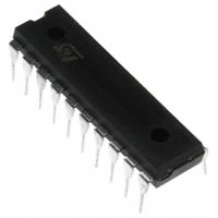


 工商网监
湘ICP备2023018690号
工商网监
湘ICP备2023018690号