M68AW512M
8 Mbit (512K x16) 3.0V Asynchronous SRAM
FEATURES SUMMARY
■ SUPPLY VOLTAGE: 2.7 to 3.6V
■
512K x 16 bits SRAM with OUTPUT ENABLE
■
EQUAL CYCLE and ACCESS TIME: 55ns
■
SINGLE BYTE READ/WRITE
■
LOW STANDBY CURRENT
■
LOW VCC DATA RETENTION: 1.5V
■
TRI-STATE COMMON I/O
■
AUTOMATIC POWER DOWN
October 2002
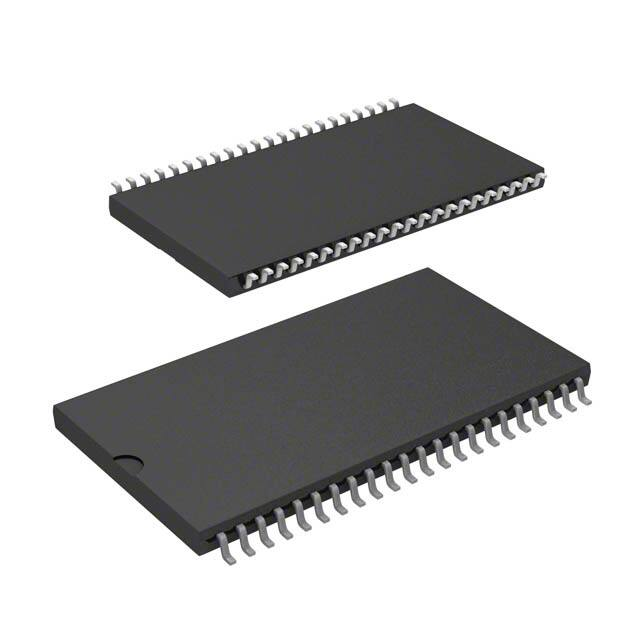
Figure 1. Package
44
1
TSOP44 Type II (ND)
1/18
�M68AW512M
TABLE OF CONTENTS
SUMMARY DESCRIPTION . . . . . . . . . . . . . . . . . . . . . . . . . . . . . . . . . . . . . . . . . . . . . . . . . . . . . . . . . . . 3
Figure 2. Logic Diagram . . . . . . . .
Table 1. Signal Names . . . . . . . . .
Figure 3. TSOP Connections. . . . .
Figure 4. Block Diagram . . . . . . . .
.......
.......
.......
.......
......................................
......................................
......................................
......................................
.....
.....
.....
.....
3
3
4
5
MAXIMUM RATING. . . . . . . . . . . . . . . . . . . . . . . . . . . . . . . . . . . . . . . . . . . . . . . . . . . . . . . . . . . . . . . . . 5
Table 2. Absolute Maximum Ratings . . . . . . . . . . . . . . . . . . . . . . . . . . . . . . . . . . . . . . . . . . . . . . . . . 5
DC AND AC PARAMETERS. . . . . . . . . . . . . . . . . . . . . . . . . . . . . . . . . . . . . . . . . . . . . . . . . . . . . . . . . . 6
Table 3. Operating and AC Measurement Conditions . . . . . . . . . . . . . . . . . . . . . . . . . . . . . . . . . . . . 6
Figure 5. AC Measurement I/O Waveform . . . . . . . . . . . . . . . . . . . . . . . . . . . . . . . . . . . . . . . . . . . . 6
Figure 6. AC Measurement Load Circuit . . . . . . . . . . . . . . . . . . . . . . . . . . . . . . . . . . . . . . . . . . . . . . 6
Table 4. Capacitance. . . . . . . . . . . . . . . . . . . . . . . . . . . . . . . . . . . . . . . . . . . . . . . . . . . . . . . . . . . . . 7
Table 5. DC Characteristics. . . . . . . . . . . . . . . . . . . . . . . . . . . . . . . . . . . . . . . . . . . . . . . . . . . . . . . . 7
OPERATION . . . . . . . . . . . . . . . . . . . . . . . . . . . . . . . . . . . . . . . . . . . . . . . . . . . . . . . . . . . . . . . . . . . . . . 8
Table 6. Operating Modes . . . . . . . . . . . . . . . . . . . . . . . . . . . . . . . . . . . . . . . . . . . . . . . . . . . . . . . . . 8
Read Mode . . . . . . . . . . . . . . . . . . . . . . . . . . . . . . . . . . . . . . . . . . . . . . . . . . . . . . . . . . . . . . . . . . . . 8
Figure 7. Address Controlled, Read Mode AC Waveforms . . . . . . . . . . . . . . . . . . . . . . . . . . . . . . . . 8
Figure 8. Chip Enable or Output Enable Controlled, Read Mode AC Waveforms. . . . . . . . . . . . . . . 9
Figure 9. Chip Enable or UB/LB Controlled, Standby Mode AC Waveforms . . . . . . . . . . . . . . . . . . 9
Table 7. Read and Standby Mode AC Characteristics . . . . . . . . . . . . . . . . . . . . . . . . . . . . . . . . . . 10
Write Mode . . . . . . . . . . . . . . . . . . . . . . . . . . . . . . . . . . . . . . . . . . . . . . . . . . . . . . . . . . . . . . . . . . . 11
Figure 10. Write Enable Controlled, Write AC Waveforms . . . . . . . . . . . . . . . . . . . . . . . . . . . . . . . 11
Figure 11. Chip Enable Controlled, Write AC Waveforms . . . . . . . . . . . . . . . . . . . . . . . . . . . . . . . . 12
Figure 12. UB/LB Controlled, Write AC Waveforms . . . . . . . . . . . . . . . . . . . . . . . . . . . . . . . . . . . . 12
Table 8. Write Mode AC Characteristics . . . . . . . . . . . . . . . . . . . . . . . . . . . . . . . . . . . . . . . . . . . . . 13
Figure 13. Low V CC Data Retention AC Waveforms . . . . . . . . . . . . . . . . . . . . . . . . . . . . . . . . . . . . 14
Table 9. Low V CC Data Retention Characteristics. . . . . . . . . . . . . . . . . . . . . . . . . . . . . . . . . . . . . . 14
PACKAGE MECHANICAL . . . . . . . . . . . . . . . . . . . . . . . . . . . . . . . . . . . . . . . . . . . . . . . . . . . . . . . . . . 15
Figure 14. TSOP44 Type II - 44 lead Plastic Thin Small Outline Type II, Package Outline . . . . . . 15
Table 10. TSOP 44 TypeII - 44 lead Plastic Thin Small Outline TypeII, Package Mechanical Data 15
PART NUMBERING . . . . . . . . . . . . . . . . . . . . . . . . . . . . . . . . . . . . . . . . . . . . . . . . . . . . . . . . . . . . . . . 16
Table 11. Ordering Information Scheme . . . . . . . . . . . . . . . . . . . . . . . . . . . . . . . . . . . . . . . . . . . . . 1 6
REVISION HISTORY . . . . . . . . . . . . . . . . . . . . . . . . . . . . . . . . . . . . . . . . . . . . . . . . . . . . . . . . . . . . . . . 17
Table 12. Document Revision History . . . . . . . . . . . . . . . . . . . . . . . . . . . . . . . . . . . . . . . . . . . . . . . 17
2/18
�M68AW512M
SUMMARY DESCRIPTION
The M68AW512M is a 8 Mbit (8,388,608 bit)
CMOS SRAM, organized as 524,288 words by 16
bits. The device features fully static operation requiring no external clocks or timing strobes, with
equal address access and cycle times. It requires
a single 2.7 to 3.6V supply. This device has an au-
tomatic power-down feature, reducing the power
consumption by over 99% when deselected.
The M68AW512M is available in TSOP44 Type II
packages.
Figure 2. Logic Diagram
Table 1. Signal Names
VCC
19
16
A0-A18
DQ0-DQ15
W
A0-A16
Address Inputs
DQ0-DQ15
Data Input/Output
E
Chip Enable
G
Output Enable
W
Write Enable
UB
Upper Byte Enable Input
LB
Lower Byte Enable Input
VCC
Supply Voltage
VSS
Ground
NC
Not Connected Internally
DU
Don’t Use as Internally Connected
E
M68AW512M
G
UB
LB
VSS
AI05835c
3/18
�M68AW512M
Figure 3. TSOP Connections
A4
A3
A2
A1
A0
E
DQ0
DQ1
DQ2
DQ3
VCC
VSS
DQ4
DQ5
DQ6
DQ7
W
A18
A17
A16
A15
A14
1
44
43
2
3
42
4
41
40
5
39
6
38
7
37
8
36
9
35
10
34
11
M68AW512M
33
12
32
13
31
14
30
15
29
16
28
17
27
18
26
19
20
25
21
24
22
23
AI05836c
4/18
A5
A6
A7
G
UB
LB
DQ15
DQ14
DQ13
DQ12
VSS
VCC
DQ11
DQ10
DQ9
DQ8
A8
A9
A10
A11
A12
A13
�M68AW512M
Figure 4. Block Diagram
VCC
VSS
A18
ROW
DECODER
MEMORY
ARRAY
A7
DQ15
(8)
I/O CIRCUITS
UB
COLUMN
DECODER
DQ0
(8)
LB
A0
A6
(8)
UB
W
E
UB
(8)
LB
LB
G
AI05838
MAXIMUM RATING
Stressing the device above the rating listed in the
Absolute Maximum Ratings table may cause permanent damage to the device. These are stress
ratings only and operation of the device at these or
any other conditions above those indicated in the
Operating sections of this specification is not im-
plied. Exposure to Absolute Maximum Rating conditions for periods greater than 1 sec periods may
affect device reliability. Refer also to the STMicroelectronics SURE Program and other relevant
quality documents.
Table 2. Absolute Maximum Ratings
Symbol
Value
Unit
20
mA
Ambient Operating Temperature
–55 to 125
°C
TSTG
Storage Temperature
–65 to 150
°C
VCC
Supply Voltage
–0.5 to 4.6
V
–0.5 to VCC +0.5
V
1
W
IO (1)
TA
VIO (2)
PD
Parameter
Output Current
Input or Output Voltage
Power Dissipation
Note: 1. One output at a time, not to exceed 1 second duration.
2. Up to a maximum operating VCC of 3.6V only.
5/18
�M68AW512M
DC AND AC PARAMETERS
This section summarizes the operating and measurement conditions, as well as the DC and AC
characteristics of the device. The parameters in
the following DC and AC Characteristic tables are
derived from tests performed under the Measure-
ment Conditions listed in the relevant tables. Designers should check that the operating conditions
in their projects match the measurement conditions when using the quoted parameters.
Table 3. Operating and AC Measurement Conditions
Parameter
M68AW512M
VCC Supply Voltage
2.7 to 3.6V
Range 1
0 to 70°C
Range 6
–40 to 85°C
Ambient Operating Temperature
Load Capacitance (CL)
30pF
Output Circuit Protection Resistance (R1)
3.0kΩ
Load Resistance (R2)
3.1kΩ
Input Rise and Fall Times
≤ 1ns/V
Input Pulse Voltages
0 to VCC
Input and Output Timing Ref. Voltages
VCC/2
Output Transition Timing Ref. Voltages
VRL = 0.3VCC; VRH = 0.7VCC
Figure 5. AC Measurement I/O Waveform
Figure 6. AC Measurement Load Circuit
VCC
I/O Timing Reference Voltage
R1
VCC
VCC/2
0V
DEVICE
UNDER
TEST
OUT
CL
Output Timing Reference Voltage
VCC
0V
R2
0.7VCC
0.3VCC
AI05831
CL includes probe and 1 TTLcapacitance
AI05832
6/18
�M68AW512M
Table 4. Capacitance
CIN
COUT
Test
Condition
Parameter(1,2)
Symbol
Max
Unit
VIN = 0V
8
pF
VOUT = 0V
10
pF
Max
Unit
70ns
35
mA
55ns
40
mA
4
mA
20
µA
Input Capacitance on all pins (except DQ)
Output Capacitance
Min
Note: 1. Sampled only, not 100% tested.
2. At TA = 25°C, f = 1 MHz, VCC = 3.0V.
Table 5. DC Characteristics
Symbol
Parameter
ICC1 (1,2)
Operating Supply Current
ICC2 (3)
Operating Supply Current
ISB
Standby Supply Current CMOS
ILI
Input Leakage Current
ILO
Output Leakage Current
VIH
Test Condition
VCC = 3.6V, f = 1/tAVAV,
IOUT = 0mA
Min
Typ
VCC = 3.6V, f = 1MHz,
IOUT = 0mA
VCC = 3.6V, f = 0,
E ≥ VCC –0.2V or
LB=UB ≥ VCC –0.2V
1
0V ≤ VIN ≤ VCC
–1
1
µA
0V ≤ VOUT ≤ VCC (4)
–1
1
µA
Input High Voltage
2.2
VCC + 0.3
V
VIL
Input Low Voltage
–0.3
0.6
V
VOH
Output High Voltage
IOH = –1.0mA
VOL
Output Low Voltage
IOL = 2.1mA
Note: 1.
2.
3.
4.
2.4
V
0.4
V
Average AC current, cycling at tAVAV minimum.
E = VIL, LB OR/AND UB = VIL, V IN = V IL OR VIH.
E ≤ 0.2V, LB OR/AND UB ≤ 0.2V, V IN ≤ 0.2V OR VIN ≥ VCC –0.2V.
Output disabled.
7/18
�M68AW512M
OPERATION
The M68AW512M has a Chip Enable power down
feature which invokes an automatic standby mode
whenever either Chip Enable is de-asserted
(E = High) or LB and UB are de-asserted (LB and
UB = High). An Output Enable (G) signal provides
a high speed tri-state control, allowing fast read/
write cycles to be achieved with the common I/O
data bus. Operational modes are determined by
device control inputs W, E, LB and UB as summarized in the Operating Modes table (see Table 6).
Table 6. Operating Modes
Operation
E
W
G
LB
UB
DQ0-DQ7
DQ8-DQ15
Power
Deselected
VIH
X
X
X
X
Hi-Z
Hi-Z
Standby (ISB)
Deselected
X
X
X
VIH
VIH
Hi-Z
Hi-Z
Standby (ISB)
Lower Byte Read
VIL
VIH
VIL
VIL
VIH
Data Output
Hi-Z
Active (ICC)
Lower Byte Write
VIL
VIL
X
VIL
VIH
Data Input
Hi-Z
Active (ICC)
Output Disabled
VIL
VIH
VIH
X
X
Hi-Z
Hi-Z
Active (ICC)
Upper Byte Read
VIL
VIH
VIL
VIH
VIL
Hi-Z
Data Output
Active (ICC)
Upper Byte Write
VIL
VIL
X
VIH
VIL
Hi-Z
Data Input
Active (ICC)
Word Read
VIL
VIH
VIL
VIL
VIL
Data Output
Data Output
Active (ICC)
Word Write
VIL
VIL
X
VIL
VIL
Data Input
Data Input
Active (ICC)
Note: 1. X = VIH or VIL.
Read Mode
The M68AW512M is in the Read mode whenever
Write Enable (W) is High with Output Enable (G)
Low, and Chip Enable (E) is asserted. This provides access to data from eight or sixteen, depending on the status of the signal UB and LB, of
the 8,388,608 locations in the static memory array,
specified by the 19 address inputs. Valid data will
be available at the eight or sixteen output pins
within t AVQV after the last stable address, providing G is Low and E is Low. If Chip Enable or Output
Enable access times are not met, data access will
be measured from the limiting parameter (tELQV,
tGLQV or t BLQV) rather than the address. Data out
may be indeterminate at tELQX, tGLQX and tBLQX
but data lines will always be valid at tAVQV.
Figure 7. Address Controlled, Read Mode AC Waveforms
tAVAV
A0-A18
VALID
tAVQV
DQ0-DQ7 and/or DQ8-DQ15
tAXQX
DATA VALID
AI05839
Note: E = Low, G = Low, W = High, UB = Low and/or LB = Low.
8/18
�M68AW512M
Figure 8. Chip Enable or Output Enable Controlled, Read Mode AC Waveforms.
tAVAV
A0-A18
VALID
tAVQV
tAXQX
tELQV
tEHQZ
E
tELQX
tGLQV
tGHQZ
G
tGLQX
VALID
DQ0-DQ15
tBLQV
tBHQZ
UB, LB
tBLQX
AI05840
Note: Write Enable (W) = High.
Figure 9. Chip Enable or UB/LB Controlled, Standby Mode AC Waveforms
E, UB, LB
ICC
ISB
tPU
tPD
50%
AI03856
9/18
�M68AW512M
Table 7. Read and Standby Mode AC Characteristics
M68AW512M
Symbol
Parameter
Unit
55
70
tAVAV
Read Cycle Time
Min
55
70
ns
tAVQV
Address Valid to Output Valid
Max
55
70
ns
Data hold from address change
Min
5
5
ns
tBHQZ (2,3)
Upper/Lower Byte Enable High to Output Hi-Z
Max
20
25
ns
tBLQV
Upper/Lower Byte Enable Low to Output Valid
Max
55
70
ns
Upper/Lower Byte Enable Low to Output Transition
Min
5
5
ns
tEHQZ (2,3)
Chip Enable High to Output Hi-Z
Max
20
25
ns
tELQV
Chip Enable Low to Output Valid
Max
55
70
ns
Chip Enable Low to Output Transition
Min
5
5
ns
tGHQZ (2,3)
Output Enable High to Output Hi-Z
Max
20
25
ns
tGLQV
Output Enable Low to Output Valid
Max
25
35
ns
Output Enable Low to Output Transition
Min
5
5
ns
tPD (4)
Chip Enable or UB/LB High to Power Down
Max
0
0
ns
tPU (4)
Chip Enable or UB/LB Low to Power Up
Min
55
70
ns
tAXQX (1)
tBLQX (1)
tELQX (1)
tGLQX (2)
Note: 1. Test conditions assume transition timing reference level = 0.3VCC or 0.7VCC.
2. At any given temperature and voltage condition, t GHQZ is less than tGLQX , tBHQZ is less than tBLQX and t EHQZ is less than tELQX for
any given device.
3. These parameters are defined as the time at which the outputs achieve the open circuit conditions and are not referenced to output
voltage levels.
4. Tested initially and after any design or process changes that may affect these parameters.
10/18
�M68AW512M
Write Mode
The M68AW512M is in the Write mode whenever
the W and E are Low. Either the Chip Enable input
(E) or the Write Enable input (W) must be deasserted
during
Address
transitions
for
subsequent write cycles. When E (W) is Low, and
UB or LB is Low, write cycle begins on the W (E)’s
falling edge. When E and W are Low, and UB = LB
= High, write cycle begins on the first falling edge
of UB or LB. Therefore, address setup time is
referenced to Write Enable, Chip Enable or UB/LB
as t AVWL, tAVEL and tAVBL respectively, and is
determined by the latter occurring edge.
The Write cycle can be terminated by the earlier
rising edge of E, W or UB/LB.
If the Output is enabled (E = Low, G = Low, LB or
UB = Low), then W will return the outputs to high
impedance within t WLQZ of its falling edge. Care
must be taken to avoid bus contention in this type
of operation. Data input must be valid for tDVWH
before the rising edge of Write Enable, or for tDVEH
before the rising edge of E, or for tDVBH before the
rising edge of UB/LB whichever occurs first, and
remain valid for t WHDX, t EHDX and tBHDX respectively.
Figure 10. Write Enable Controlled, Write AC Waveforms
tAVAV
VALID
A0-A18
tAVWH
tELWH
tWHAX
E
tWLWH
tAVWL
W
tWHQX
tWLQZ
tWHDX
DQ0-DQ15
DATA (1)
DATA INPUT
DATA (1)
tDVWH
tBLWH
UB, LB
AI05841
Note: 1. During this period DQ0-DQ15 are in output state and input signals should not be applied.
11/18
�M68AW512M
Figure 11. Chip Enable Controlled, Write AC Waveforms
tAVAV
A0-A18
VALID
tAVEH
tELEH
tAVEL
tEHAX
E
tWLEH
W
tEHDX
DQ0-DQ15
DATA INPUT
tDVEH
tBLEH
UB, LB
AI05842
Figure 12. UB/LB Controlled, Write AC Waveforms
tAVAV
VALID
A0-A18
tAVBH
tBHAX
tELBH
E
tWLBH
W
tBHDX
DQ0-DQ15
DATA (1)
DATA INPUT
tDVBH
tAVBL
tBLBH
UB, LB
AI05843
Note: 1. During this period DQ0-DQ15 are in output state and input signals should not be applied.
12/18
�M68AW512M
Table 8. Write Mode AC Characteristics
M68AW512M
Symbol
Parameter
Unit
55
70
tAVAV
Write Cycle Time
Min
55
70
ns
tAVBH
Address Valid to LB, UB High
Min
45
60
ns
tAVBL
Address Valid to LB, UB Low
Min
0
0
ns
tAVEH
Address Valid to Chip Enable High
Min
45
60
ns
tAVEL
Address valid to Chip Enable Low
Min
0
0
ns
tAVWH
Address Valid to Write Enable High
Min
45
60
ns
tAVWL
Address Valid to Write Enable Low
Min
0
0
ns
tBHAX
LB, UB High to Address Transition
Min
0
0
ns
tBHDX
LB, UB High to Input Transition
Min
0
0
ns
tBLBH
LB, UB Low to LB, UB High
Min
45
60
ns
tBLEH
LB, UB Low to Chip Enable High
Min
45
60
ns
tBLWH
LB, UB Low to Write Enable High
Min
45
60
ns
tDVBH
Input Valid to LB, UB High
Min
25
30
ns
tDVEH
Input Valid to Chip Enable High
Min
25
30
ns
tDVWH
Input Valid to Write Enable High
Min
25
30
ns
tEHAX
Chip Enable High to Address Transition
Min
0
0
ns
tEHDX
Chip enable High to Input Transition
Min
0
0
ns
tELBH
Chip Enable Low to LB, UB High
Min
45
60
ns
tELEH
Chip Enable Low to Chip Enable High
Min
45
60
ns
tELWH
Chip Enable Low to Write Enable High
Min
45
60
ns
tWHAX
Write Enable High to Address Transition
Min
0
0
ns
tWHDX
Write Enable High to Input Transition
Min
0
0
ns
Write Enable High to Output Transition
Min
5
5
ns
tWLBH
Write Enable Low to LB, UB High
Min
45
60
ns
tWLEH
Write Enable Low to Chip Enable High
Min
45
60
ns
Write Enable Low to Output Hi-Z
Max
20
20
ns
Write Enable Low to Write Enable High
Min
45
60
ns
tWHQX (1)
tWLQZ (1,2)
tWLWH
Note: 1. At any given temperature and voltage condition, tWLQZ is less than tWHQX for any given device.
2. These parameters are defined as the time at which the outputs achieve the open circuit conditions and are not referenced to output
voltage levels.
13/18
�M68AW512M
Figure 13. Low VCC Data Retention AC Waveforms
DATA RETENTION MODE
3.6V
VCC
2.7V
VDR > 1.5V
tCDR
tR
E ≥ VDR – 0.2V or UB = LB ≥ VDR – 0.2V
E or UB/LB
AI05805
Table 9. Low V CC Data Retention Characteristics
Symbol
Parameter
ICCDR (1) Supply Current (Data Retention)
Test Condition
VCC = 1.5V, E ≥ VCC –0.2V or
UB = LB ≥ VCC –0.2V, f = 0 (3)
Chip Deselected to Data
tCDR (1,2) Retention Time
tR (2)
VDR (1)
Operation Recovery Time
Supply Voltage (Data Retention)
Min
E ≥ VCC –0.2V or
UB = LB ≥ VCC –0.2V, f = 0
Typ
Max
Unit
5
10
µA
0
ns
tAVAV
ns
1.5
V
Note: 1. All other Inputs at V IH ≥ VCC –0.2V or VIL ≤ 0.2V.
2. Tested initially and after any design or process changes that may affect these parameters. tAVAV is Read cycle time.
3. No input may exceed VCC +0.2V.
14/18
�M68AW512M
PACKAGE MECHANICAL
Figure 14. TSOP44 Type II - 44 lead Plastic Thin Small Outline Type II, Package Outline
D
N
E1
1
E
N/2
ZD
b
e
A2
A
C
A1
CP
α
L
TSOP-d
Note: Drawing is not to scale.
Table 10. TSOP 44 TypeII - 44 lead Plastic Thin Small Outline TypeII, Package Mechanical Data
Symbol
millimeters
Typ
Min
A
inches
Max
Typ
Min
1.200
Max
0.0472
A1
0.050
0.150
0.0020
0.0059
A2
0.950
1.050
0.0374
0.0413
0.0047
0.0083
b
0.350
c
0.0138
0.120
0.210
D
18.410
–
–
0.7248
–
–
e
0.800
–
–
0.0315
–
–
E
11.760
–
–
0.4630
–
–
E1
10.160
–
–
0.4000
–
–
L
0.500
0.400
0.600
0.0197
0.0157
0.0236
ZD
0.805
–
–
0.0317
–
–
0°
5°
0°
5°
α
CP
N
0.100
44
0.0039
44
15/18
�M68AW512M
PART NUMBERING
Table 11. Ordering Information Scheme
Example:
M68AW512 M
L
55 ND
6
T
Device Type
M68
Mode
A = Asynchronous
Operating Voltage
W = 2.7 to 3.6V
Array Organization
512 = 8 Mbit (512K x16)
Option 1
M = 1 Chip Enable; Write and Standby from UB and LB
Option 2
L = L-Die
N = N-Die
Speed Class
55 = 55 ns
70 = 70 ns
Package
ND = TSOP 44 Type II
Operating Temperature
1 = 0 to 70 °C
6 = –40 to 85 °C
Shipping
T = Tape & Reel Packing
For a list of available options (Speed, Package, etc.) or for further information on any aspect of this device,
please contact the STMicroelectronics Sales Office nearest to you.
16/18
�M68AW512M
REVISION HISTORY
Table 12. Document Revision History
Date
Version
Revision Details
January 2002
-01
First Issue
15-Mar-2002
-02
Document status moved to Datasheet
Tables 2, 6, 7, 8 and 9 clarified
17-Jun-2002
-03
ISB clarified (Table 5)
ICCDR, VDR clarified (Table 9)
03-Oct-2002
3.1
Revision numbering modified: a minor revision will be indicated by incrementing the
digit after the dot, and a major revision, by incrementing the digit before the dot
(revision version 03 equals 3.0).
New part number added.
09-Oct-2002
3.2
Commercial code modified.
17/18
�M68AW512M
Information furnished is believed to be accurate and reliable. However, STMicroelectronics assumes no responsibility for the consequences
of use of such information nor for any infringement of patents or other rights of third parties which may result from its use. No license is granted
by implication or otherwise under any patent or patent rights of STMicroelectronics. Specifications mentioned in this publication are subject
to change without notice. This publication supersedes and replaces all information previously supplied. STMicroelectronics products are not
authorized for use as critical components in life support devices or systems without express written approval of STMicroelectronics.
The ST logo is registered trademark of STMicroelectronics
All other names are the property of their respective owners.
© 2002 STMicroelectronics - All Rights Reserved
STMicroelectronics GROUP OF COMPANIES
Australia - Brazil - Canada - China - Finland - France - Germany - Hong Kong - India - Israel - Italy - Japan - Malaysia - Malta Morocco - Singapore - Spain - Sweden - Switzerland - United Kingdom - United States
www.st.com
18/18
�