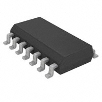
M74HC132RM13TR

M74HC132RM13TR

  • 厂商:

    STMICROELECTRONICS(意法半导体)

  • 封装:

  • 描述:

    M74HC132RM13TR - QUAD 2-INPUT SCHMITT NAND GATE - STMicroelectronics

  • 详情介绍
  • 数据手册
  • 价格&库存
M74HC132RM13TR 数据手册
M74HC132 QUAD 2-INPUT SCHMITT NAND GATE s s s s s s s HIGH SPEED: tPD = 11ns (TYP.) at VCC = 6V LOW POWER DISSIPATION: ICC = 1µA(MAX.) at TA=25°C HIGH NOISE IMMUNITY: VH(TYP.) = 0.9 V AT VCC = 5 V SYMMETRICAL OUTPUT IMPEDANCE: |IOH| = IOL = 4mA (MIN) BALANCED PROPAGATION DELAYS: tPLH ≅ tPHL WIDE OPERATING VOLTAGE RANGE: VCC (OPR) = 2V to 6V PIN AND FUNCTION COMPATIBLE WITH 74 SERIES 132 DIP SOP TSSOP ORDER CODES PACKAGE DIP SOP TSSOP TUBE M74HC132B1R M74HC132M1R T&R M74HC132RM13TR M74HC132TTR DESCRIPTION The M74HC132 is an high speed CMOS QUAD 2-INPUT SCHMITT NAND GATE fabricated with silicon gate C2MOS technology. Pin configuration and function are identical to those of the M74HC00. The hysteresis characteristics (around 20% Vcc ) of all inputs allow slowly changing input signals to be transformed into sharply defined jitter-free output signals. All inputs are equipped with protection circuits against static discharge and transient excess voltage. PIN CONNECTION AND IEC LOGIC SYMBOLS March 2002 1/9 M74HC132 INPUT AND OUTPUT EQUIVALENT CIRCUIT PIN DESCRIPTION PIN No 1, 4, 9, 12 2, 5, 10, 13 3, 6, 8, 11 7 14 SYMBOL 1A to 4A 1B to 4B 1Y to 4Y GND VCC NAME AND FUNCTION Data Inputs Data Inputs Data Outputs Ground (0V) Positive Supply Voltage TRUTH TABLE A L L H H B L H L H Y H H H L ABSOLUTE MAXIMUM RATINGS Symbol VCC VI VO IIK IOK IO PD Supply Voltage DC Input Voltage DC Output Voltage DC Input Diode Current DC Output Diode Current DC Output Current Power Dissipation DIP SOP TSSOP Parameter Value -0.5 to +7 -0.5 to VCC + 0.5 -0.5 to VCC + 0.5 ± 20 ± 20 ± 25 ± 50 750(*) 500(*) 450(*) -65 to +150 300 Unit V V V mA mA mA mA mW mW mW °C °C ICC or IGND DC VCC or Ground Current Tstg TL Storage Temperature Lead Temperature (10 sec) Absolute Maximum Ratings are those values beyond which damage to the device may occur. Functional operation under these conditions is not implied (*) Power difssipation at 65 °C. Derating from 65°C to 125°C: DIP Package -10mW/°C; SO Package -7mW/°C; TSSOP Package -6.1mW/°C RECOMMENDED OPERATING CONDITIONS Symbol VCC VI VO Top Supply Voltage Input Voltage Output Voltage Operating Temperature Parameter Value 2 to 6 0 to VCC 0 to VCC -55 to 125 Unit V V V °C 2/9 M74HC132 DC SPECIFICATIONS Test Condition Symbol Parameter VCC (V) 2.0 4.5 6.0 2.0 4.5 6.0 2.0 4.5 6.0 2.0 4.5 6.0 4.5 6.0 VOL Low Level Output Voltage 2.0 4.5 6.0 4.5 6.0 II ICC Input Leakage Current Quiescent Supply Current 6.0 6.0 IO=-20 µA IO=-20 µA IO=-20 µA IO=-4.0 mA IO=-5.2 mA IO=-20 µA IO=-20 µA IO=-20 µA IO=-4.0 mA IO=-5.2 mA VI = VCC or GND VI = VCC or GND TA = 25°C Min. 1.0 2.3 3.0 0.3 1.13 1.5 0.3 0.6 0.8 1.9 4.4 5.9 4.18 5.68 Typ. 1.25 2.7 3.5 0.65 1.6 2.3 0.6 1.1 1.2 2.0 4.5 6.0 4.31 5.8 0.0 0.0 0.0 0.17 0.18 0.1 0.1 0.1 0.26 0.26 ± 0.1 1 Max. 1.5 3.15 4.2 0.9 2.0 2.6 1.0 1.4 1.4 Value -40 to 85°C Min. 1.0 2.3 3.0 0.3 1.13 1.5 0.3 0.6 0.8 1.9 4.4 5.9 4.13 5.63 0.1 0.1 0.1 0.33 0.33 ±1 10 Max. 1.5 3.15 4.2 0.9 2.0 2.6 1.0 1.4 1.7 -55 to 125°C Min. 1.0 2.3 3.0 0.3 1.13 1.5 0.3 0.6 0.8 1.9 4.4 5.9 4.10 5.60 0.1 0.1 0.1 0.40 0.40 ±1 20 µA µA V V Max. 1.5 3.15 4.2 0.9 2.0 2.6 1.0 1.4 1.7 V Unit VP High Level Threshold Voltage Low Level Threshold Voltage Hysteresis Voltage VN V VH V VOH High Level Output Voltage AC ELECTRICAL CHARACTERISTICS (CL = 50 pF, Input tr = tf = 6ns) Test Condition Symbol Parameter VCC (V) 2.0 4.5 6.0 2.0 4.5 6.0 TA = 25°C Min. Typ. 30 8 7 52 13 11 Max. 75 15 13 105 21 18 Value -40 to 85°C Min. Max. 95 19 16 130 26 22 -55 to 125°C Min. Max. 110 22 19 160 32 27 ns Unit tTLH tTHL Output Transition Time tPLH tPHL Propagation Delay Time ns 3/9 M74HC132 CAPACITIVE CHARACTERISTICS Test Condition Symbol Parameter VCC (V) 5.0 5.0 TA = 25°C Min. Typ. 5 29 Max. 10 Value -40 to 85°C Min. Max. 10 -55 to 125°C Min. Max. 10 pF pF Unit CIN CPD Input Capacitance Power Dissipation Capacitance (note 1) 1) CPD is defined as the value of the IC’s internal equivalent capacitance which is calculated from the operating current consumption without load. (Refer to Test Circuit). Average operating current can be obtained by the following equation. ICC(opr) = CPD x VCC x fIN + ICC/4 (per gate) TEST CIRCUIT CL = 50pF or equivalent (includes jig and probe capacitance) RT = ZOUT of pulse generator (typically 50Ω) 4/9 M74HC132 WAVEFORM : PROPAGATION DELAY TIMES (f=1MHz; 50% duty cycle) 5/9 M74HC132 Plastic DIP-14 MECHANICAL DATA mm. DIM. MIN. a1 B b b1 D E e e3 F I L Z 1.27 3.3 2.54 0.050 8.5 2.54 15.24 7.1 5.1 0.130 0.100 0.51 1.39 0.5 0.25 20 0.335 0.100 0.600 0.280 0.201 1.65 TYP MAX. MIN. 0.020 0.055 0.020 0.010 0.787 0.065 TYP. MAX. inch P001A 6/9 M74HC132 SO-14 MECHANICAL DATA DIM. A a1 a2 b b1 C c1 D E e e3 F G L M S 3.8 4.6 0.5 8.55 5.8 1.27 7.62 4.0 5.3 1.27 0.68 8° (max.) 0.149 0.181 0.019 8.75 6.2 0.35 0.19 0.5 45° (typ.) 0.336 0.228 0.050 0.300 0.157 0.208 0.050 0.026 0.344 0.244 0.1 mm. MIN. TYP MAX. 1.75 0.2 1.65 0.46 0.25 0.013 0.007 0.019 0.003 MIN. inch TYP. MAX. 0.068 0.007 0.064 0.018 0.010 PO13G 7/9 M74HC132 TSSOP14 MECHANICAL DATA mm. DIM. MIN. A A1 A2 b c D E E1 e K L 0° 0.45 0.60 0.05 0.8 0.19 0.09 4.9 6.2 4.3 5 6.4 4.4 0.65 BSC 8° 0.75 0° 0.018 0.024 1 TYP MAX. 1.2 0.15 1.05 0.30 0.20 5.1 6.6 4.48 0.002 0.031 0.007 0.004 0.193 0.244 0.169 0.197 0.252 0.173 0.0256 BSC 8° 0.030 0.004 0.039 MIN. TYP. MAX. 0.047 0.006 0.041 0.012 0.0089 0.201 0.260 0.176 inch A A2 A1 b e K c L E D E1 PIN 1 IDENTIFICATION 1 0080337D 8/9 M74HC132 Information furnished is believed to be accurate and reliable. However, STMicroelectronics assumes no responsibility for the consequences of use of such information nor for any infringement of patents or other rights of third parties which may result from its use. No license is granted by implication or otherwise under any patent or patent rights of STMicroelectronics. Specifications mentioned in this publication are subject to change without notice. This publication supersedes and replaces all information previously supplied. STMicroelectronics products are not authorized for use as critical components in life support devices or systems without express written approval of STMicroelectronics. © The ST logo is a registered trademark of STMicroelectronics © 2002 STMicroelectronics - Printed in Italy - All Rights Reserved STMicroelectronics GROUP OF COMPANIES Australia - Brazil - Canada - China - Finland - France - Germany - Hong Kong - India - Israel - Italy - Japan - Malaysia - Malta - Morocco Singapore - Spain - Sweden - Switzerland - United Kingdom - United States. © http://www.st.com 9/9
M74HC132RM13TR
1. 物料型号: - DIP封装:M74HC132B1R - SOP封装:M74HC132M1R - SOP封装(卷带与轴向):M74HC132RM13TR - TSSOP封装:无特定型号,但有M74HC132TTR

2. 器件简介: - M74HC132是一款高速CMOS四2输入施密特触发反相器,采用2硅门C2MOS技术制造。所有输入都配备了防静电放电和瞬态过电压的保护电路。引脚配置和功能与M74HC00相同。所有输入的滞后特性(大约20% Vcc)允许慢变化的输入信号被转换成清晰无抖动的输出信号。

3. 引脚分配: - 1, 4, 9, 12:1A至4A(数据输入) - 2, 5, 10, 13:1B至4B(数据输入) - 3, 6, 8, 11:1Y至4Y(数据输出) - 7:GND(地,0V) - 14:Vcc(正电源电压)

4. 参数特性: - 工作电压范围:2V至6V - 输入电压:0至Vcc - 输出电压:0至Vcc - 工作温度:-55至125°C

5. 功能详解: - M74HC132的输入具有滞后特性,能够将缓慢变化的输入信号转换为清晰无抖动的输出信号。此外,该器件还具有高速(典型值11ns的传播延迟)和低功耗(25°C时最大1μA的功耗)的特点。

6. 应用信息: - 该器件适用于需要高速和低功耗施密特触发反相器的数字逻辑应用。

7. 封装信息: - 提供了DIP、SOP和TSSOP三种封装形式的详细机械尺寸数据。
M74HC132RM13TR 价格&库存

很抱歉,暂时无法提供与“M74HC132RM13TR”相匹配的价格&库存,您可以联系我们找货

免费人工找货