物料型号:
- DIP封装:M74HC164B1R
- SOP封装:M74HC164M1R
- SOP封装,卷带与轴向(T&R):M74HC164RM13TR
- TSSOP封装:无特定型号
- TSSOP封装,卷带与轴向(T&R):M74HC164TTR
器件简介:
M74HC164是一款高速CMOS 8位串行入并行出(SIPO)移位寄存器,采用硅门CMOS技术制造。该器件具有串行数据输入和8个阶段的输出。数据通过两个输入端(A或B)之一串行输入,任一输入端也可以用作通过另一输入端输入数据的高电平使能端。未使用的输入端必须为高电平,或两个输入端连接在一起。每个低至高的时钟输入转换将数据右移一位,并将两个数据输入的逻辑NAND(A X B)输入到QA,即在上升时钟边沿之前的数据。清除输入端的低电平会覆盖所有其他输入,异步清除寄存器,将所有Q输出端强制为低电平。所有输入端都配备了防静电和瞬态过电压的保护电路。
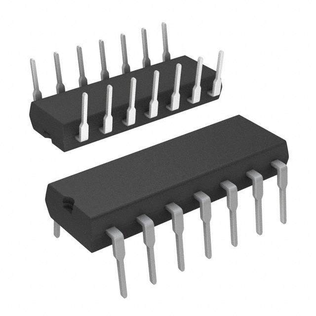
引脚分配:
- 1, 2脚:A, B(数据输入)
- 3, 4, 5, 6, 10, 11, 12, 13脚:QA至QH(输出)
- 8脚:时钟输入(CLOCK,低至高边沿触发)
- 9脚:清除(CLEAR,主复位输入)
- 7脚:地(GND,0V)
- 14脚:供电电压(Vcc,正供电电压)
参数特性:
- 最高频率:fMAX = 62MHz(典型值,Vcc=6V)
- 最大功耗:Icc=4μA(最大值,Ta=25°C)
- 高噪声免疫力:Vnih=Vnil=28%Vcc(最小值)
- 对称的输出阻抗:|Ioh|=Iol=4mA(最小值)
- 平衡的传播延迟:tplh≈tphl
- 宽工作电压范围:Vcc(op)=2V至6V
功能详解:
M74HC164具有两个数据输入端(A和B),可以通过任一输入端串行输入数据,并且每个上升时钟沿将数据右移一位。数据输入为两个输入端的逻辑NAND(A X B)。清除输入端的低电平会异步清除寄存器,将所有输出Q端强制为低电平。
应用信息:
M74HC164由于其高速和低功耗特性,适用于需要高速数据传输和存储的应用,如数字信号处理、数据缓冲、数据分配等。
封装信息:
M74HC164提供多种封装选项,包括DIP、SOP和TSSOP,以适应不同的应用和空间要求。