M74HC294
PROGRAMMABLE DIVIDER/TIMER
■
■
HIGH SPEED :
fMAX = 75 MHz (TYP.) at VCC = 6V
LOW POWER DISSIPATION:
ICC =4µA(MAX.) at TA=25°C
HIGH NOISE IMMUNITY:
VNIH = V NIL = 28 % VCC (MIN.)
SYMMETRICAL OUTPUT IMPEDANCE:
|IOH| = IOL = 4mA (MIN)
BALANCED PROPAGATION DELAYS:
tPLH ≅ tPHL
WIDE OPERATING VOLTAGE RANGE:
VCC (OPR) = 2V to 6V
PIN AND FUNCTION COMPATIBLE WITH
74 SERIES 294
)
s
(
t
c
u
d
o
)
r
s
(
P
t
c
e
t
u
e
d
l
o
o
r
s
P
b
e
O
t
e
l
)
o
s
(
s
t
b
c
u
O
d
o
)
r
s
P
(
t
c
e
t
u
e
l
d
o
o
r
s
P
b
O
e
t
e
l
o
s
b
O
■
■
■
■
■
DESCRIPTION
The M74HC294 is an high speed CMOS
PROGRAMMABLE DIVIDER/TIMER fabricated
with silicon gate C2MOS technology.
This device is a programmable frequency divider
and has two clock inputs, either one may be used
for clock gating. (see the function table).
The M74HC294 can divide from 22 to 215. This
device feature an active-low clear input to initialize
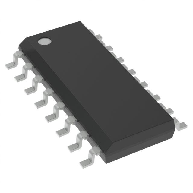
DIP
SOP
TSSOP
ORDER CODES
PACKAGE
TUBE
DIP
SOP
TSSOP
M74HC294B1R
M74HC294M1R
T&R
M74HC294RM13TR
M74HC294TTR
the state of all flip-flops. To facilitate incoming
inspection, test points (TP) are provided. All
inputs are equipped with protection circuits
against static discharge and transient excess
voltage.
This device has Q output with "Totem Pole"
configuration and test point TP with "Open Drain"
output configuration.
PIN CONNECTION AND IEC LOGIC SYMBOLS
August 2001
1/11
�M74HC294
INPUT AND OUTPUT EQUIVALENT CIRCUIT
(TOTEM POLE OUTPUT)
INPUT AND OUTPUT EQUIVALENT CIRCUIT
(OPEN DRAIN OUTPUT)
)
s
(
t
c
u
d
o
)
r
s
(
P
t
c
e
t
u
e
d
l
o
o
r
s
P
b
e
O
t
e
l
)
o
s
(
s
t
b
c
u
O
d
o
)
r
s
P
(
t
c
e
t
u
e
l
d
o
o
r
s
P
b
O
e
t
e
l
o
s
b
O
PIN DESCRIPTION
PIN No
SYMBOL
4, 5
1, 2, 14, 15
3
11
7
8
16
CLK1, CLK2
A to E
TP
CLR
Q
GND
Vcc
NAME AND FUNCTION
Input Clock
Program Inputs
Test Point Outputs
Clear (Active LOW)
Output
Ground (0V)
Positive Supply Voltage
TRUTH TABLE
CLR
CLK1
CLK2
Q OUTPUT MODE
L
X
X
CLEARED TO L
H
2/11
L
H
L
H
H
H
X
X
H
UP COUNT
NO CHANGE
�M74HC294
LOGIC DIAGRAM
)
s
(
t
c
u
d
o
)
r
s
(
P
t
c
e
t
u
e
d
l
o
o
r
s
P
b
e
O
t
e
l
)
o
s
(
s
t
b
c
u
O
d
o
)
r
s
P
(
t
c
e
t
u
e
l
d
o
o
r
s
P
b
O
e
t
e
l
o
s
b
O
This logic diagram has not be used to estimate propagation delays
3/11
�M74HC294
FUNCTIONAL TABLE
FREQUENCY DIVISION
PROGRAMMING INPUTS
Q
TP
D
C
B
A
BINARY
L
L
L
L
L
L
L
H
Inhibit
Inhibit
DECIMAL BINARY
DECIMAL
L
L
H
L
22
4 29
512
29
512
9
512
Inhibit Inhibit
Inhibit Inhibit
Inhibit
Inhibit
L
L
H
H
23
L
H
L
L
4
2
16 2
L
H
L
H
25
32 29
L
6
2
9
128 Disabled Low
L
H
H
8
L
H
H
H
H
L
L
L
28
256 22
H
9
512 23
H
L
L
2
10
4
H
L
H
L
H
L
H
H
2
2.048 2
H
H
L
L
212
4.096 26
11
H
H
L
H
213
H
H
H
L
214
H
H
H
H
215
od
Supply Voltage
VI
DC Input Voltage
VO
DC Output Voltage
ete
IIK
Pr
l
o
s
16.384
28
e
t
le
32.768 29
o
s
b
O
-
Pr
Pr
uc
od
512
4
)
s
t(
8
16
32
64
128
256
512
Value
Unit
-0.5 to +7
V
-0.5 to VCC + 0.5
-0.5 to VCC + 0.5
V
V
± 20
mA
± 20
mA
DC Output Current
± 25
mA
± 50
mA
d
o
r
P
e
t
e
l
o
Tstg
Storage Temperature
TL
Lead Temperature (10 sec)
s
b
O
(s)
t
c
u
ICC or IGND DC VCC or Ground Current
PD
Power Dissipation
b
O
)
(s
b
O
8.192
27
u
d
o
512
DC Output Diode Current
DC Input Diode Current
IO
so
Parameter
VCC
e
t
e
l
5
t
c
u
Symbol
IOK
1.024 2
2
ABSOLUTE MAXIMUM RATINGS
ct
64 2
27
(s)
500(*)
mW
-65 to +150
°C
300
°C
Absolute Maximum Ratings are those values beyond which damage to the device may occur. Functional operation under these conditions is
not implied
(*) 500mW at 65 °C; derate to 300mW by 10mW/°C from 65°C to 85°C
4/11
�M74HC294
RECOMMENDED OPERATING CONDITIONS
Symbol
VCC
Parameter
Value
Supply Voltage
VI
Input Voltage
VO
Output Voltage
Top
Operating Temperature
Input Rise and Fall Time
tr, tf
Unit
2 to 6
V
0 to VCC
V
0 to VCC
V
-55 to 125
°C
VCC = 2.0V
0 to 1000
ns
VCC = 4.5V
0 to 500
ns
VCC = 6.0V
0 to 400
ns
)
s
(
t
c
u
d
o
)
r
s
(
P
t
c
e
t
u
e
d
l
o
o
r
s
P
b
e
O
t
e
l
)
o
s
(
s
t
b
c
u
O
d
o
)
r
s
P
(
t
c
e
t
u
e
l
d
o
o
r
s
P
b
O
e
t
e
l
o
s
b
O
DC SPECIFICATIONS
Test Condition
Symbol
VIH
VIL
VOH
VOL
VOL
II
ICC
Parameter
High Level Input
Voltage
Low Level Input
Voltage
High Level Output
Voltage (Q)
Low Level Output
Voltage (Q)
Low Level Output
Voltage (TP)
Input Leakage
Current
Quiescent Supply
Current
Value
TA = 25°C
VCC
(V)
Min.
2.0
4.5
6.0
2.0
4.5
6.0
Typ.
Max.
1.5
3.15
4.2
-40 to 85°C
-55 to 125°C
Min.
Min.
Max.
1.5
3.15
4.2
0.5
1.35
1.8
Max.
1.5
3.15
4.2
0.5
1.35
1.8
0.5
1.35
1.8
2.0
IO=-20 µA
1.9
2.0
1.9
1.9
4.5
IO=-20 µA
4.4
4.5
4.4
4.4
6.0
IO=-20 µA
5.9
6.0
5.9
5.9
4.5
IO=-4.0 mA
4.18
4.31
4.13
4.10
6.0
IO=-5.2 mA
5.68
2.0
IO=20 µA
0.0
0.1
0.1
0.1
4.5
IO=20 µA
0.0
0.1
0.1
0.1
6.0
IO=20 µA
0.0
0.1
0.1
0.1
4.5
IO=4.0 mA
0.17
0.26
0.33
0.40
6.0
IO=5.2 mA
0.18
0.26
0.33
0.40
2.0
IO=20 µA
0.0
0.1
0.1
0.1
4.5
IO=20 µA
0.0
0.1
0.1
0.1
5.8
5.63
Unit
V
V
V
5.60
V
6.0
IO=20 µA
0.0
0.1
0.1
0.1
4.5
IO=1.0 mA
0.17
0.26
0.33
0.40
6.0
IO=1.3 mA
0.18
0.26
0.33
0.40
6.0
VI = VCC or GND
± 0.1
±1
±1
µA
6.0
VI = VCC or GND
4
40
80
µA
V
5/11
�M74HC294
AC ELECTRICAL CHARACTERISTICS (CL = 50 pF, Input tr = tf = 6ns)
Test Condition
Symbol
Parameter
tTLH tTHL Output Transition
Time (Q)
tTLH tTHL Output Transition
Time (TP)
Value
TA = 25°C
VCC
(V)
Min.
2.0
4.5
6.0
2.0
4.5
6.0
2.0
4.5
6.0
2.0
4.5
6.0
2.0
4.5
6.0
2.0
4.5
6.0
2.0
4.5
6.0
2.0
4.5
6.0
Typ.
Max.
30
8
7
116
29
25
145
43
37
110
34
29
20
64
75
40
8
7
40
10
9
75
15
13
225
45
38
330
66
56
260
52
44
-40 to 85°C
-55 to 125°C
Min.
Min.
Max.
95
19
16
280
56
48
415
83
71
325
65
55
Unit
Max.
110
22
19
340
68
57
ns
ns
)
s
(
t
c
u
d
o
)
r
s
(
P
t
c
e
t
u
e
d
l
o
o
r
s
P
b
e
O
t
e
l
)
o
s
(
s
t
b
c
u
O
d
o
)
r
s
P
(
t
c
e
t
u
e
l
d
o
o
r
s
P
b
O
e
t
e
l
o
s
b
O
tPLH tPHL Propagation Delay
Time
(CLK - Q)
tPHL
fMAX
Propagation Delay
Time
(CLR - Q)
Maximum Clock
Frequency
tW(L)
tW(H)
Minimum Pulse
Width (CLK)
tW(L)
Minimum Pulse
Width (CLR)
tREM
Minimum Removal
Time
6.0
32
38
5
26
31
75
15
13
100
20
17
0
0
0
15
84
390
78
66
4
21
25
95
19
16
125
25
21
0
0
0
ns
ns
MHz
110
22
20
150
30
26
0
0
0
ns
ns
ns
CAPACITIVE CHARACTERISTICS
Test Condition
Symbol
Parameter
VCC
(V)
Value
TA = 25°C
Typ.
Max.
CIN
Input Capacitance
5.0
Min.
5
10
CPD
Power Dissipation
Capacitance (note
1)
5.0
23
-40 to 85°C
-55 to 125°C
Min.
Min.
Max.
10
Unit
Max.
10
pF
pF
1) CPD is defined as the value of the IC’s internal equivalent capacitance which is calculated from the operating current consumption without
load. (Refer to Test Circuit). Average operating current can be obtained by the following equation. ICC(opr) = CPD x VCC x fIN + ICC
6/11
�M74HC294
TEST CIRCUIT
)
s
(
t
c
u
d
o
)
r
s
(
P
t
c
e
t
u
e
d
l
o
o
r
s
P
b
e
O
t
e
l
)
o
s
(
s
t
b
c
u
O
d
o
)
r
s
P
(
t
c
e
t
u
e
l
d
o
o
r
s
P
b
O
e
t
e
l
o
s
b
O
CL = 50pF or equivalent (includes jig and probe capacitance)
RT = ZOUT of pulse generator (typically 50Ω)
SWITCHING CHARACTERISTICS TEST WAVEFORM : (f=1MHz; 50% duty cycle)
7/11
�M74HC294
Plastic DIP-16 (0.25) MECHANICAL DATA
mm.
inch
DIM.
MIN.
a1
0.51
B
0.77
b
TYP
MAX.
MIN.
TYP.
MAX.
0.020
1.65
0.5
0.030
0.065
0.020
)
s
(
t
c
u
d
o
)
r
s
(
P
t
c
e
t
u
e
d
l
o
o
r
s
P
b
e
O
t
e
l
)
o
s
(
s
t
b
c
u
O
d
o
)
r
s
P
(
t
c
e
t
u
e
l
d
o
o
r
s
P
b
O
e
t
e
l
o
s
b
O
b1
0.25
D
0.010
20
0.787
E
8.5
0.335
e
2.54
0.100
e3
17.78
0.700
F
7.1
0.280
I
5.1
0.201
L
Z
3.3
0.130
1.27
0.050
P001C
8/11
�M74HC294
SO-16 MECHANICAL DATA
DIM.
mm.
MIN.
TYP
A
a1
MAX.
MIN.
TYP.
1.75
0.1
0.003
0.007
1.65
0.35
MAX.
0.068
0.2
a2
b
inch
0.064
0.46
0.013
0.018
)
s
(
t
c
u
d
o
)
r
s
(
P
t
c
e
t
u
e
d
l
o
o
r
s
P
b
e
O
t
e
l
)
o
s
(
s
t
b
c
u
O
d
o
)
r
s
P
(
t
c
e
t
u
e
l
d
o
o
r
s
P
b
O
e
t
e
l
o
s
b
O
b1
0.19
C
0.25
0.007
0.5
0.010
0.019
c1
45° (typ.)
D
9.8
10
0.385
0.393
E
5.8
6.2
0.228
0.244
e
1.27
0.050
e3
8.89
0.350
F
3.8
4.0
0.149
0.157
G
4.6
5.3
0.181
0.208
L
0.5
1.27
0.019
0.050
M
S
0.62
0.024
8° (max.)
PO13H
9/11
�M74HC294
TSSOP16 MECHANICAL DATA
mm.
inch
DIM.
MIN.
TYP
A
MAX.
MIN.
TYP.
MAX.
1.2
A1
0.05
A2
0.8
b
0.047
0.15
0.002
0.004
0.006
1.05
0.031
0.039
0.041
0.19
0.30
0.007
0.012
c
0.09
0.20
0.004
0.0089
D
4.9
5
5.1
0.193
0.197
0.201
E
6.2
6.4
6.6
0.244
0.252
0.260
E1
4.3
4.4
4.48
0.169
0.173
0.176
1
)
s
(
t
c
u
d
o
)
r
s
(
P
t
c
e
t
u
e
d
l
o
o
r
s
P
b
e
O
t
e
l
)
o
s
(
s
t
b
c
u
O
d
o
)
r
s
P
(
t
c
e
t
u
e
l
d
o
o
r
s
P
b
O
e
t
e
l
o
s
b
O
e
0.65 BSC
K
0°
L
0.45
A
0.60
0.0256 BSC
8°
0°
0.75
0.018
8°
0.024
0.030
A2
A1
b
e
K
c
L
E
D
E1
PIN 1 IDENTIFICATION
1
0080338D
10/11
�M74HC294
)
s
(
t
c
u
d
o
)
r
s
(
P
t
c
e
t
u
e
d
l
o
o
r
s
P
b
e
O
t
e
l
)
o
s
(
s
t
b
c
u
O
d
o
)
r
s
P
(
t
c
e
t
u
e
l
d
o
o
r
s
P
b
O
e
t
e
l
o
s
b
O
Information furnished is believed to be accurate and reliable. However, STMicroelectronics assumes no responsibility for the
consequences of use of such information nor for any infringement of patents or other rights of third parties which may result from
its use. No license is granted by implication or otherwise under any patent or patent rights of STMicroelectronics. Specifications
mentioned in this publication are subject to change without notice. This publication supersedes and replaces all information
previously supplied. STMicroelectronics products are not authorized for use as critical components in life support devices or
systems without express written approval of STMicroelectronics.
© The ST logo is a registered trademark of STMicroelectronics
© 2001 STMicroelectronics - Printed in Italy - All Rights Reserved
STMicroelectronics GROUP OF COMPANIES
Australia - Brazil - China - Finland - France - Germany - Hong Kong - India - Italy - Japan - Malaysia - Malta - Morocco
Singapore - Spain - Sweden - Switzerland - United Kingdom
© http://www.st.com
11/11
�
很抱歉,暂时无法提供与“M74HC294RM13TR”相匹配的价格&库存,您可以联系我们找货
免费人工找货