M74HC377B1R

M74HC377B1R

  • 厂商:

    STMICROELECTRONICS(意法半导体)

  • 封装:

    DIP20

  • 描述:

    IC FF D-TYPE SNGL 8BIT 20DIP

  • 详情介绍
  • 数据手册
  • 价格&库存
M74HC377B1R 数据手册
M74HC377 OCTAL D TYPE FLIP FLOP s s s s s s s HIGH SPEED : fMAX = 66 MHz (TYP.) at VCC = 6V LOW POWER DISSIPATION: ICC =4µA(MAX.) at TA=25°C HIGH NOISE IMMUNITY: VNIH = V NIL = 28 % VCC (MIN.) SYMMETRICAL OUTPUT IMPEDANCE: |IOH| = IOL = 4mA (MIN) BALANCED PROPAGATION DELAYS: tPLH ≅ tPHL WIDE OPERATING VOLTAGE RANGE: VCC (OPR) = 2V to 6V PIN AND FUNCTION COMPATIBLE WITH 74 SERIES 377 DIP SOP TSSOP ORDER CODES PACKAGE DIP SOP TSSOP TUBE M74HC377B1R M74HC377M1R T&R M74HC377RM13TR M74HC377TTR DESCRIPTION The M74HC377 is an high speed CMOS OCTAL D TYPE FLIP FLOP fabricated with silicon gate C2MOS technology. Information at the D inputs meeting the setup time requirements is transferred to the Q outputs on the positive going edge of the clock pulse if the enable input G is low. Clock triggering occurs at a particular voltage level and is not directly related to the transition time of the positive going pulse. When the clock input is at either the high or low level, the D input signal has no effect at the output. All inputs are equipped with protection circuits against static discharge and transient excess voltage. PIN CONNECTION AND IEC LOGIC SYMBOLS July 2001 1/11 M74HC377 INPUT AND OUTPUT EQUIVALENT CIRCUIT PIN DESCRIPTION PIN No 1 2, 5, 6, 9, 12, 15, 16, 19 3, 4, 7, 8, 13, 14, 17, 18 11 10 20 SYMBOL G 1Q to 8Q 1D to 8D CLOCK GND Vcc NAME AND FUNCTION Data Enable Input (Active LOW) Flip Flop Outputs Data Inputs Clock Input (LOW to HIGH, Edge Triggered) Ground (0V) Positive Supply Voltage TRUTH TABLE INPUTS G H L L X X : Don’t Care OUTPUTS DATA X L H X Q NO CHANGE L H NO CHANGE CLOCK X LOGIC DIAGRAM This logic diagram has not be used to estimate propagation delays 2/11 M74HC377 ABSOLUTE MAXIMUM RATINGS Symbol VCC VI VO IIK IOK IO PD Tstg TL Supply Voltage DC Input Voltage DC Output Voltage DC Input Diode Current DC Output Diode Current DC Output Current Power Dissipation Storage Temperature Lead Temperature (10 sec) Parameter Value -0.5 to +7 -0.5 to VCC + 0.5 -0.5 to VCC + 0.5 ± 20 ± 20 ± 25 ± 50 500(*) -65 to +150 300 Unit V V V mA mA mA mA mW °C °C ICC or IGND DC VCC or Ground Current Absolute Maximum Ratings are those values beyond which damage to the device may occur. Functional operation under these conditions is not implied (*) 500mW at 65 °C; derate to 300mW by 10mW/°C from 65°C to 85°C RECOMMENDED OPERATING CONDITIONS Symbol VCC VI VO Top tr, tf Supply Voltage Input Voltage Output Voltage Operating Temperature Input Rise and Fall Time VCC = 2.0V VCC = 4.5V VCC = 6.0V Parameter Value 2 to 6 0 to VCC 0 to VCC -55 to 125 0 to 1000 0 to 500 0 to 400 Unit V V V °C ns ns ns 3/11 M74HC377 DC SPECIFICATIONS Test Condition Symbol Parameter VCC (V) 2.0 4.5 6.0 2.0 4.5 6.0 2.0 4.5 6.0 4.5 6.0 VOL Low Level Output Voltage 2.0 4.5 6.0 4.5 6.0 II ICC Input Leakage Current Quiescent Supply Current 6.0 6.0 IO=-20 µA IO=-20 µA IO=-20 µA IO=-4.0 mA IO=-5.2 mA IO=20 µA IO=20 µA IO=20 µA IO=4.0 mA IO=5.2 mA VI = VCC or GND VI = VCC or GND TA = 25°C Min. 1.5 3.15 4.2 0.5 1.35 1.8 1.9 4.4 5.9 4.18 5.68 2.0 4.5 6.0 4.31 5.8 0.0 0.0 0.0 0.17 0.18 0.1 0.1 0.1 0.26 0.26 ± 0.1 4 1.9 4.4 5.9 4.13 5.63 0.1 0.1 0.1 0.33 0.33 ±1 40 Typ. Max. Value -40 to 85°C Min. 1.5 3.15 4.2 0.5 1.35 1.8 1.9 4.4 5.9 4.10 5.60 0.1 0.1 0.1 0.40 0.40 ±1 80 µA µA V V Max. -55 to 125°C Min. 1.5 3.15 4.2 0.5 1.35 1.8 Max. V Unit VIH High Level Input Voltage Low Level Input Voltage High Level Output Voltage VIL V VOH 4/11 M74HC377 AC ELECTRICAL CHARACTERISTICS (CL = 50 pF, Input tr = tf = 6ns) Test Condition Symbol Parameter VCC (V) 2.0 4.5 6.0 2.0 4.5 6.0 2.0 4.5 6.0 2.0 4.5 6.0 2.0 4.5 6.0 2.0 4.5 6.0 2.0 4.5 6.0 TA = 25°C Min. Typ. 30 8 7 57 17 13 14 56 66 24 6 5 24 6 5 30 8 6 Max. 75 15 13 140 28 24 5.8 29 34 75 15 13 75 15 13 75 15 13 0 0 0 95 19 16 95 19 16 95 19 16 0 0 0 Value -40 to 85°C Min. Max. 95 19 16 175 35 30 4.8 24 28 115 23 20 115 23 20 115 23 20 0 0 0 -55 to 125°C Min. Max. 110 22 19 210 42 36 ns Unit tTLH tTHL Output Transition Time tPLH tPHL Propagation Delay Time (CLOCK - Q) fMAX Maximum Clock Frequency Minimum Pulse Width (CLOCK) Minimum Set-up Time (D - CK) Minimum Set-up Time (G - CK) Minimum Hold Time ns 7.2 36 42 MHz tW(H) tW(L) ts ns ns ts ns th ns CAPACITIVE CHARACTERISTICS Test Condition Symbol Parameter VCC (V) 5.0 5.0 TA = 25°C Min. Typ. 5 34 Max. 10 Value -40 to 85°C Min. Max. 10 -55 to 125°C Min. Max. 10 pF pF Unit CIN CPD Input Capacitance Power Dissipation Capacitance (note 1) 1) CPD is defined as the value of the IC’s internal equivalent capacitance which is calculated from the operating current consumption without load. (Refer to Test Circuit). Average operating current can be obtained by the following equation. ICC(opr) = CPD x VCC x fIN + ICC 5/11 M74HC377 TEST CIRCUIT CL = 50pF or equivalent (includes jig and probe capacitance) RT = ZOUT of pulse generator (typically 50Ω) WAVEFORM 1: PROPAGATION DELAY TIME, MINIMUM PULSE WIDTH (CK), SETUP AND HOLD TIME (D TO CK) (f=1MHz; 50% duty cycle) 6/11 M74HC377 WAVEFORM 2 :CK MAXIMUM FREQUENCY (f=1MHz; 50% duty cycle) W AVEFORM 3 : SETUP AND HOLD TIME (G TO CK) (f=1MHz; 50% duty cycle) 7/11 M74HC377 Plastic DIP-20 (0.25) MECHANICAL DATA mm. DIM. MIN. a1 B b b1 D E e e3 F I L Z 3.3 1.34 8.5 2.54 22.86 7.1 3.93 0.130 0.053 0.254 1.39 0.45 0.25 25.4 0.335 0.100 0.900 0.280 0.155 1.65 TYP MAX. MIN. 0.010 0.055 0.018 0.010 1.000 0.065 TYP. MAX. inch P001J 8/11 M74HC377 SO-20 MECHANICAL DATA mm. DIM. MIN. A a1 a2 b b1 C c1 D E e e3 F L M S 7.40 0.50 12.60 10.00 1.27 11.43 7.60 1.27 0.75 8° (max.) 0.291 0.020 13.00 10.65 0.35 0.23 0.5 45° (typ.) 0.496 0.393 0.050 0.450 0.300 0.050 0.029 0.512 0.419 0.1 TYP MAX. 2.65 0.2 2.45 0.49 0.32 0.014 0.009 0.020 0.004 MIN. TYP. MAX. 0.104 0.008 0.096 0.019 0.012 inch PO13L 9/11 M74HC377 TSSOP20 MECHANICAL DATA mm. DIM. MIN. A A1 A2 b c D E E1 e K L 0° 0.45 0.60 0.05 0.8 0.19 0.09 6.4 6.2 4.3 6.5 6.4 4.4 0.65 BSC 8° 0.75 0° 0.018 0.024 1 TYP MAX. 1.2 0.15 1.05 0.30 0.20 6.6 6.6 4.48 0.002 0.031 0.007 0.004 0.252 0.244 0.169 0.256 0.252 0.173 0.0256 BSC 8° 0.030 0.004 0.039 MIN. TYP. MAX. 0.047 0.006 0.041 0.012 0.0089 0.260 0.260 0.176 inch A A2 A1 b e K c L E D E1 PIN 1 IDENTIFICATION 1 0087225C 10/11 M74HC377 Information furnished is believed to be accurate and reliable. However, STMicroelectronics assumes no responsibility for the consequences of use of such information nor for any infringement of patents or other rights of third parties which may result from its use. No license is granted by implication or otherwise under any patent or patent rights of STMicroelectronics. Specifications mentioned in this publication are subject to change without notice. This publication supersedes and replaces all information previously supplied. STMicroelectronics products are not authorized for use as critical components in life support devices or systems without express written approval of STMicroelectronics. © The ST logo is a registered trademark of STMicroelectronics © 2001 STMicroelectronics - Printed in Italy - All Rights Reserved STMicroelectronics GROUP OF COMPANIES Australia - Brazil - China - Finland - France - Germany - Hong Kong - India - Italy - Japan - Malaysia - Malta - Morocco Singapore - Spain - Sweden - Switzerland - United Kingdom © http://www.st.com 11/11
M74HC377B1R
物料型号: - DIP封装:M74HC377B1R - SOP封装:M74HC377M1R - SOP封装(卷带与轴卷):M74HC377RM13TR - TSSOP封装:M74HC377TTR

器件简介: M74HC377是一款高速CMOS八D型触发器,采用硅门C²MOS技术制造。它具有低功耗、高噪声免疫力、对称的输出阻抗和平衡的传播延迟等特点。
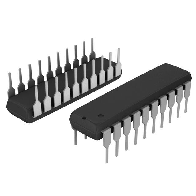
引脚分配: - 1: G(数据使能输入,低电平有效) - 2, 5, 6, 9, 12, 15, 16, 19: 1Q至8Q(触发器输出) - 3, 4, 7, 8, 13, 14, 17, 18: 1D至8D(数据输入) - 11: CLOCK(时钟输入,低到高边沿触发) - 10: GND(地) - 20: Vcc(正电源电压)

参数特性: - 最大工作频率:66MHz(典型值,6V电源电压下) - 最大功耗:4μA(25°C环境温度下) - 噪声免疫力:Vcc的28%(最小值) - 输出阻抗:|IOL|=|IOLH|=4mA(最小值) - 工作电压范围:2V至6V - 与74系列377引脚和功能兼容

功能详解: M74HC377在时钟输入为高或低电平时,D输入对输出无影响。所有输入都配备了防静电和瞬态过电压保护电路。在使能输入G为低时,满足设置时间要求的D输入信息会在时钟脉冲的上升沿被传输到Q输出。时钟触发发生在特定的电压水平,并且与传播延迟无关。

应用信息: M74HC377适用于需要高速和低功耗的数字电路,如数据存储、计数器、寄存器等。
M74HC377B1R 价格&库存

很抱歉,暂时无法提供与“M74HC377B1R”相匹配的价格&库存,您可以联系我们找货

免费人工找货