M95320-W M95320-R
M95320-DF
32-Kbit serial SPI bus EEPROM with high-speed clock
Datasheet - production data
Features
• Compatible with the Serial Peripheral Interface
(SPI) bus
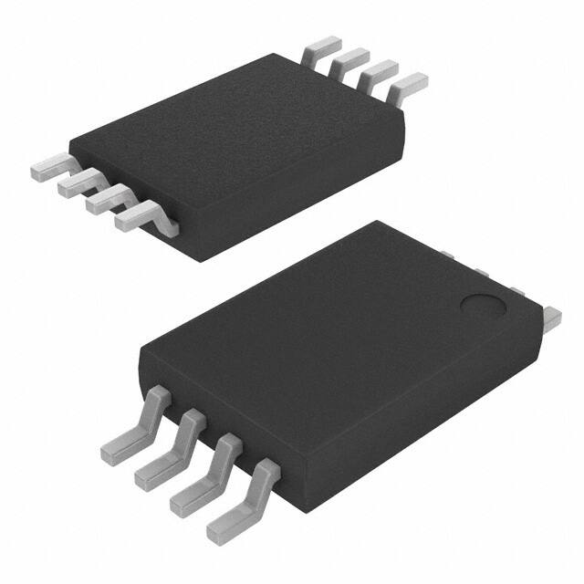
SO8 (MN)
150 mil width
• Memory array
– 32 Kb (4 Kbytes) of EEPROM
– Page size: 32 bytes
• Write
– Byte Write within 5 ms
– Page Write within 5 ms
• Additional Write lockable page (Identification
page)
TSSOP8 (DW)
169 mil width
• Write Protect: quarter, half or whole memory
array
• High-speed clock: 20 MHz
UFDFPN8
2 × 3 mm
• Single supply voltage:
– 2.5 V to 5.5 V for M95320-W
– 1.8 V to 5.5 V for M95320-R
– 1.7 V to 5.5 V for M95320-DF
• Operating temperature range: from -40°C up to
+85°C
• Enhanced ESD protection
• More than 4 million Write cycles
• More than 200-year data retention
• Packages:
– SO8 (ECOPACK2®)
– TSSOP8 (ECOPACK2®)
– UFDFPN8 (ECOPACK2®)
November 2015
This is information on a product in full production.
DocID5711 Rev 16
1/48
www.st.com
�Contents
M95320-W M95320-R M95320-DF
Contents
1
Description . . . . . . . . . . . . . . . . . . . . . . . . . . . . . . . . . . . . . . . . . . . . . . . . . 6
2
Memory organization . . . . . . . . . . . . . . . . . . . . . . . . . . . . . . . . . . . . . . . . 8
3
Signal description . . . . . . . . . . . . . . . . . . . . . . . . . . . . . . . . . . . . . . . . . . . 9
4
3.1
Serial Data Output (Q) . . . . . . . . . . . . . . . . . . . . . . . . . . . . . . . . . . . . . . . . 9
3.2
Serial Data Input (D) . . . . . . . . . . . . . . . . . . . . . . . . . . . . . . . . . . . . . . . . . . 9
3.3
Serial Clock (C) . . . . . . . . . . . . . . . . . . . . . . . . . . . . . . . . . . . . . . . . . . . . . 9
3.4
Chip Select (S) . . . . . . . . . . . . . . . . . . . . . . . . . . . . . . . . . . . . . . . . . . . . . . 9
3.5
Hold (HOLD) . . . . . . . . . . . . . . . . . . . . . . . . . . . . . . . . . . . . . . . . . . . . . . . . 9
3.6
Write Protect (W) . . . . . . . . . . . . . . . . . . . . . . . . . . . . . . . . . . . . . . . . . . . 10
3.7
VCC supply voltage . . . . . . . . . . . . . . . . . . . . . . . . . . . . . . . . . . . . . . . . . . 10
3.8
VSS ground . . . . . . . . . . . . . . . . . . . . . . . . . . . . . . . . . . . . . . . . . . . . . . . . 10
Connecting to the SPI bus . . . . . . . . . . . . . . . . . . . . . . . . . . . . . . . . . . . 11
4.1
5
Operating features . . . . . . . . . . . . . . . . . . . . . . . . . . . . . . . . . . . . . . . . . 13
5.1
6
SPI modes . . . . . . . . . . . . . . . . . . . . . . . . . . . . . . . . . . . . . . . . . . . . . . . . 12
Supply voltage (VCC) . . . . . . . . . . . . . . . . . . . . . . . . . . . . . . . . . . . . . . . . 13
5.1.1
Operating supply voltage (VCC) . . . . . . . . . . . . . . . . . . . . . . . . . . . . . . . 13
5.1.2
Device reset . . . . . . . . . . . . . . . . . . . . . . . . . . . . . . . . . . . . . . . . . . . . . . 13
5.1.3
Power-up conditions . . . . . . . . . . . . . . . . . . . . . . . . . . . . . . . . . . . . . . . 13
5.1.4
Power-down . . . . . . . . . . . . . . . . . . . . . . . . . . . . . . . . . . . . . . . . . . . . . . 14
5.2
Active Power and Standby Power modes . . . . . . . . . . . . . . . . . . . . . . . . 14
5.3
Hold condition . . . . . . . . . . . . . . . . . . . . . . . . . . . . . . . . . . . . . . . . . . . . . . 14
5.4
Status Register . . . . . . . . . . . . . . . . . . . . . . . . . . . . . . . . . . . . . . . . . . . . . 15
5.5
Data protection and protocol control . . . . . . . . . . . . . . . . . . . . . . . . . . . . 15
Instructions . . . . . . . . . . . . . . . . . . . . . . . . . . . . . . . . . . . . . . . . . . . . . . . 16
6.1
Write Enable (WREN) . . . . . . . . . . . . . . . . . . . . . . . . . . . . . . . . . . . . . . . 17
6.2
Write Disable (WRDI) . . . . . . . . . . . . . . . . . . . . . . . . . . . . . . . . . . . . . . . . 18
6.3
Read Status Register (RDSR) . . . . . . . . . . . . . . . . . . . . . . . . . . . . . . . . . 19
6.3.1
2/48
WIP bit . . . . . . . . . . . . . . . . . . . . . . . . . . . . . . . . . . . . . . . . . . . . . . . . . . 19
DocID5711 Rev 16
�M95320-W M95320-R M95320-DF
6.3.2
WEL bit . . . . . . . . . . . . . . . . . . . . . . . . . . . . . . . . . . . . . . . . . . . . . . . . . 19
6.3.3
BP1, BP0 bits . . . . . . . . . . . . . . . . . . . . . . . . . . . . . . . . . . . . . . . . . . . . . 19
6.3.4
SRWD bit . . . . . . . . . . . . . . . . . . . . . . . . . . . . . . . . . . . . . . . . . . . . . . . . 20
6.4
Write Status Register (WRSR) . . . . . . . . . . . . . . . . . . . . . . . . . . . . . . . . . 21
6.5
Read from Memory Array (READ) . . . . . . . . . . . . . . . . . . . . . . . . . . . . . . 23
6.6
Write to Memory Array (WRITE) . . . . . . . . . . . . . . . . . . . . . . . . . . . . . . . 24
6.6.1
7
Contents
Cycling with Error Correction Code (ECC) . . . . . . . . . . . . . . . . . . . . . . 26
6.7
Read Identification Page (available only in M95320-D devices) . . . . . . . 27
6.8
Write Identification Page (available only in M95320-D devices) . . . . . . . 28
6.9
Read Lock Status (available only in M95320-D devices) . . . . . . . . . . . . . 29
6.10
Lock ID (available only in M95320-D devices) . . . . . . . . . . . . . . . . . . . . . 30
Power-up and delivery state . . . . . . . . . . . . . . . . . . . . . . . . . . . . . . . . . . 31
7.1
Power-up state . . . . . . . . . . . . . . . . . . . . . . . . . . . . . . . . . . . . . . . . . . . . . 31
7.2
Initial delivery state . . . . . . . . . . . . . . . . . . . . . . . . . . . . . . . . . . . . . . . . . . 31
8
Maximum ratings . . . . . . . . . . . . . . . . . . . . . . . . . . . . . . . . . . . . . . . . . . . 32
9
DC and AC parameters . . . . . . . . . . . . . . . . . . . . . . . . . . . . . . . . . . . . . . 33
10
Package information . . . . . . . . . . . . . . . . . . . . . . . . . . . . . . . . . . . . . . . . 41
10.1
SO8N package information . . . . . . . . . . . . . . . . . . . . . . . . . . . . . . . . . . . 41
10.2
TSSOP8 package information . . . . . . . . . . . . . . . . . . . . . . . . . . . . . . . . . 43
10.3
UFDFN8 package information . . . . . . . . . . . . . . . . . . . . . . . . . . . . . . . . . 44
11
Part numbering . . . . . . . . . . . . . . . . . . . . . . . . . . . . . . . . . . . . . . . . . . . . 45
12
Revision history . . . . . . . . . . . . . . . . . . . . . . . . . . . . . . . . . . . . . . . . . . . 47
DocID5711 Rev 16
3/48
3
�List of tables
M95320-W M95320-R M95320-DF
List of tables
Table 1.
Table 2.
Table 3.
Table 4.
Table 5.
Table 6.
Table 7.
Table 8.
Table 9.
Table 10.
Table 11.
Table 12.
Table 13.
Table 14.
Table 15.
Table 16.
Table 17.
Table 18.
Table 19.
Table 20.
Table 21.
Table 22.
Table 23.
Table 24.
4/48
Signal names . . . . . . . . . . . . . . . . . . . . . . . . . . . . . . . . . . . . . . . . . . . . . . . . . . . . . . . . . . . . 6
Write-protected block size . . . . . . . . . . . . . . . . . . . . . . . . . . . . . . . . . . . . . . . . . . . . . . . . . 15
Instruction set . . . . . . . . . . . . . . . . . . . . . . . . . . . . . . . . . . . . . . . . . . . . . . . . . . . . . . . . . . . 16
Significant bits within the two address bytes . . . . . . . . . . . . . . . . . . . . . . . . . . . . . . . . . . . 16
Status Register format . . . . . . . . . . . . . . . . . . . . . . . . . . . . . . . . . . . . . . . . . . . . . . . . . . . . 20
Protection modes . . . . . . . . . . . . . . . . . . . . . . . . . . . . . . . . . . . . . . . . . . . . . . . . . . . . . . . . 22
Absolute maximum ratings . . . . . . . . . . . . . . . . . . . . . . . . . . . . . . . . . . . . . . . . . . . . . . . . . 32
Operating conditions (M95320-W, device grade 6) . . . . . . . . . . . . . . . . . . . . . . . . . . . . . . 33
Operating conditions (M95320-R, device grade 6) . . . . . . . . . . . . . . . . . . . . . . . . . . . . . . . 33
Operating conditions (M95320-DF, device grade 6) . . . . . . . . . . . . . . . . . . . . . . . . . . . . . . 33
AC measurement conditions. . . . . . . . . . . . . . . . . . . . . . . . . . . . . . . . . . . . . . . . . . . . . . . . 33
Cycling performance by groups of four bytes . . . . . . . . . . . . . . . . . . . . . . . . . . . . . . . . . . . 34
Memory cell data retention . . . . . . . . . . . . . . . . . . . . . . . . . . . . . . . . . . . . . . . . . . . . . . . . . 34
Capacitance . . . . . . . . . . . . . . . . . . . . . . . . . . . . . . . . . . . . . . . . . . . . . . . . . . . . . . . . . . . . 34
DC characteristics (M95320-W, device grade 6) . . . . . . . . . . . . . . . . . . . . . . . . . . . . . . . . 35
DC characteristics (M95320-R, device grade 6) . . . . . . . . . . . . . . . . . . . . . . . . . . . . . . . . . 36
DC characteristics (M95320-DF, device grade 6). . . . . . . . . . . . . . . . . . . . . . . . . . . . . . . . 37
AC characteristics (M95320-W, device grade 6) . . . . . . . . . . . . . . . . . . . . . . . . . . . . . . . . 38
AC characteristics (M95320-R, M95320-DF, device grade 6) . . . . . . . . . . . . . . . . . . . . . . 39
SO8N – 8-lead plastic small outline, 150 mils body width,
package mechanical data . . . . . . . . . . . . . . . . . . . . . . . . . . . . . . . . . . . . . . . . . . . . . . . . . . 41
TSSOP8 – 8-lead thin shrink small outline, 3 x 4.4 mm, 0.5 mm pitch,
package mechanical data . . . . . . . . . . . . . . . . . . . . . . . . . . . . . . . . . . . . . . . . . . . . . . . . . . 43
UFDFPN8 (MLP8) – 8-lead ultra thin fine pitch dual flat package no lead
2 x 3 mm, data . . . . . . . . . . . . . . . . . . . . . . . . . . . . . . . . . . . . . . . . . . . . . . . . . . . . . . . . . . 44
Ordering information scheme . . . . . . . . . . . . . . . . . . . . . . . . . . . . . . . . . . . . . . . . . . . . . . . 45
Document revision history . . . . . . . . . . . . . . . . . . . . . . . . . . . . . . . . . . . . . . . . . . . . . . . . . 47
DocID5711 Rev 16
�M95320-W M95320-R M95320-DF
List of figures
List of figures
Figure 1.
Figure 2.
Figure 3.
Figure 4.
Figure 5.
Figure 6.
Figure 7.
Figure 8.
Figure 9.
Figure 10.
Figure 11.
Figure 12.
Figure 13.
Figure 14.
Figure 15.
Figure 16.
Figure 17.
Figure 18.
Figure 19.
Figure 20.
Figure 21.
Figure 22.
Figure 23.
Figure 24.
Figure 25.
Logic diagram . . . . . . . . . . . . . . . . . . . . . . . . . . . . . . . . . . . . . . . . . . . . . . . . . . . . . . . . . . . . 6
8-pin package connections (top view) . . . . . . . . . . . . . . . . . . . . . . . . . . . . . . . . . . . . . . . . . 7
Block diagram . . . . . . . . . . . . . . . . . . . . . . . . . . . . . . . . . . . . . . . . . . . . . . . . . . . . . . . . . . . . 8
Bus master and memory devices on the SPI bus . . . . . . . . . . . . . . . . . . . . . . . . . . . . . . . . 11
SPI modes supported . . . . . . . . . . . . . . . . . . . . . . . . . . . . . . . . . . . . . . . . . . . . . . . . . . . . . 12
Hold condition activation . . . . . . . . . . . . . . . . . . . . . . . . . . . . . . . . . . . . . . . . . . . . . . . . . . . 14
Write Enable (WREN) sequence . . . . . . . . . . . . . . . . . . . . . . . . . . . . . . . . . . . . . . . . . . . . 17
Write Disable (WRDI) sequence . . . . . . . . . . . . . . . . . . . . . . . . . . . . . . . . . . . . . . . . . . . . . 18
Read Status Register (RDSR) sequence . . . . . . . . . . . . . . . . . . . . . . . . . . . . . . . . . . . . . . 19
Write Status Register (WRSR) sequence . . . . . . . . . . . . . . . . . . . . . . . . . . . . . . . . . . . . . . 21
Read from Memory Array (READ) sequence . . . . . . . . . . . . . . . . . . . . . . . . . . . . . . . . . . . 23
Byte Write (WRITE) sequence . . . . . . . . . . . . . . . . . . . . . . . . . . . . . . . . . . . . . . . . . . . . . . 24
Page Write (WRITE) sequence . . . . . . . . . . . . . . . . . . . . . . . . . . . . . . . . . . . . . . . . . . . . . 25
Read Identification Page sequence . . . . . . . . . . . . . . . . . . . . . . . . . . . . . . . . . . . . . . . . . . 27
Write identification page sequence . . . . . . . . . . . . . . . . . . . . . . . . . . . . . . . . . . . . . . . . . . 28
Read Lock Status sequence . . . . . . . . . . . . . . . . . . . . . . . . . . . . . . . . . . . . . . . . . . . . . . . . 29
Lock ID sequence . . . . . . . . . . . . . . . . . . . . . . . . . . . . . . . . . . . . . . . . . . . . . . . . . . . . . . . . 30
AC measurement I/O waveform . . . . . . . . . . . . . . . . . . . . . . . . . . . . . . . . . . . . . . . . . . . . . 33
Serial input timing . . . . . . . . . . . . . . . . . . . . . . . . . . . . . . . . . . . . . . . . . . . . . . . . . . . . . . . . 40
Hold timing . . . . . . . . . . . . . . . . . . . . . . . . . . . . . . . . . . . . . . . . . . . . . . . . . . . . . . . . . . . . . 40
Serial output timing . . . . . . . . . . . . . . . . . . . . . . . . . . . . . . . . . . . . . . . . . . . . . . . . . . . . . . . 40
SO8N – 8-lead plastic small outline, 150 mils body width, package outline . . . . . . . . . . . . 41
SO8N – 8-lead plastic small outline, 150 mils body width,
package recommended footprint . . . . . . . . . . . . . . . . . . . . . . . . . . . . . . . . . . . . . . . . . . . . 42
TSSOP8 – 8-lead thin shrink small outline, 3 x 4.4 mm, 0.5 mm pitch,
package outline. . . . . . . . . . . . . . . . . . . . . . . . . . . . . . . . . . . . . . . . . . . . . . . . . . . . . . . . . . 43
UFDFPN8 (MLP8) – 8-lead ultra thin fine pitch dual flat no lead, package outline. . . . . . . 44
DocID5711 Rev 16
5/48
5
�Description
1
M95320-W M95320-R M95320-DF
Description
The M95320 devices are Electrically Erasable PROgrammable Memories (EEPROMs)
organized as 4096 x 8 bits, accessed through the SPI bus.
The M95320 devices can operate with a supply range from 1.7 V to 5.5 V, and are
guaranteed over the -40 °C/+85 °C temperature range.
The M95320-D offers an additional page, named the Identification Page (32 bytes). The
Identification Page can be used to store sensitive application parameters which can be
(later) permanently locked in Read-only mode.
Figure 1. Logic diagram
6##
$
1
#
3
-��XXX
7
(/,$
633
!)�����#
The SPI bus signals are C, D and Q, as shown in Figure 1 and Table 1. The device is
selected when Chip Select (S) is driven low. Communications with the device can be
interrupted when the HOLD is driven low.
Table 1. Signal names
Signal name
6/48
Function
Direction
C
Serial Clock
Input
D
Serial Data Input
Input
Q
Serial Data Output
Output
S
Chip Select
Input
W
Write Protect
Input
HOLD
Hold
Input
VCC
Supply voltage
-
VSS
Ground
-
DocID5711 Rev 16
�M95320-W M95320-R M95320-DF
Description
Figure 2. 8-pin package connections (top view)
-��XXX
3 �
1 �
7 �
633 �
�
�
�
�
6##
(/,$
#
$
!)�����$
1. See Section 10: Package information for package dimensions, and how to identify pin-1.
DocID5711 Rev 16
7/48
40
�Memory organization
2
M95320-W M95320-R M95320-DF
Memory organization
The memory is organized as shown in the following figure.
Figure 3. Block diagram
+2/'
:
6
+LJK�YROWDJH�
JHQHUDWRU
&RQWURO�ORJLF
&
'
4
,�2�VKLIW�UHJLVWHU
$GGUHVV�UHJLVWHU
DQG�FRXQWHU
'DWD�UHJLVWHU
6WDWXV�
UHJLVWHU
很抱歉,暂时无法提供与“M95320-DRDW6TP”相匹配的价格&库存,您可以联系我们找货
免费人工找货- 国内价格
- 1+6.70680
- 200+5.58900
- 500+4.47120
- 1000+3.72600