MC3303
MC3403 - MC3503
LOW POWER
QUAD BIPOLAR OPERATIONAL AMPLIFIERS
■ SHORT-CIRCUIT PROTECTED OUTPUTS
■ CLASS AB OUTPUT STAGE FOR MINIMAL
CROSSOVER DISTORTION
■ SINGLE SUPPLY OPERATION: +3V TO +36V
■ DUAL SUPPLIES: ±15V TO ±18V
■ LOW INPUT BIAS CURRENT: 500nA MAX
■ INTERNALLY COMPENSATED
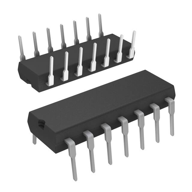
N
DIP14
(Plastic Package)
D
SO14
(Plastic Micropackage)
■ SIMILAR PERFORMANCE TO POPULAR
UA741
DESCRIPTION
The MC3403 is a low-cost, quad operational amplifier with true differential inputs. The device has
electrical characteristics similar to the popular
UA741. However the MC3403, has several distinct advantages over standard operational amplifiers types in single supply applications. The quad
amplifier can operate at supply voltage as low as 3
Volts or as high as 36 volts with quiescent currents
about one third of those associated with the
UA741 (on a per amplifier basis). The common-mode input range includes the negative supply, thereby eliminating the necessity for external
biasing components in many applications.
Temperature
Range
MC3303
-40°C, +105°C
MC3403
0°C, +70°C
MC3503
-55°C, +125°C
Example : MC3403N
PIN CONNECTIONS (top view)
Output 1 1
ORDER CODE
Part
Number
P
TSSOP14
(Thin Shrink Small Outline Package)
Package
Inverting Input 1 2
Non-inverting Input 1 3
14 Output 4
-
-
13 Inverting Input 4
+
+
12 Non-inverting Input 4
11 VCC -
N
D
P
VCC + 4
•
•
•
•
•
•
•
•
•
Non-inverting Input 2 5
+
+
10 Non-inverting Input 3
Inverting Input 2 6
-
-
9
Inverting Input 3
8
Output 3
Output 2 7
N = Dual in Line Package (DIP)
D = Small Outline Package (SO) - also available in Tape & Reel (DT)
P = Thin Shrink Small Outline Package (TSSOP) - only available
in Tape & Reel (PT)
November 2001
1/10
�MC3303 - MC3403 - MC3503
SCHEMATIC DIAGRAM (each amplifier)
Output
V
Q19
(1 stage)
CC
Q18
Q20
Q17
Q27
Q16
Q23
C1
8pF
R4
31k Ω
Q29
Q28
Q1
Q15
Non-inverting
input
R6
0.7k Ω
Q22
Q13
R3
25 Ω
Q24
Q9
R2
37 kΩ
Q12
Inverting
input
Q21
Q2
Q6
Q5
Q4
Q3
Q30
Q11
Q25
Q7
R5
8.2k Ω
Q10
Q14
Q8
R1
12k Ω
V
CC
(Ground)
SCHEMATIC DIAGRAM
DUAL SUPPLIES
+3V to +30V
V CC
V CC
1.5V to 18V
1.5V to 18V
V CC
V CC
ABSOLUTE MAXIMUM RATINGS
Symbol
VCC
Parameter
Supply voltage
1)
Vi
Input Voltage
Vid
Differential Input Voltage
Output Short-circuit Duration
2)
Ptot
Power Dissipation
Toper
Operating Free-air Temperature Range
Tstg
Storage Temperature Range
1.
2.
2/10
MC3503
MC3403
MC3303
Unit
±18 or 36
V
±18
V
±36
V
Infinite
500
-55 to +125
0 to +70
-65 to +150
mW
-40 to +105
°C
°C
For supply voltage less than ±15V, the absolute maximum input voltage is equal to the supply voltage.
Any of the amplifier outputs can be shorted to ground indefinitly; however more than one should not be simultaneously shorted as the maximum
junction will be exceeded.
�MC3303 - MC3403 - MC3503
ELECTRICAL CHARACTERISTICS
VCC = ±15V, Tamb = 25°C (unless otherwise specified)
Symbol
Parameter
Min.
Typ.
Max.
Unit
Vio
Input Offset Voltage (Rs ≤ 10kΩ)
Tamb = 25°C
Tmin ≤ Tamb ≤ Tmax
1
5
6
mV
Iio
Input Offset Current
Tamb = 25°C
Tmin ≤ Tamb ≤ Tmax
5
50
200
nA
Iib
Input Bias Current
Tamb = 25°C
Tmin ≤ Tamb ≤ Tmax
40
500
800
nA
Avd
Large Signal Voltage Gain (Vo = ±10V, RL = 2kΩ)
Tamb = 25°C
Tmin ≤ Tamb ≤ Tmax
50
25
200
V/mV
SVR
Supply Voltage Rejection Ratio (Rs ≤ 10kΩ)
Tamb = 25°C
Tmin ≤ Tamb ≤ Tmax
77
77
90
dB
Supply Current, all Amp, no load
Tamb = 25°C
Icc
Tmin ≤ Tamb ≤ Tmax
2.8
MC3503
MC3503
Vicm
Input Common Mode Voltage Range
Tamb = 25°C
Tmin ≤ Tamb ≤ Tmax
-15
-15
CMR
Common Mode Rejection Ratio (Rs ≤ 10kΩ)
Tamb = 25°C
Tmin ≤ Tamb ≤ Tmax
70
70
90
Output Short-circuit Current
10
30
12
10
12
10
13.5
13
0.35
0.5
Ios
Output Voltage Swing
Tamb = 25°C
±Vopp
Tmin ≤ Tamb ≤ Tmax
RL ≤ 10kΩ
RL ≤ 2kΩ
RL ≤ 10kΩ
RL ≤ 2kΩ
+13
+13
SR
Slew Rate (VI = ±10V, RL = 2kΩ, CL = 100pF, Tamb = 25°C,
unity gain)
tr, tf
Rsie Time (Vo = ±20mV, RL = 2kΩ, CL = 100pF,Tamb = 25°C,
unity gain)
0.18
KOV
Overshoot (VI = ±20mV, RL = 2kΩ, CL = 100pF, Tamb = 25°C,
unity gain)
10
mA
V
dB
45
mA
V
V/µs
µs
%
1
ΜΩ
Output Impedance
75
Ω
Power Bandwidth (RL = 2kΩ, CL = 100pF, AV = 1, Tamb = 25°C,
VO = 2Vpp, THD ≤ 5%)
9
ZI
Input Impedance
ZO
Bom
B
7
4
8
5
Unity Gain Bandwidth Vo = 10mV, RL = 2kΩ, CL = 100pF, Tamb =
25°C, unity gain)
0.3
1
kHz
MHz
3/10
�MC3303 - MC3403 - MC3503
Symbol
Parameter
GBP
Gain Bandwith Product (VO = 10 mV, RL = 2kΩ, CL = 100pF
f =100kHz, Tamb = 25°C)
THD
Total Harmonic Distortion (f = 1kHz, Av = 20dB, RL = 2kΩ
CL = 100pF, Vo = 2Vpp, Tamb = 25°C)
Min.
Typ.
0.7
1
Max.
Unit
MHz
%
0.02
en
Equivalent Input Noise Voltage (f = 1kHz, Rs = 100Ω
43
nV
-----------Hz
φm
Phase Margin
60
Degrees
DVio
Input Offset Voltage Drift
Tmin ≤ Tamb ≤ Tmax
10
DIio
Input Offset Current Drift
Tmin ≤ Tamb ≤ Tmax
50
Vo1/Vo2 Channel Separation
µV/°C
pA/°C
120
dB
ELECTRICAL CHARACTERISTICS
VCC+ = 5V, VCC- = Ground, Tamb = 25°C (unless otherwise specified)
Symbol
Parameter
Min.
Typ.
Max.
Unit
Vio
Input Offset Voltage (Rs ≤ 10kΩ)
Tamb = 25°C
Tmin ≤ Tamb ≤ Tmax
1
5
6
mV
Iio
Input Offset Current
Tamb = 25°C
Tmin ≤ Tamb ≤ Tmax
5
50
200
nA
Iib
Input Bias Current
Tamb = 25°C
Tmin ≤ Tamb ≤ Tmax
40
500
800
nA
Avd
Large Signal Voltage Gain (Vo = 1.4Vto 2.4V, RL = 2kΩ)
Tamb = 25°C
Tmin ≤ Tamb ≤ Tmax
10
5
200
V/mV
SVR
Supply Voltage Rejection Ratio (Rs ≤ 10kΩ)
Tamb = 25°C
Tmin ≤ Tamb ≤ Tmax
77
77
90
dB
Icc
Vopp
4/10
Supply Current, all Amp, no load
MC3503
Output Voltage Range (RL = 10kΩ)
VCC = +5V
+5 < VCC ≤ +30V
2.8
3.3
3.5
+
+
VCC -2V VCC -1.7V
7
4
mA
V
�MC3303 - MC3403 - MC3503
CIRCUIT DESCRIPTION
The MC3403 is made using four internally compensated, two-stage operational amplifiers. The
first stage of each consists of differential input devices Q24 and Q22 with input buffer transistors
Q25 and Q21 and the differential to single ended
converter Q3 and Q4. The first stage performs not
only the first stage gain function but also performs
the level shifting and transonductance reduction
functions. By reducing the transconductance a
smaller compensation capacitor (only 8pF) can be
employed, thus saving chip area.
The transconductance reduction is accomplished
by splitting the collectors of Q24 and Q22. Another
feature of this input stage is that the input common-mode range can include the negative supply
fo ground, in single supply operation, without saturation either the input devices or the differential
to single-ended converter.
The second stage consists of a standard current
source load amplifier stage. The output stage is
unique because it allows the output to swing to
ground in single supply operation and yet does not
exhibit any crossover distortion in split supply operations. This is possible because class AB operation is utilized.
Each amplifier is biased from an internal voltage
regulator which has a low temperature coefficient
thus giving each amplifier good temperature characteristics as well as excellent power supply rejection.
TYPICAL PERFORMANCE CURVES
AV = 100
APPLICATION INFORMATION
VOLTAGE REFERENCE
V CC
R2
10kΩ
V CC
1/4
MC3403
VO
R1
10kΩ
VO =
R1
V CC
R1 + R2
VO = 1 V CC
2
WIEN BRIDGE OSCILLATOR
50kΩ
5kΩ
V CC
10kΩ
V(ref)
1/4
MC3403
VO
V(ref) = 1 V CC
2
R
R
C
C
fO =
1
2 π RC
For
f O = 1kHz
R = 16kΩ
C = 0.01µF
20µs/div.
5/10
�MC3303 - MC3403 - MC3503
HIGH IMPEDANCE DIFFERENTIAL AMPLIFIER
e1
1 R
C
1/4
MC3403
COMPARATOR WITH HYSTERESIS
R
R2
Hysteresis
V OH
VO
R1
V (ref)
a R1
R1
1/4
MC3403
1/4
MC3403
eo
VO
VI
b R1
V OL
R1
[V OL- V(ref) ] + V(ref)
R1+R2
VIH = R1
[V OL- V(ref) ] + V(ref)
R1+R2
R1
H=
[V - V OL ]
R1+R2 OH
VIL =
1 R
C
1/4
MC3403
e2
e o = C (1 + a + b) ( e 2 - e 1 )
R
BI-QUAD FILTER
R
R
C
C
C1
e
R2
100kΩ
I
R
1/4
MC3403
100kΩ
1/4
MC3403
1/4
MC3403
V(ref)
V(ref)
Bandpass output
V(ref)
R3
R1
R2
C1
1/4
MC3403
R = 160k Ω
C = 0.001 µ F
R1 = 1.6M Ω
R2 = 1.6M Ω
R3 = 1.6M Ω
Notch output
Where T BP = Center frequency gain
V(ref)
T N = Passband notch gain
FUNCTION GENERATOR
V (ref)
R2
300kΩ
Triangle wave output
1 V
=
2 CC
V (ref)
1/4
MC3403
R3
75kΩ
1/4
MC3403
R1
100kΩ
C
V (ref)
R
R1 + R2
f=
4 CR f R1
6/10
f
if R3 =
R2 R1
R2 + R1
Square wave output
VI H
VI L
V (ref)
�MC3303 - MC3403 - MC3503
MULTIPLE FEEDBACK BANDPASS FILTER
R3
C
R1
VCC
C
eI
1/4
MC3403
eo
CO
C O = 10C
R2
V (ref)
V (ref) = 1 VCC
2
Q
p foC
R1 = R3
2A (fo)
R5
R2 = R1
4Q2 R1-R5
R3 =
Given fo = center frequency ; chosse values fo, C than
A (fo) = gain at center frequency
For less than 10% error from operational amplifier
QoFo < 0.1 where fo and BW are expressed in Hz
BW
If source impedance varies, filter may be preceded with voltage
follower buffer to stabilize filter parameters
TYPICAL PERFORMANCE CURVES
7/10
�MC3303 - MC3403 - MC3503
PACKAGE MECHANICAL DATA
14 PINS - PLASTIC PACKAGE
Millimeters
Inches
Dimensions
Min.
a1
B
b
b1
D
E
e
e3
F
i
L
Z
8/10
Typ.
0.51
1.39
Max.
Min.
1.65
0.020
0.055
0.5
0.25
Typ.
0.065
0.020
0.010
20
0.787
8.5
2.54
15.24
0.335
0.100
0.600
7.1
5.1
0.280
0.201
3.3
1.27
Max.
0.130
2.54
0.050
0.100
�MC3303 - MC3403 - MC3503
PACKAGE MECHANICAL DATA
14 PINS - PLASTIC MICROPACKAGE (SO)
G
c1
b1
e
a1
b
A
a2
C
L
s
e3
E
D
M
8
1
7
F
14
Millimeters
Inches
Dimensions
Min.
A
a1
a2
b
b1
C
c1
D (1)
E
e
e3
F (1)
G
L
M
S
Typ.
Max.
Min.
1.75
0.2
1.6
0.46
0.25
0.1
0.35
0.19
Typ.
0.069
0.008
0.063
0.018
0.010
0.004
0.014
0.007
0.5
Max.
0.020
45° (typ.)
8.55
5.8
8.75
6.2
0.336
0.228
1.27
7.62
3.8
4.6
0.5
0.344
0.244
0.050
0.300
4.0
5.3
1.27
0.68
0.150
0.181
0.020
0.157
0.208
0.050
0.027
8° (max.)
Note : (1) D and F do not include mold flash or protrusions - Mold flash or protrusions shall not exceed 0.15mm (.066 inc) ONLY FOR DATA BOOK.
9/10
�MC3303 - MC3403 - MC3503
PACKAGE MECHANICAL DATA
14 PINS - THIN SHRINK SMALL OUTLINE PACKAGE
k
c
C
SEATING
PLANE
E1
L1
L
0,25 mm
.010 inch
GAGE PLANE
E
A
A2
7
aaa
C
D
8
e
b
A1
14
1
PIN 1 IDENTIFICATION
Millimeters
Inches
Dimensions
Min.
A
A1
A2
b
c
D
E
E1
e
k
L
L1
aaa
0.05
0.80
0.19
0.09
4.90
4.30
0°
0.450
Typ.
1.00
5.00
6.40
4.40
0.65
0.600
1.00
Max.
Min.
1.20
0.15
1.05
0.30
0.20
5.10
0.01
0.031
0.007
0.003
0.192
4.50
0.169
8°
0.750
0°
0.018
0.100
Typ.
0.039
0.196
0.252
0.173
0.025
0.024
0.039
Max.
0.05
0.006
0.041
0.15
0.012
0.20
0.177
8°
0.030
0.004
Information furnished is believed to be accurate and reliable. However, STMicroelectronics assumes no responsibility for the
consequences of use of such information nor for any infringement of patents or other rights of third parties which may result from
its use. No license is granted by implication or otherwise under any patent or patent rights of STMicroelectronics. Specifications
mentioned in this publication are subject to change without notice. This publication supersedes and replaces all information
previously supplied. STMicroelectronics products are not authorized for use as critical components in life support devices or
systems without express written approval of STMicroelectronics.
© The ST logo is a registered trademark of STMicroelectronics
© 2001 STMicroelectronics - Printed in Italy - All Rights Reserved
STMicroelectronics GROUP OF COMPANIES
Australia - Brazil - Canada - China - Finland - France - Germany - Hong Kong - India - Israel - Italy - Japan - Malaysia
Malta - Morocco - Singapore - Spain - Sweden - Switzerland - United Kingdom - United States
© http://www.st.com
10/10
�