MSS40, MSS50
Back to back SCR module
Table 1.
Main features
Symbol
Value
Unit
IT(RMS)
55 and 70
A
VDRM/VRRM
800 and 1200
V
IGT
50
mA
G2
A2
A1
G1
Description
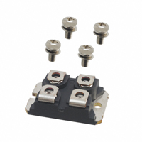
ISOTOP
Packaged in ISOTOP modules, the MSS40 /
MSS50 Series is based on two back-to-back SCR
configurations, providing high noise immunity.
They are suitable for high power applications such
as solid state relays, heating control systems,
welding equipment, motor control circuits...
Table 2.
e
t
le
The compactness of the ISOTOP package allows
high power density and optimized power bus
connections. Thanks to their internal ceramic pad,
they provide high voltage insulation (2500 VRMS),
complying with UL standards (File ref: E81734).
Figure 1.
o
r
P
e
1: Thyristor 2 Anode (A2)
2: Thyristor 2 Gate (G2)
3: Thyristor 1 Anode (A1)
4: Thyristor 2 Gate (G1)
t
e
l
o
s
b
O
July 2007
)
s
(
ct
Pin connections
du
4
o
r
P
Order codes
Part numbers
MSS40-1200
MSS50-800
MSS50-800
MSS50-1200
MSS50-1200
G1
3
A1
1
Marking
MSS40-1200
so
b
O
-
c
u
d
)
s
t(
A2
2
G2
Rev 4
1/7
www.st.com
7
�Characteristics
MSS40, MSS50
1
Characteristics
Table 3.
Absolute ratings (limiting values)
Value
Symbol
Parameter
Unit
VDRM/VRRM Repetitive peak off-state voltage
IT(RMS)
ITSM
2t
I
1200
800
1200
Tc = 80° C
RMS on-state current
55
Tc = 85° C
Non repetitive surge peak on-state
current
tp = 16.7 ms
I2t
tp = 10 ms
Tj = 25° C
Tj = 25° C
tp = 20 ms
Value for fusing
420
630
400
600
A
800
1800
A2S
F = 120 Hz
Tj = 125° C
50
IGM
Peak gate current
tp = 20 µs
Tj = 125° C
4
Tj = 125° C
1
Average gate power dissipation
Tstg
Tj
Storage junction temperature range
Operating junction temperature range
VRGM
Maximum peak reverse gate voltage
RL = 33 Ω
(s)
VGT
VGD
VD = VDRM
RL = 3.3 kΩ
IH
IT = 500 mA
Gate open
IL
IG = 1.2 IGT
IDRM
IRRM
Table 5.
- 40 to + 150
- 40 to + 125
od
5
W
°C
V
ct
b
O
-
Unit
MSS40
MSS50
MIN.
5
MAX.
50
MAX.
1.3
mA
V
V
mA
MAX.
120
mA
Tj = 125° C
MIN.
1000
V/µs
Tj = 25° C
MAX.
Threshold voltage
Tj = 125° C
MAX.
Dynamic resistance
Tj = 125° C
MAX.
u
d
o
r
P
e
Gate open
tp = 380 µs
ITM = 100 A
tp = 380 µs
VDRM = VRRM
Tj = 125° C
Value
80
Tj = 25° C
Tj = 125° C
MAX.
1.7
1.7
0.85
11
V
V
7
mΩ
20
µA
10
mA
Thermal reistances
Symbol
Rth(j-c)
uc
0.2
t
e
l
o
bs
Rd
A
MIN.
ITM = 80 A
Vt0
)
s
t(
MAX.
VD = 67 % VDRM
VTM
so
Test Conditions
VD = 12 V
dV/dt
Pr
A/µs
Electrical characteristics (Tj = 25° C, unless otherwise specified)
Symbol
IGT
e
t
le
V
A
70
Critical rate of rise of on-state current
IG = 2 x IGT , tr ≤ 100 ns
Table 4.
2/7
MSS50
dI/dt
PG(AV)
O
MSS40
Parameter
Value
MSS40
0.6
MSS50
0.45
Junction to case (AC)
Unit
° C/W
�MSS40, MSS50
Figure 2.
Characteristics
Maximum average power
Figure 3.
dissipation versus average on-state
current
P(W)
Average and DC on-state current
versus case temperature
IT(RMS)(A)
100
80
α = 180°
90
α = 180°
MSS50
70
80
60
70
MSS40
MSS50
MSS40
60
50
50
40
40
30
30
180°
20
10
20
α
α
10
IT(RMS)(A)
Tcase(°C)
0
0
0
10
Figure 4.
20
30
40
50
60
70
0
80
Relative variation of thermal
impedance versus pulse duration
25
Figure 5.
50
2.5
2.0
e
t
le
0.5
1.5
so
1.0
0.2
b
O
0.5
tp(s)
1E-2
Figure 6.
1E-1
s
b
O
600
MSS40
150
)
s
t(
c
u
d
o
r
P
IGT
Tj(°C)
0.0
1E+1
-40
t
c
u
d
o
r
P
e
-20
0
20
40
60
80
100
120
140
160
Non-repetitive surge peak on-state
current for a sinusoidal pulse with
width tp < 10 ms, and
corresponding values of I2t
2
2
ITSM(A), I t (A s)
5000
MSS50
500
125
IH & IL
Surge peak on-state current versus Figure 7.
number of cycles
t
e
l
o
ITSM(A)
700
(s)
1E+0
100
Relative variation of gate trigger
current and holding current versus
junction temperature
IGT,IH,IL[Tj] / IGT,IH,IL[Tj=25°C]
K=[Zth(j-c)/Rth(j-c)]
1.0
0.1
1E-3
75
Tj initial = 25°C
ITSM
t=20ms
One cycle
Non repetitive
Tj initial=25°C
400
1000
MSS50
Repetitive
TC=85°C
300
MSS50
I2t
MSS40
200
dI/dt limitation:
50A/µs
100
MSS40
Repetitive
TC=80°C
0
1
Number of cycles
10
100
tp(ms)
100
1000
0.01
0.10
1.00
10.00
3/7
�Ordering information scheme
Figure 8.
MSS40, MSS50
On-state characteristics (maximum Figure 9.
values) (MSS40)
ITM(A)
On-state characteristics (maximum
values) (MSS50)
ITM(A)
500
1000
Tj max.:
Vt0=0.85V
Rd=11mΩ
Tj max.:
Vt0=0.85V
Rd=7mΩ
100
Tj=max
100
Tj=max
Tj=25°C
Tj=25°C
VTM(V)
VTM(V)
10
10
0.0
2
0.5
1.0
1.5
2.0
2.5
3.0
3.5
4.0
4.5
5.0
5.5
6.0
0.0
1.0
2.0
4.0
Ordering information scheme
c
u
d
Figure 10. Ordering information scheme
SCR Module series
Current
40 = 55 A
50 = 70 A
)
s
(
ct
Voltage
800 = 800 V
1200 = 1200 V
u
d
o
r
P
e
t
e
l
o
s
b
O
4/7
3.0
o
s
b
O
-
e
t
le
o
r
P
MSS 40 - 800
5.0
)
s
t(
6.0
�MSS40, MSS50
3
Package information
Package information
●
Epoxy meets UL94, V0
●
Cooling method: by conduction (C)
●
Recommended torque value: 0.9 Nm (max. 1.2 Nm) for the 6 x M4 screws (2 x M4
screws recommended for mounting the package on the heatsink and the 4 provided
screws).
●
The screws supplied with the package are adapted for mounting on a board (or other
types of terminals) with a thickness of 0.6 mm min. and 2.2 mm max.
Table 6.
ISOTOP dimensions
Dimensions
Ref.
Millimeters
Inches
Min.
Max.
Min.
A
11.80
12.20
0.465
A1
8.90
9.10
B
7.8
8.20
C
0.75
C2
1.95
E
G2
A
C
0.030
0.033
2.05
0.077
0.081
37.80
38.20
1.488
1.504
so
31.50
31.70
1.240
1.248
E
25.15
25.50
0.990
1.004
E1
23.85
24.15
0.939
0.951
e
t
le
F
D
D1
)
s
(
ct
S
B
u
d
o
r
P
e
s
b
O
t
e
l
o
ØP
G1
E1
b
O
G
D1
0.358
0.85
C2
D
0.480
0.323
E2
P1
)
s
t(
0.307
A1
F1
od
uc
0.350
Max.
E2
Pr
24.80 typ.
0.976 typ.
G
14.90
15.10
0.587
0.594
G1
12.60
12.80
0.496
0.504
G2
3.50
4.30
0.138
0.169
F
4.10
4.30
0.161
0.169
F1
4.60
5.00
0.181
0.197
P
4.00
4.30
0.157
0.69
P1
4.00
4.40
0.157
0.173
S
30.10
30.30
1.185
1.193
In order to meet environmental requirements, ST offers these devices in ECOPACK®
packages. These packages have a lead-free second level interconnect. The category of
second level interconnect is marked on the package and on the inner box label, in
compliance with JEDEC Standard JESD97. The maximum ratings related to soldering
conditions are also marked on the inner box label. ECOPACK is an ST trademark.
ECOPACK specifications are available at: www.st.com.
5/7
�Ordering information
4
MSS40, MSS50
Ordering information
Table 7.
5
Ordering information
Part number
Marking
MSS40-1200
MSS40-1200
MSS50-800
MSS50-800
MSS50-1200
MSS50-1200
Package
Weight
Base qty
Delivery mode
ISOTOP
27 g
(without screws)
10
(with screws)
Tube
Revision history
Table 8.
Revision history
Changes
Revision
Sep-2000
3
Last release.
11-Jul-2007
4
Reformated to current standards. Removed MSS40-800 product.
c
u
d
e
t
le
)
s
(
ct
u
d
o
r
P
e
t
e
l
o
s
b
O
6/7
)
s
t(
Date
o
s
b
O
-
o
r
P
�MSS40, MSS50
Please Read Carefully:
Information in this document is provided solely in connection with ST products. STMicroelectronics NV and its subsidiaries (“ST”) reserve the
right to make changes, corrections, modifications or improvements, to this document, and the products and services described herein at any
time, without notice.
All ST products are sold pursuant to ST’s terms and conditions of sale.
)
s
t(
Purchasers are solely responsible for the choice, selection and use of the ST products and services described herein, and ST assumes no
liability whatsoever relating to the choice, selection or use of the ST products and services described herein.
c
u
d
No license, express or implied, by estoppel or otherwise, to any intellectual property rights is granted under this document. If any part of this
document refers to any third party products or services it shall not be deemed a license grant by ST for the use of such third party products
or services, or any intellectual property contained therein or considered as a warranty covering the use in any manner whatsoever of such
third party products or services or any intellectual property contained therein.
e
t
le
o
r
P
UNLESS OTHERWISE SET FORTH IN ST’S TERMS AND CONDITIONS OF SALE ST DISCLAIMS ANY EXPRESS OR IMPLIED
WARRANTY WITH RESPECT TO THE USE AND/OR SALE OF ST PRODUCTS INCLUDING WITHOUT LIMITATION IMPLIED
WARRANTIES OF MERCHANTABILITY, FITNESS FOR A PARTICULAR PURPOSE (AND THEIR EQUIVALENTS UNDER THE LAWS
OF ANY JURISDICTION), OR INFRINGEMENT OF ANY PATENT, COPYRIGHT OR OTHER INTELLECTUAL PROPERTY RIGHT.
o
s
b
O
-
UNLESS EXPRESSLY APPROVED IN WRITING BY AN AUTHORIZED ST REPRESENTATIVE, ST PRODUCTS ARE NOT
RECOMMENDED, AUTHORIZED OR WARRANTED FOR USE IN MILITARY, AIR CRAFT, SPACE, LIFE SAVING, OR LIFE SUSTAINING
APPLICATIONS, NOR IN PRODUCTS OR SYSTEMS WHERE FAILURE OR MALFUNCTION MAY RESULT IN PERSONAL INJURY,
DEATH, OR SEVERE PROPERTY OR ENVIRONMENTAL DAMAGE. ST PRODUCTS WHICH ARE NOT SPECIFIED AS "AUTOMOTIVE
GRADE" MAY ONLY BE USED IN AUTOMOTIVE APPLICATIONS AT USER’S OWN RISK.
)
s
(
ct
u
d
o
Resale of ST products with provisions different from the statements and/or technical features set forth in this document shall immediately void
any warranty granted by ST for the ST product or service described herein and shall not create or extend in any manner whatsoever, any
liability of ST.
r
P
e
t
e
l
o
ST and the ST logo are trademarks or registered trademarks of ST in various countries.
Information in this document supersedes and replaces all information previously supplied.
bs
The ST logo is a registered trademark of STMicroelectronics. All other names are the property of their respective owners.
O
© 2007 STMicroelectronics - All rights reserved
STMicroelectronics group of companies
Australia - Belgium - Brazil - Canada - China - Czech Republic - Finland - France - Germany - Hong Kong - India - Israel - Italy - Japan Malaysia - Malta - Morocco - Singapore - Spain - Sweden - Switzerland - United Kingdom - United States of America
www.st.com
7/7
�


 工商网监
湘ICP备2023018690号
工商网监
湘ICP备2023018690号
