PD57060S-E
RF POWER transistor, LdmoST plastic family
N-channel enhancement-mode, lateral MOSFETs
Features
■
Excellent thermal stability
■
Common source configuration
■
POUT = 60 W with 14.3dB gain@ 945 MHz/28 V
■
New RF plastic package
Description
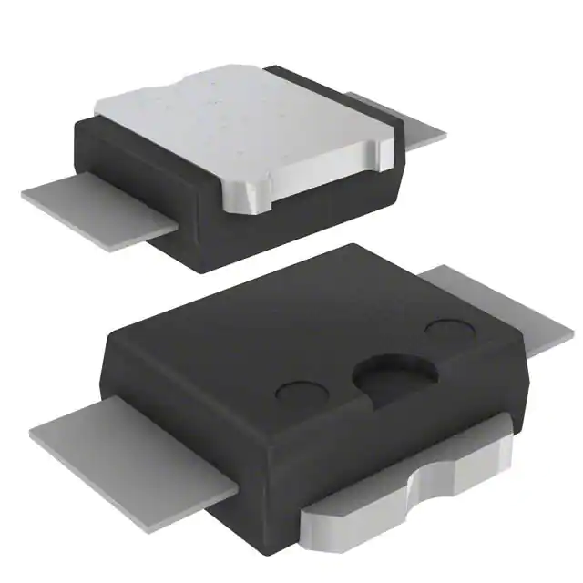
PowerSO-10RF
(formed lead)
The device is a common source N-channel,
enhancement-mode lateral field-effect RF power
MOSFET. It is designed for high gain, broad band
commercial and industrial applications. It operates
at 28 V in common source mode at frequencies
up to 1 GHz. The device boasts the excellent
gain, linearity and reliability of ST’s latest
LDMOS technology mounted in the first true SMD
plastic RF power package, PowerSO-10RF.
Device’s superior linearity performance makes it
an ideal solution for base station applications. The
PowerSO-10 plastic package, designed to offer
high reliability, is the first ST JEDEC
approved, high power SMD package. It has been
specially optmized for RF needs and offers
excellent RF performances and ease of assembly.
Mounting recommendations are available in
www.st.com/rf/ (look for application note AN1294).
PowerSO-10RF
(straight lead)
Figure 1.
Pin connection
Source
Drain
Gate
Table 1.
June 2010
Device summary
Order code
Package
Packing
PD57060-E
PowerSO-10RF (formed lead)
Tube
PD57060S-E
PowerSO-10RF (straight lead)
Tube
PD57060TR-E
PowerSO-10RF (formed lead)
Tape and reel
PD57060STR-E
PowerSO-10RF (straight lead)
Tape and reel
Doc ID 11758 Rev 4
1/21
www.st.com
21
�Contents
PD57060-E
Contents
1
2
Electrical data . . . . . . . . . . . . . . . . . . . . . . . . . . . . . . . . . . . . . . . . . . . . . . 3
1.1
Maximum ratings . . . . . . . . . . . . . . . . . . . . . . . . . . . . . . . . . . . . . . . . . . . . 3
1.2
Thermal data . . . . . . . . . . . . . . . . . . . . . . . . . . . . . . . . . . . . . . . . . . . . . . . 3
Electrical characteristics . . . . . . . . . . . . . . . . . . . . . . . . . . . . . . . . . . . . . 4
2.1
Static . . . . . . . . . . . . . . . . . . . . . . . . . . . . . . . . . . . . . . . . . . . . . . . . . . . . . 4
2.2
Dynamic . . . . . . . . . . . . . . . . . . . . . . . . . . . . . . . . . . . . . . . . . . . . . . . . . . . 4
2.3
Moisture sensitivity level . . . . . . . . . . . . . . . . . . . . . . . . . . . . . . . . . . . . . . . 4
3
Impedances . . . . . . . . . . . . . . . . . . . . . . . . . . . . . . . . . . . . . . . . . . . . . . . . 5
4
Typical performance . . . . . . . . . . . . . . . . . . . . . . . . . . . . . . . . . . . . . . . . . 6
5
Test circuit . . . . . . . . . . . . . . . . . . . . . . . . . . . . . . . . . . . . . . . . . . . . . . . . . 9
6
Common source s-parameter . . . . . . . . . . . . . . . . . . . . . . . . . . . . . . . . 12
7
Package mechanical data . . . . . . . . . . . . . . . . . . . . . . . . . . . . . . . . . . . . 15
8
Revision history . . . . . . . . . . . . . . . . . . . . . . . . . . . . . . . . . . . . . . . . . . . 20
2/21
Doc ID 11758 Rev 4
�PD57060-E
Electrical data
1
Electrical data
1.1
Maximum ratings
Table 2.
Absolute maximum ratings (TCASE = 25°C)
Symbol
Value
Unit
V(BR)DSS
Drain-Source Voltage
65
V
VGS
Gate-Source Voltage
± 20
V
Drain Current
7
A
Power Dissipation (@ Tc = 70°C)
79
W
Max. Operating Junction Temperature
165
°C
-65 to +150
°C
Value
Unit
1.0
°C/W
ID
PDISS
TJ
TSTG
1.2
Parameter
Storage Temperature
Thermal data
Table 3.
Symbol
RthJC
Thermal data
Parameter
Junction - case thermal resistance
Doc ID 11758 Rev 4
3/21
�Electrical characteristics
2
PD57060-E
Electrical characteristics
TCASE = +25 oC
2.1
Static
Table 4.
Static
Symbol
2.2
Test conditions
Max
Unit
VGS = 0
IDS = 1 mA
IDSS
VGS = 0
VDS = 28 V
1
µA
IGSS
VGS = 20 V
VDS = 0 V
1
µA
VGS(Q)
VDS = 28 V
ID = 100 mA
4.0
V
VDS(ON)
VGS = 10 V
ID = 3 A
0.8
V
GFS
VDS = 10 V
ID = 3 A
CISS
VGS = 0
VDS = 28 V
f = 1 MHz
83
pF
COSS
VGS = 0
VDS = 28 V
f = 1 MHz
58
pF
CRSS
VGS = 0
VDS = 28 V
f = 1 MHz
3
pF
65
V
2.0
0.7
2.5
mho
Dynamic
Dynamic
Symbol
Test conditions
Min
Typ
Max
Unit
POUT
VDD = 28 V
IDQ = 100 mA
f = 945MHz
GPS
VDD = 28 V
IDQ = 100 mA POUT = 60 W
f = 945MHz
14.3
dB
ηD
VDD = 28 V
IDQ = 100 mA POUT = 60 W
f = 945MHz
54
%
VDD = 28 V IDQ = 100 mA POUT = 60W
Load
Mismatch All Phase Angles
f = 945MHz
60
5:1
W
VSWR
Moisture sensitivity level
Table 6.
4/21
Typ
V(BR)DSS
Table 5.
2.3
Min
Moisture sensitivity level
Test methodology
Rating
J-STD-020B
MSL 3
Doc ID 11758 Rev 4
�PD57060-E
3
Impedances
Impedances
Figure 2.
Current conventions
Table 7.
Impedance data
Freq. (MHz)
ZIN (Ω)
ZDL(Ω)
890 MHz
0.646 + j 0.694
1.577 - j 0.997
925 MHz
0.568 + j 0.372
1.427 - j 1.459
945 MHz
0.705 + j 0.692
1.278 - j 1.935
960 MHz
0.591 + j 1.039
1.173 - j 2.464
Doc ID 11758 Rev 4
5/21
�Typical performance
PD57060-E
4
Typical performance
Figure 3.
Capacitance vs supply voltage
Figure 4.
C (pF)
Id (A)
1000
8
Drain current vs gate source
voltage
7
6
Ciss
100
5
Coss
4
3
10
Crss
2
1
VDS=10 V
f = 1 MHz
1
0
0
5
10
15
20
25
30
2
2.5
3
3.5
VDS (V)
Figure 5.
4
4.5
5
5.5
6
VGS (V)
Gate-source voltage vs
case temperature
Figure 6.
VGS (Normalized)
Pout (W)
1.06
80
Output power vs input power
945MHz
70
1.04
890MHz
925MHz
60
1.02
960MHz
Id = 5 A
50
1
Id = 4 A
40
Id = 3 A
0.98
30
Id = 2 A
0.96
20
Id = 1 A
Id = 0.5 A
0.94
10
VDS=28V
IDQ=100mA
VDS = 10 V
0.92
0
-25
0
25
50
75
100
0
Tc (°C)
6/21
0.5
1
1.5
2
Pin (W)
Doc ID 11758 Rev 4
2.5
3
3.5
4
�PD57060-E
Figure 7.
Typical performance
Power gain vs output power
Figure 8.
Gp (dB)
Nd (%)
18
70
16
Drain efficiency vs output power
925MHz
890MHz
925MHz
945MHz
945MHz
60
14
960MHz
12
960MHz
890MHz
50
10
40
8
6
30
4
VDS=28V
IDQ=100mA
VDS=28V
IDQ=100mA
2
20
0
10
20
30
40
50
60
70
80
0
10
20
30
Pout (W)
Figure 9.
40
50
60
70
80
Pout (W)
Input return loss vs output power
RL (dB)
Figure 10. Output power vs bias current
Pout (W)
0
80
925MHz
70
890MHz
890MHz
-10
60
960MHz
945MHz
960MHz
50
925MHz
-20
40
945MHz
30
-30
20
Pin=32.8dBm
VDS=28V
VDS=28V
IDQ=100mA
-40
10
0
10
20
30
40
50
60
70
80
0
Pout (W)
0.5
1
1.5
2
2.5
IDQ (A)
Doc ID 11758 Rev 4
7/21
�Typical performance
PD57060-E
Figure 11. Drain efficiency vs bias current
Figure 12. Output power vs supply voltage
Nd (%)
Pout (W)
70
70
945MHz
60
890MHz
60
945MHz
925MHz
890MHz
50
960MHz
50
960MHz
925MHz
40
40
30
30
20
20
Pin=32.8dBm
IDQ=100mA
Pin=32.8dBm
VDS=28V
10
10
0
0.5
1
1.5
2
2.5
10
15
20
IDQ (A)
Figure 13. Drain efficiency vs supply voltage
30
Figure 14. Output power vs gate-source
voltage
Nd (%)
Pout (W)
70
80
925MHz
945MHz
890MHz
60
25
VDS (V)
70
890MHz
60
925MHz
50
9455MHz
960MHz
960MHz
50
40
40
30
30
20
Pin=32.8dBm
VDS=28v
20
Pin=32.8dBm
IDQ=100mA
10
10
10
15
20
25
30
0
VDS (V)
8/21
1
2
3
VGS (V)
Doc ID 11758 Rev 4
4
5
�PD57060-E
5
Test circuit
Test circuit
Figure 15. Test circuit schematic
=* * �
�
5)
,
1
Note:
=' '
�
�
5)
2
很抱歉,暂时无法提供与“PD57060S-E”相匹配的价格&库存,您可以联系我们找货
免费人工找货- 国内价格 香港价格
- 1+577.264651+74.47190
- 10+477.0764610+61.54680
- 50+436.9723850+56.37304
- 100+424.55806100+54.77149
- 国内价格
- 1+623.62440
- 30+604.19520