®
RBO08-40G/T
REVERSED BATTERY AND OVERVOLTAGE PROTECTION
Application Specific Discretes A.S.D.™
FEATURES
s
s
s
s
s
s
s
8A DIODE TO GUARD AGAINST BATTERY REVERSAL. NEGATIVE OVERVOLTAGE PROTECTION BY CLAMPING. COMPLIANT WITH ISO/DTR 7637 STANDARD FOR PULSES 1, 2, 3a and 3b. SUITABLE FOR AUTOPROTECTED ALTERNATOR ENVIRONMENT. BREAKDOWN VOLTAGE : 24 V min. CLAMPING VOLTAGE : ± 40 V max. MONOLITHIC STRUCTURE FOR GREATER RELIABILITY.
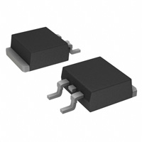
D2PAK RBO08-40G
DESCRIPTION Designed to protect against battery reversal and overvoltages in automotive applications, this monolithic component offers multiple functions in the same package : D1 : reversed battery protection T1 : clamping against negative overvoltages T2 : Transil function for overvoltage protection. TO220-AB RBO08-40T
FUNCTIONAL DIAGRAM
1
3
2
TM : TRANSIL and ASD are trademarks of STMicroelectronics.
October 2003 - Ed: 3
1/9
�RBO08-40G / RBO08-40T
ABSOLUTE MAXIMUM RATINGS Symbol IFSM IF PPP PPP Tstg Tj TL Parameter Non repetitive surge peak forward current (Diode D1) DC forward current (Diode D1) Peak pulse power between Input and Output (Transil T1) see note 1 Tj initial = 25°C tp = 10 ms Tc = 75°C 10/1000 µs Value 80 8 600 1500 - 40 to + 150 150 260 Unit A A W W °C °C
Peak pulse power between Pins 3 and 2 (10/1000µs) Storage temperature range Maximum junction temperature Maximum lead temperature for soldering during 10 s at 4.5mm from case for TO220-AB
Note 1 : for a surge greater than the maximum value, the device will fail in short-circuit..
THERMAL RESISTANCE Symbol Rth (j-c) Junction to case Parameter RBO08-40M RBO08-40T Value 2.4 2.4 Unit °C/W
D1 1 3
I32
I13
IF
Ipp32
T1
2
T2
IR 32 IR M 32
VCL 31 VBR 31 VR M 31 VF 13 IR M 31 IR 31
V13
VR M 32 VB R 32 VC L 32
V32
1
3
Ipp31
2
2/9
�RBO08-40G / RBO08-40T
Symbol VRM31/VRM32 VBR31/VBR32 IR31/IR32 VCL31/VCL32 VF13 IPP αT C31/C32 Parameter Stand-off voltage Transil T1 / Transil T2. Breakdown voltage Transil T1 / Transil T2. Leakage current Transil T1 / Transil T2. Clamping voltage Transil T1 / Transil T2. Forward voltage drop Diode D1. Peak pulse current. Temperature coefficient of VBR. Capacitance Transil T1 / Transil T2. Value Min. RBO08-40G RBO08-40T IF = 8 A @ Tamb = 25°C VF 13 IF = 4 A IF = 4 A @ Tamb = 25°C VF 13 IF = 1 A IF = 1 A @ Tamb = 25°C IF = 1 A @ Tj = 85°C ELECTRICAL CHARACTERISTICS : TRANSIL T1 (- 40°C < Tamb < + 85°C) Symbol VBR 31 VBR 31 IRM 31 IRM 31 VCL 31 αT C 31 IR = 1 mA IR = 1 mA, Tamb = 25°C VRM = 20 V VRM = 20 V, Tamb = 25°C IPP = 15A, Tj initial = 25°C Temperature coefficient of VBR F = 1MHz VR = 0 V 1000 10/1000µs Test Conditions Value Min. 22 24 Typ. Max. 35 32 50 10 40 9 Unit V V µA µA V 10 /°C pF
-4
ELECTRICAL CHARACTERISTICS : DIODE D1 (- 40°C < Tamb < + 85°C) Symbol VF 13 IF = 8 A Test Conditions Typ. Max. 1.5 1.7 1.45 RBO08-40G RBO08-40T 1.3 1.35 1.2 1.1 1.0 0.9 Unit V V V V V V V V V
ELECTRICAL CHARACTERISTICS : TRANSIL T2 (- 40°C < Tamb < + 85°C) Symbol VBR 32 VBR 32 IRM 32 IRM 32 VCL 32 αT IR = 1 mA IR = 1 mA, Tamb = 25°C VRM = 20 V VRM = 20 V, Tamb = 25°C IPP = 37.5 A Temperature coefficient of VBR 10/1000µs Test Conditions Value Min. 22 24 Typ. Max. 35 32 50 10 40 8.5 Unit V V µA µA V 10-4/⊃ C
3/9
�RBO08-40G / RBO08-40T
PRODUCT DESCRIPTION The RBO has 3 functions integrated on the same chip. D1 : “Diode function” in order to protect against reversed battery operation. T2 : “Transil function” in order to protect against positive surge generated by electric systems (ignition, relay. ...). T1 : Protection againt negative surges such as inductive overvoltages (see motor application below).
1
3
2
BASIC APPLICATION * The monolithic multi-function protection (RBO) has been developed to protect sensitive semiconductors in car electronic modules against both overvoltage and battery reverse. * In addition, the RBO circuit prevents overvoltages generated by the module from affecting the car supply network.
MOTOR DRIVER APPLICATION
BATTERY D1 T2 T1 MOTOR
Filter
RBO DEVICE
MOTOR CONTROL
In this application, one half of the motor drive circuit is supplied through the “RBO” and is thus protected as per its basic function application. The second part is connected directly to the “car supply network” and is protected as follows : - For positive surges : T2 (clamping phase) and D1 in forward-biased. - For negative surges : T1 (clamping phase) and T2 in forward-biased.
4/9
�RBO08-40G / RBO08-40T
PINOUT configuration in D2PAK : - Input (1) - Output (3) - Gnd (2) : Pin 1 : Pin 3 : Connected to base Tab
D1
T2
T1 TAB
PINOUT configuration in TO220AB : - Input (1) : Pin 1 - Output (3) : Pin 3 - GND (2) : Connected to base Tab
D1 T2
T1
(TAB)
5/9
�RBO08-40G / RBO08-40T
Fig. 1 : Peak pulse power versus exponential pulse duration (Tj initial = 85°C).
Fig. 2-1 : Clamping voltage versus peak pulse current (Tj initial = 85°C). Exponential waveform tp = 40 ms and tp = 1 ms (TRANSIL T2).
VCL (V) 45 40
Pp p (kW) 10.0 5.0 2.0 1.0 0.5
Diode D1 Transil T2
tp = 40ms
35
tp = 1ms
30
0.2 0.1 tp(ms) 1 2 5 10 20 50 100
25 0.1 0.2 0.5 1.0
Ipp(A) 2.0 5.0 10.0 20.0 50.0
Fig. 2-2 : Clamping voltage versus peak pulse current (Tj initial = 85°C). Exponential waveform tp = 1 ms and tp = 20 µs (TRANSIL T1).
VCL (V) 50
Fig. 3 : Relative variation of peak pulse power versus junction temperature.
Ppp[Tj]/Ppp[Tj initial=85°C]
1.20 1.00 0.80
45 40 35 30 Ipp(A) 25 0.1 0.2 0.5 1.0 2.0 5.0 10.0 20.0 50.0 100.0
tp = 1ms tp = 20µs
0.60 0.40 0.20 Tj initial (°C) 0.00 0 25 50 75 100 125 150 175
6/9
�RBO08-40G / RBO08-40T
Fig. 4 : Relative variation of thermal impedance junction to case versus pulse duration.
Zth(j-c)/Rth(j-c) 1.0
Fig. 5-1 : Peak forward voltage drop versus peak forward current (typical values) - (TRANSIL T2).
VFM(V) 2.0 1.8 1.6 1.4 1.2 1.0 0.8 0.6 0.4 0.2 0.0 0.1
0.5
Tj=25°C
0.2 tp (s) 0.1 1E-3 1E-2 1E-1 1E+0 1E+1
Tj=150°C
IFM (A)
1.0 10.0 20.0
Fig. 5-2 : Peak forward voltage drop versus peak forward current (typical values) - (DIODE D1).
1.6 1.4 1.2 1.0 0.8 0.6 0.4 0.2 0.0 0.1
Tj=150°C Tj=25°C
Fig. 6 : Relative variation of leakage current versus junction temperature.
VFM(V)
IFM (A)
1.0 10.0 20.0
ORDERING INFORMATION
RBO
Reverse Battery & Overvoltage Protection
08
-
40
VCL = 40V
G
IF(AV) = 8A
Package: G = D2PAK T = TO-220AB
7/9
�RBO08-40G / RBO08-40T
PACKAGE MECHANICAL DATA D2PAK Plastic DIMENSIONS REF.
A E L2 C2
Millimeters Min. Typ. Max. Min. 4.60 0.169 2.69 0.098 0.23 0.001 0.93 0.027 1.40 0.45 1.21 8.95 10.00 4.88 15.00 1.27 1.40 0.40 0° 8° 0° 0.60 0.017 1.36 0.047 9.35 0.352 10.28 0.393 5.28 0.192 15.85 0.590 1.40 0.050 1.75 0.055 4.30 2.49 0.03 0.70
Inches Typ. Max. 0.181 0.106 0.009 0.037 0.055 0.024 0.054 0.368 0.405 0.208 0.624 0.055 0.069 0.016 8°
A A1 A2
D
L L3 A1 B2 B G A2 2.0 MIN. FLAT ZONE V2 C R
B B2 C C2 D E G L L2 L3 R V2
FOOT-PRINT D2PAK
16.90
10.30 1.30
5.08
3.70 8.90
8/9
�RBO08-40G / RBO08-40T
PACKAGE MECHANICAL DATA TO-220AB Plastic DIMENSIONS REF. A a1 a2 B b1 b2 C c1 c2 e F I L l2 l3 12.70 10.20 0.64 1.15 4.48 0.35 2.10 2.29 5.85 3.55 2.54 1.45 0.80 Millimeters Min. 14.23 Max. 15.87 4.50 14.70 10.45 0.96 1.39 4.82 0.65 2.70 2.79 6.85 4.00 3.00 1.75 1.20 0.500 0.402 0.025 0.045 0.176 0.020 0.083 0.090 0.230 0.140 0.100 0.057 0.031 Inches Min. 0.560 Max. 0.625 0.177 0.579 0.411 0.038 0.055 0.190 0.026 0.106 0.110 0.270 0.157 0.118 0.069 0.047
Information furnished is believed to be accurate and reliable. However, STMicroelectronics assumes no responsibility for the consequences of use of such information nor for any infringement of patents or other rights of third parties which may result from its use. No license is granted by implication or otherwise under any patent or patent rights of STMicroelectronics. Specifications mentioned in this publication are subject to change without notice. This publication supersedes and replaces all information previously supplied. STMicroelectronics products are not authorized for use as critical components in life support devices or systems without express written approval of STMicroelectronics.
The ST logo is a registered trademark of STMicroelectronics. All other names are the property of their respective owners. © 2003 STMicroelectronics - All rights reserved. STMicroelectronics GROUP OF COMPANIES Australia - Belgium - Brazil - Canada - China - Czech Republic - Finland - France - Germany Hong Kong - India - Israel - Italy - Japan - Malaysia - Malta - Morocco - Singapore - Spain Sweden - Switzerland - United Kingdom - United States www.st.com 9/9
�
很抱歉,暂时无法提供与“RBO08-40G”相匹配的价格&库存,您可以联系我们找货
免费人工找货