SCTWA90N65G2V-4
Datasheet
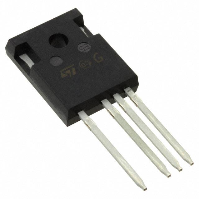
Silicon carbide Power MOSFET 650 V, 18 mΩ typ., 119 A in an HiP247-4 package
Features
1
2
4
3
HiP247-4
Order code
VDS
RDS(on) max.
ID
SCTWA90N65G2V-4
650 V
24 mΩ
119 A
•
•
High speed switching performance
Very high operating junction temperature capability (TJ = 200 °C)
•
•
•
Very fast and robust intrinsic body diode
Extremely low gate charge and input capacitances
Source sensing pin for increased efficiency
Drain(1, TAB)
Applications
•
•
•
Gate(4)
Driver
source(3)
Power
source(2)
ND1TPS2DS3G4
Switching mode power supply
DC-DC converters
Industrial motor control
Description
This silicon carbide Power MOSFET device has been developed using ST’s
advanced and innovative 2nd generation SiC MOSFET technology. The device
features remarkably low on-resistance per unit area and very good switching
performance. The variation of switching loss is almost independent of junction
temperature.
Product status link
SCTWA90N65G2V-4
Product summary
Order code
SCTWA90N65G2V-4
Marking
SCT90N65G2V
Package
HiP247-4
Packing
Tube
DS13582 - Rev 1 - November 2020
For further information contact your local STMicroelectronics sales office.
www.st.com
�SCTWA90N65G2V-4
Electrical ratings
1
Electrical ratings
Table 1. Absolute maximum ratings
Symbol
VDS
VGS
Parameter
Value
Unit
Drain-source voltage
650
V
Gate-source voltage
-10 to 22
Gate-source voltage (recommended operating values)
-5 to 18
V
Drain current (continuous) at TC = 25 °C
119
Drain current (continuous) at TC = 100 °C
90
IDM (1)
Drain current (pulsed)
220
A
PTOT
Total power dissipation at TC = 25 °C
565
W
Tstg
Storage temperature range
ID
Tj
Operating junction temperature range
-55 to 200
A
°C
°C
1. Pulse width is limited by safe operating area.
Table 2. Thermal data
Symbol
DS13582 - Rev 1
Parameter
RthJC
Thermal resistance, junction-to-case
RthJA
Thermal resistance, junction-to-ambient
Value
Unit
0.31
°C/W
40
°C/W
page 2/13
�SCTWA90N65G2V-4
Electrical characteristics
2
Electrical characteristics
(TCASE = 25 °C unless otherwise specified).
Table 3. On/off states
Symbol
Parameter
Test conditions
Drain-source breakdown
voltage
VGS = 0 V, ID = 1 mA
IDSS
Zero gate voltage drain
current
VDS = 650 V, VGS = 0 V
IGSS
Gate-body leakage current
VDS = 0 V, VGS = -10 to 22 V
VGS(th)
Gate threshold voltage
VDS = VGS, ID = 1 mA
RDS(on)
Static drain-source onresistance
V(BR)DSS
Min.
Typ.
Max.
650
Unit
V
10
µA
±100
nA
3.2
5.0
V
VGS = 18 V, ID = 50 A
18
24
VGS = 18 V, ID = 50 A, TJ = 200 °C
30
1.9
mΩ
Table 4. Dynamic, based on HiP247 package option
Symbol
Parameter
Ciss
Input capacitance
Coss
Output capacitance
Crss
Reverse transfer capacitance
Qg
Total gate charge
Qgs
Gate-source charge
Qgd
Gate-drain charge
Rg
Gate input resistance
Test conditions
VDS = 400 V, f = 1 MHz, VGS = 0 V
VDD = 400 V, ID = 50 A,
VGS = -5 V to 18 V
f = 1 MHz, ID = 0 A
Min.
Typ.
Max.
Unit
-
3380
-
-
294
-
-
49
-
-
157
-
-
43
-
-
42
-
-
1
-
Ω
Unit
pF
nC
Table 5. Switching energy (inductive load), based on HiP247 package option
Symbol
DS13582 - Rev 1
Parameter
Eon
Turn-on switching energy
Eoff
Turn-off switching energy
Eon
Turn-on switching energy
Eoff
Turn-off switching energy
Test conditions
VDD = 400 V, ID = 50 A, RG = 2.2 Ω,
VGS = -5 to 18 V
VDD = 400 V, ID = 50 A, RG = 2.2 Ω,
VGS = -5 to 18 V, TJ= 200 °C
Min.
Typ.
Max.
-
130
-
-
210
-
-
135
-
-
200
-
µJ
page 3/13
�SCTWA90N65G2V-4
Electrical characteristics
Table 6. Switching times, based on HiP247 package option
Symbol
td(on)
tf
td(off)
tr
Parameter
Test conditions
Turn-on delay time
Min.
Typ.
Max.
-
26
-
Fall time
VDD = 400 V, ID = 50 A,
-
16
-
Turn-off delay time
RG = 2.2 Ω, VGS = -5 V to 18 V,
-
58
-
-
38
-
Rise time
Unit
ns
Table 7. Reverse SiC diode characteristics, based on HiP247 package option
Symbol
VSD
DS13582 - Rev 1
Parameter
Test conditions
Min.
Typ.
Max.
Unit
Forward on voltage
IF = 30 A, VGS = 0 V
-
2.5
-
V
trr
Reverse recovery time
IF = 50 A, di/dt = 4000 A/µs,
-
17
-
ns
Qrr
Reverse recovery charge
VGS = VGS = -5 V to 18 V,
-
308
-
nC
IRRM
Reverse recovery current
VDD = 400 V, TJ = 25 °C
-
30
-
A
page 4/13
�SCTWA90N65G2V-4
Electrical characteristics (curves), based on HiP247 package option
2.1
Electrical characteristics (curves), based on HiP247 package option
Figure 1. Safe operating area
ID
(A)
Figure 2. Maximum transient thermal impedance
ZthJ-C
(°C/W)
GADG110720191006SOA
IDM
n)
tp =10µs
DS
(o
O
is per
lim ati
ite on
d in
by th
R is a
10 2
re
a
10-1
10 1
V(BR)DSS
tp =100µs
RDS(on) max.
tp =1ms
TC = 25 °C
TJ ≤ 200°C
single pulse
10 0
10 1
10 0
10 -1
10
VDS (V)
2
GADG110720191014OCH_-50
VGS =12V
60
RthJ-C = 0.31 (°C/W)
duty = ton / T
Single pulse
10-4
10-6
T
10-5
10-4
10-3
10-2
10-1
tp (s)
Figure 4. Typical output characteristics (TJ = 25 °C)
GADG120720191341OCH_25
VGS =16, 18, 20V
VGS =14V
VGS =12V
80
VGS =10V
60
40
40
VGS =10V
20
1
2
3
4
5
6
VGS = 8V
VDS (V)
Figure 5. Typical output characteristics (TJ = 200 °C)
VGS =14,16,18, 20V
120
80
0
0
1
2
3
4
5
6
VGS =6V
VDS (V)
Figure 6. Typical transfer characteristics
GADG110720191016TCH
120
VGS =12V
VGS =10V
VGS =8V
100
VGS =8V
20
ID
(A)
GADG110720191015OCH_200
ID
(A)
VDS = 3 V
100
80
60
60
TJ = 200 °C
TJ = 25 °C
40
40
VGS =6V
20
DS13582 - Rev 1
0.01
100
VGS =14V
80
0
0
0.02
120
VGS =16V
100
0
0
0.2
0.1
0.05
ton
ID
(A)
VGS = 18, 20V
120
10-3
duty=0.5
tp =10ms
Figure 3. Typical output characteristics (TJ = -50 °C)
ID
(A)
10-2
GADG110720191010ZTH
1
2
3
4
5
6
VDS (V)
20
0
0
4
8
12
16
VGS (V)
page 5/13
�SCTWA90N65G2V-4
Electrical characteristics (curves), based on HiP247 package option
Figure 7. Typical capacitances
C
(pF)
Figure 8. Typical gate charge
VGS
(V)
GADG110720191017CVR
CISS
15
GADG110720191018QVG
VDD = 400 V
ID = 50 A
10 3
10
COSS
5
10 2
f = 1 MHz
CRSS
10 1
10 -1
10 0
10 1
10 2
VDS (V)
Figure 9. Maximum total power dissipation
PTOT
(W)
GADG110720191023PDT
0
-5
0
400
19
200
17
100
16
25
75
125
175
TC (°C)
Figure 11. Normalized on-resistance vs temperature
RDS(on)
(norm.)
GADG110720191026RON
1.8
Qg (nC)
GADG110720191025RID
VGS = 18 V
15
0
20
40
60
80
100
ID (A)
Figure 12. Normalized gate threshold voltage vs
temperature
VGS(th)
(norm.)
GADG110720191027VTH
1.4
1.2
1.4
ID = 250 µA
1.0
1.2
0.8
1.0
DS13582 - Rev 1
150
VGS = 18 V
1.6
0.8
-75
120
18
TJ =200 °C
-25
90
RDS(on)
(mΩ)
20
0
-75
60
Figure 10. Typical drain-source on-resistance
500
300
30
0.6
-25
25
75
125
175
TJ (°C)
0.4
-75
-25
25
75
125
175
TJ (°C)
page 6/13
�SCTWA90N65G2V-4
Electrical characteristics (curves), based on HiP247 package option
Figure 13. Normalized breakdown voltage vs temperature
V(BR)DSS
(norm.)
GADG110720191027BDV
1.06
E
(µJ) VDD = 400 V
VGS = -5 to 18 V
600 R = 2.2 Ω
G
GADG110720191040SDC
Etot
500
ID = 1 mA
1.04
Figure 14. Typical switching energy vs drain current
Eoff
400
1.02
300
1.00
0.98
100
0.96
-75
-25
25
75
125
175
TJ (°C)
Figure 15. Typical switching energy vs temperature
GADG110720191041SLT
E
(µJ) VDD = 400 V, ID = 50 A,
VGS = -5 to 18 V, RG = 2.2 Ω
360
E
tot
300
0
20
180
50
60
70
ID (A)
GADG110720191046RCC_-50
ID
(A)
-20
-60
Eon
-80
VGS =-3, -5V
-100
60
-120
0
-25
25
75
125
175
TC (°C)
Figure 17. Typical reverse conduction characteristics
(TJ = 25 °C)
GADG110720191043RCC_25
ID
(A)
-20
-140
-6
VGS =0V
VGS =5V
VGS =10V
-5
-4
-3
VGS =15V
-2
-1
VDS (V)
Figure 18. Typical reverse conduction characteristics
(TJ = 150 °C)
GADG110720191048RCC_150
ID
(A)
-20
VGS =-5, -3V
-40
-60
-60
-80
-80
-100
VGS =15V
VGS =0V
VGS =5V
-120
DS13582 - Rev 1
40
Figure 16. Typical reverse conduction characteristics
(TJ = -50 °C)
Eoff
120
-140
-6
30
-40
240
-40
Eon
200
-5
-4
-3
-1
-100
VGS =0V
VGS =5V
-120
VGS =10V
-2
VGS =-3, -5V
VDS (V)
-140
-6
VGS =15V
VGS =10V
-5
-4
-3
-2
-1
VDS (V)
page 7/13
�SCTWA90N65G2V-4
Test circuits
3
Test circuits
Figure 19. Switching times test circuit for resistive load
Figure 20. Test circuit for gate charge behavior
VDD
12V
47kΩ
1kΩ
100nF
+
VD
VGS
3.3
µF
2200
RL
µF
IG=CONST
VDD
2200
µF
+
RG
100Ω
Vi ≤ VGS
D.U.T.
D.U.T.
VG
2.7kΩ
PW
47kΩ
GND1
(driver signal)
GND2
(power)
1kΩ
PW
GND1
AM15855v1
Figure 21. Test circuit for inductive load switching and
diode recovery times
A
A
D.U.T.
FAST
DIODE
S
A
L
L=100µH
D
25Ω
VD
3.3
µF
B
B
B
AM15856v1
Figure 22. Unclamped inductive load test circuit
D
G
GND2
+
1000
µF
2200
µF
+
VDD
3.3
µF
VDD
ID
G
S
RG
D.U.T.
Vi
Pw
GND2
GND1
D.U.T.
GND1
GND2
AM15858v1
AM15857v1
Figure 24. Switching time waveform
Figure 23. Unclamped inductive waveform
ton
td(on)
V(BR)DSS
toff
td(off)
tr
tf
VD
90%
90%
IDM
ID
VDD
10%
0
VDS
10%
VDD
VGS
AM01472v1
0
90%
10%
AM01473v1
DS13582 - Rev 1
page 8/13
�SCTWA90N65G2V-4
Package information
4
Package information
In order to meet environmental requirements, ST offers these devices in different grades of ECOPACK packages,
depending on their level of environmental compliance. ECOPACK specifications, grade definitions and product
status are available at: www.st.com. ECOPACK is an ST trademark.
4.1
HiP247-4 package information
Figure 25. HiP247-4 package outline
8405626_2
DS13582 - Rev 1
page 9/13
�SCTWA90N65G2V-4
HiP247-4 package information
Table 8. HiP247-4 mechanical data
Dim.
mm
Min.
Typ.
Max.
A
4.90
5.00
5.10
A1
2.31
2.41
2.51
A2
1.90
2.00
2.10
b
1.16
b1
1.15
b2
0
0.20
c
0.59
0.66
c1
0.58
0.60
0.62
D
20.90
21.00
21.10
D1
16.25
16.55
16.85
D2
1.05
1.20
1.35
D3
24.97
25.12
25.27
E
15.70
15.80
15.90
E1
13.10
13.30
13.50
E2
4.90
5.00
5.10
E3
2.40
2.50
2.60
e
2.44
2.54
2.64
e1
4.98
5.08
5.18
L
19.80
19.92
20.10
P
3.50
3.60
3.70
1.29
1.20
P1
7.40
P2
2.40
Q
5.60
S
DS13582 - Rev 1
1.25
2.50
2.60
6.00
6.15
T
9.80
10.20
U
6.00
6.40
page 10/13
�SCTWA90N65G2V-4
Revision history
Table 9. Document revision history
DS13582 - Rev 1
Date
Revision
25-Nov-2020
1
Changes
First release.
page 11/13
�SCTWA90N65G2V-4
Contents
Contents
1
Electrical ratings . . . . . . . . . . . . . . . . . . . . . . . . . . . . . . . . . . . . . . . . . . . . . . . . . . . . . . . . . . . . . . . . . .2
2
Electrical characteristics. . . . . . . . . . . . . . . . . . . . . . . . . . . . . . . . . . . . . . . . . . . . . . . . . . . . . . . . . . . 3
2.1
Electrical characteristics (curves), based on HiP247 package option . . . . . . . . . . . . . . . . . . . 5
3
Test circuits . . . . . . . . . . . . . . . . . . . . . . . . . . . . . . . . . . . . . . . . . . . . . . . . . . . . . . . . . . . . . . . . . . . . . . .8
4
Package information. . . . . . . . . . . . . . . . . . . . . . . . . . . . . . . . . . . . . . . . . . . . . . . . . . . . . . . . . . . . . . . 9
4.1
HiP247-4 package information . . . . . . . . . . . . . . . . . . . . . . . . . . . . . . . . . . . . . . . . . . . . . . . . . . . 9
Revision history . . . . . . . . . . . . . . . . . . . . . . . . . . . . . . . . . . . . . . . . . . . . . . . . . . . . . . . . . . . . . . . . . . . . . . .11
DS13582 - Rev 1
page 12/13
�SCTWA90N65G2V-4
IMPORTANT NOTICE – PLEASE READ CAREFULLY
STMicroelectronics NV and its subsidiaries (“ST”) reserve the right to make changes, corrections, enhancements, modifications, and improvements to ST
products and/or to this document at any time without notice. Purchasers should obtain the latest relevant information on ST products before placing orders. ST
products are sold pursuant to ST’s terms and conditions of sale in place at the time of order acknowledgement.
Purchasers are solely responsible for the choice, selection, and use of ST products and ST assumes no liability for application assistance or the design of
Purchasers’ products.
No license, express or implied, to any intellectual property right is granted by ST herein.
Resale of ST products with provisions different from the information set forth herein shall void any warranty granted by ST for such product.
ST and the ST logo are trademarks of ST. For additional information about ST trademarks, please refer to www.st.com/trademarks. All other product or service
names are the property of their respective owners.
Information in this document supersedes and replaces information previously supplied in any prior versions of this document.
© 2020 STMicroelectronics – All rights reserved
DS13582 - Rev 1
page 13/13
�