SD1274-01
RF POWER BIPOLAR TRANSISTORS VHF MOBILE APPLICATIONS
FEATURES SUMMARY ■ 160 MHz
■ ■ ■
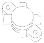
Figure 1. Package
13.6 VOLTS COMMON EMITTER POUT = 30 W MIN. WITH 10 dB GAIN
DESCRIPTION The SD1274-01 is a 13.6 V Class C epitaxial silicon NPN planar transistor designed primarily for VHF communications. The SD1274-01 utilizes an emitter ballasted die geometry to withstand severe load mismatch conditions.
.380 4L FL (M113) epoxy sealed
Figure 2. Pin Connection
1. Collector 2. Emitter
3. Base 4. Emitter
Table 1. Order Codes
Order Codes SD1274-01 Marking SD1274-01 Package M113 Packaging PLASTIC TRAYS
REV. 2 May 2004 1/7
�SD1274-01
Table 2. Absolute Maximum Ratings (Tcase = 25°C)
Symbol VCBO VCEO VCES VEBO IC PDISS TJ TSTG Parameter Collector-Base Voltage Collector-Emitter Voltage Collector-Emitter Voltage Emitter-Base Voltage Device Current Power Dissipation Junction Temperature Storage Temperature Value 36 16 36 4.0 8.0 70 +200 – 65 to +150 Unit V V V V A W °C °C
Table 3. Thermal Data
Symbol RTH(j-c) Parameter Junction-Case Thermal Resistance Value 1.2 Unit °C/W
ELECTRICAL SPECIFICATIONS (TCASE = 25°C) Table 4. Static
Value Symbol BVCES BVCEO BVEBO ICBO hFE Test Conditions Min. IC = 15 mA; VBE = 0 mA IC = 50 mA; IB = 0 mA IE = 5 mA; IC = 0 mA VCB = 15 V; IE = 0 mA VCE = 5 V; IC = 250 mA 36 16 4.0 — 20 Typ. — — — — — Max. — — — 5 — V V V mA — Unit
Table 5. Dynamic
Value Symbol POUT GP COB Test Conditions Min. f = 160 MHz; PIN = 3.0 W; VCE = 13.6 V f = 160 MHz; PIN = 3.0 W; VCE = 13.6 V f = 1 MHz; VCB = 15 V 30 10 — Typ. — — 95 Max. — — — W dB pF Unit
2/7
�SD1274-01
TYPICAL PERFORMANCE Figure 3. Power Output vs Supply Voltage (136 MHz)
Output Power vs. Supply Voltage F = 136 MHz
60 60
Figure 4. Power Output vs Supply Voltage (150 MHz)
Output Power vs. Supply Voltage F = 150 MHz
Pout Output Power (watts)
40
Pin = 2.0 W Pin = 1.5 W
Pout Output Power (watts)
50
50
40
Pin = 2.0 W Pin = 1.5 W
30
30
Pin = 1.0 W
20
20
Pin = 1.0 W
10
10
8
10
12
14
16
18
20
8
10
12
14
16
18
20
Vcc Supply Voltage (volts)
Vcc Supply Voltage (volts)
Figure 5. Power Output vs Supply Voltage (175 MHz)
Output Power vs. Supply Voltage F = 175 MHz
Figure 6. Power Gain vs Frequency
Power Gain vs. Frequency
12
60 10
Pout Output Power (watts)
Power Gain (dB)
50
40
Pin = 3.0 W
8
6
30
Pin = 2.0 W Pin = 1.5 W
4
20 2 10 130 8 10 12 14 16 18 20 140 150 160 170
Pout = 30W Vcc = 13.6V
180 200
Frequency (MHz)
Vcc Supply Voltage (volts)
3/7
�SD1274-01
Figure 7. Power Output vs Power Input
Output Power vs. Input Power
60
Pout Output Power (watts)
50
40
f=136MHz f=150MHz f=175MHz
30
20
10
Vcc = 13.6V
0.25 0.5 1.0 1.5 2.0 2.5 3.0
Pin Input Power (watts)
Table 6. Impedance Data (1)
FREQ. 175 MHz
Note: 1. PIN = 3.0 W; VCE = 12.5 V
ZIN (Ω) 1.0 + j 0.4
ZCL (Ω) 2.3 + j 0.1
4/7
�SD1274-01
PACKAGE MECHANICAL Table 7. M113 Mechanical Data
millimeters Symbol Min A B C D E F G H I J 6.10 0.10 2.16 4.06 5.59 19.94 18.29 24.64 18.54 24.89 9.78 0.15 2.67 4.57 7.11 6.48 0.240 0.004 0.085 0.160 Typ Max 5.84 Min 0.220 0.785 0.720 0.970 0.730 0.980 0.385 0.006 0.105 0.180 0.280 0.255 Typ Max 0.230 inches
Figure 8. M113 Package Dimensions
Note: Drawing is not to scale.
5/7
�SD1274-01
REVISION HISTORY Table 8. Revision History
Date June-1993 24-May-2004 Revision 1 2 First Issue Stylesheet update. No content change. Description of Changes
6/7
�SD1274-01
Information furnished is believed to be accurate and reliable. However, STMicroelectronics assumes no responsibility for the consequences of use of such information nor for any infringement of patents or other rights of third parties which may result from its use. No license is granted by implication or otherwise under any patent or patent rights of STMicroelectronics. Specifications mentioned in this publication are subject to change without notice. This publication supersedes and replaces all information previously supplied. STMicroelectronics products are not authorized for use as critical components in life support devices or systems without express written approval of STMicroelectronics. The ST logo is a registered trademark of STMicroelectronics. All other names are the property of their respective owners © 2004 STMicroelectronics - All rights reserved STMicroelectronics GROUP OF COMPANIES Australia - Belgium - Brazil - Canada - China - Czech Republic - Finland - France - Germany - Hong Kong - India - Israel - Italy - Japan Malaysia - Malta - Morocco - Singapore - Spain - Sweden - Switzerland - United Kingdom - United States www.st.com
7/7
�
很抱歉,暂时无法提供与“SD1274-01”相匹配的价格&库存,您可以联系我们找货
免费人工找货