物料型号:
- 型号:SD2918
- 品牌:无明确品牌标识,但从文档来源看,可能与华强芯城有关
- 订购代码:SD2918
器件简介:
- SD2918是一款金镀层N沟道MOS场效应射频功率晶体管,适用于50V DC大型信号应用,频率范围可达200MHz。
引脚分配:
- 1. Drain(漏极)
- 2. Source(源极)
- 3. Gate(栅极)
- 4. Source(源极)
参数特性:
- 绝对最大额定值:包括漏源电压(125V)、漏栅电压(125V)、栅源电压(±20V)、漏电流(6A)和功耗(175W)等。
- 热阻:包括结壳热阻(0.30°C/W)和结散热器热阻(1.0°C/W)。
功能详解:
- 该晶体管在30MHz频率下,VDD=50V时,可以实现至少30W的输出功率和至少18dB的增益。
- 动态参数包括输出功率、功率增益、漏极效率和负载失配等。
应用信息:
- 适用于30MHz频率下,VDD=50V的射频功率放大应用,可以实现高效率和高增益。
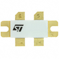
封装信息:
- 封装类型:M113,直径约为0.380英寸,带有旗帜的N/HERM封装。
- 机械尺寸数据以毫米和英寸为单位提供,包括最小、典型和最大值。