SD2931-10
RF power transistor:
HF/VHF/UHF N-channel power MOSFETs
Datasheet - production data
• POUT = 150 W min. with 14 dB gain @ 175 MHz
• Thermally enhanced packaging for lower
junction temperatures
Description
The SD2931-10 is a gold metalized N-channel
MOS field-effect RF power transistor. Being
electrically identical to the standard SD2931
MOSFET, it is intended for use in 50 V dc large
signal applications up to 230 MHz.
M174
Epoxy sealed
The SD2931-10 is mechanical compatible to the
SD2931 but offers in addition a better thermal
capability (25% lower thermal resistance),
representing the best-in-class transistors for ISM
applications, where reliability and ruggedness are
critical factors.
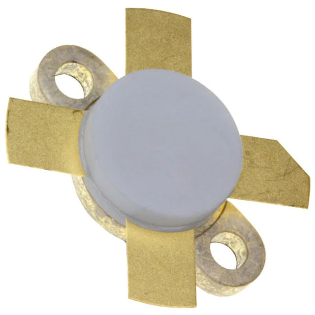
Figure 1. Pin connection
4
1
3
2
1. Drain
3. Gate
2. Source
4. Source
Features
• Gold metalization
• Excellent thermal stability
• Common source configuration
Table 1. Device summary
Order code
Marking
Base qty.
Package
Packaging(1)
SD2931-10W
SD2931-10
25 pcs
M174
Plastic tray
1. For more details please refer to Chapter 11: Marking, packing and shipping specifications.
July 2016
This is information on a product in full production.
DocID7076 Rev 10
1/19
www.st.com
�Contents
SD2931-10
Contents
1
2
Electrical data . . . . . . . . . . . . . . . . . . . . . . . . . . . . . . . . . . . . . . . . . . . . . . 3
1.1
Maximum ratings . . . . . . . . . . . . . . . . . . . . . . . . . . . . . . . . . . . . . . . . . . . . 3
1.2
Thermal data . . . . . . . . . . . . . . . . . . . . . . . . . . . . . . . . . . . . . . . . . . . . . . . 3
Electrical characteristics . . . . . . . . . . . . . . . . . . . . . . . . . . . . . . . . . . . . . 4
2.1
Static . . . . . . . . . . . . . . . . . . . . . . . . . . . . . . . . . . . . . . . . . . . . . . . . . . . . . . 4
2.2
Dynamic . . . . . . . . . . . . . . . . . . . . . . . . . . . . . . . . . . . . . . . . . . . . . . . . . . . 4
3
Transient thermal impedance . . . . . . . . . . . . . . . . . . . . . . . . . . . . . . . . . . 6
4
Impedance data . . . . . . . . . . . . . . . . . . . . . . . . . . . . . . . . . . . . . . . . . . . . . 8
5
Typical performance . . . . . . . . . . . . . . . . . . . . . . . . . . . . . . . . . . . . . . . . . 9
6
Typical performance @ 175 MHz . . . . . . . . . . . . . . . . . . . . . . . . . . . . . . 10
7
Test circuit . . . . . . . . . . . . . . . . . . . . . . . . . . . . . . . . . . . . . . . . . . . . . . . . 11
8
Typical performance @ 30 MHz . . . . . . . . . . . . . . . . . . . . . . . . . . . . . . . 13
9
Test circuit @ 30 MHz . . . . . . . . . . . . . . . . . . . . . . . . . . . . . . . . . . . . . . . 14
10
Package information . . . . . . . . . . . . . . . . . . . . . . . . . . . . . . . . . . . . . . . . 15
11
Marking, packing and shipping specifications . . . . . . . . . . . . . . . . . . . 17
12
Revision history . . . . . . . . . . . . . . . . . . . . . . . . . . . . . . . . . . . . . . . . . . . 18
2/19
DocID7076 Rev 10
�SD2931-10
Electrical data
1
Electrical data
1.1
Maximum ratings
(TCASE = 25 °C).
Table 2. Absolute maximum ratings
Symbol
V(BR)DSS(1)
VDGR
VGS
ID
PDISS
TJ
TSTG
Parameter
Value
Unit
Drain source voltage
125
V
Drain-gate voltage (RGS = 1 MΩ)
125
V
Gate-source voltage
±40
V
Drain current
20
A
Power dissipation
389
W
Max. operating junction temperature
200
°C
-65 to +150
°C
Value
Unit
0.45
°C/W
Storage temperature
1. TJ = 150°C
1.2
Thermal data
Table 3. Thermal data
Symbol
RthJC
Parameter
Junction - case thermal resistance
DocID7076 Rev 10
3/19
19
�Electrical characteristics
2
SD2931-10
Electrical characteristics
(TCASE = 25 °C).
2.1
Static
Table 4. Static (per side)
Symbol
Test conditions
Min
125
Typ
Max
Unit
V(BR)DSS
VGS = 0
IDS = 100 mA
IDSS
VGS = 0
VDS = 50 V
50
μA
VGS = 20
VDS = 0
250
nA
IGSS
VGS(Q)
(1)
VDS = 10 V
ID = 250 mA
VDS(ON)
VGS = 10 V
ID = 10 A
GFS
VDS = 10 V
ID = 5 A
CISS
VGS = 0
VDS = 50 V
COSS
VGS = 0
CRSS
VGS = 0
V
See table below
3.0
5
V
V
6
mho
f = 1 MHz
480
pF
VDS = 50 V
f = 1 MHz
190
pF
VDS = 50 V
f = 1 MHz
18
pF
1. VGS(Q) sorted with alpha/numeric code marked on unit.
2.2
Dynamic
Table 5. Dynamic
Symbol
Test conditions
IDQ = 250 mA
Min
Max
Unit
POUT
VDD = 50 V
f = 175 MHz
150
GPS
VDD = 50 V IDQ = 250 mA POUT = 150 W f = 175 MHz
14
15
dB
nD
VDD = 50 V IDQ = 250 mA POUT = 150 W f = 175 MHz
55
65
%
VDD = 50 V IDQ = 250 mA POUT = 150 W f = 175 MHz
Load
mismatch All phase angles
4/19
Typ
DocID7076 Rev 10
10:1
W
VSWR
�SD2931-10
Electrical characteristics
Table 6. VGS sorts
Symbol
Value
Symbol
Value
A
2.0 - 2.1
K
2.9 - 3.0
B
2.1 - 2.2
L
3.0 - 3.1
C
2.2 - 2.3
M
3.1 - 3.2
D
2.3 - 2.4
N
3.2 - 3.3
E
2.4 - 2.5
P
3.3 - 3.4
F
2.5 - 2.6
Q
3.4 - 3.5
G
2.6 - 2.7
R
3.5 - 3.6
H
2.7 - 2.8
S
3.6 - 3.7
J
2.8 - 2.9
DocID7076 Rev 10
5/19
19
�Transient thermal impedance
3
SD2931-10
Transient thermal impedance
Figure 2. Transient thermal impedance
6LQJOH���UHSHWLWLYH�SXOVH
7KHUPDO�LPSHGDQFH� �=7+- � &���&���:�
����
VLQJOH�SXOVH
���
����
���
����
���
���
����
���
���
����
���
���
����
���
����
����
����
����
����
��(���
��(���
��(���
��(���
��(���
5HFWDQJXODU�SRZHU�SXOVH�ZLGWK��VHF�
6/19
DocID7076 Rev 10
��(���
$0�����9�
�SD2931-10
Transient thermal impedance
Figure 3. Transient thermal impedance model
'LVVLSDWHG3RZHUB:DWWV
5�
5 ������2KP
&
&�
& �������� �)
5
5�
5 �����2KP
&
&�
& �������� �)
5
5�
5 �����2KP
&
&�
& �������� �)
5
5�
5 �����2KP
&
&�
& �������� �)
$0�����9�
DocID7076 Rev 10
7/19
19
�Impedance data
4
SD2931-10
Impedance data
Figure 4. Impedance data
D
ZDL
Typical Input
Impedance
Typical Drain
Load Impedance
G
Zin
S
Table 7. Impedance data
8/19
Freq
ZIN (Ω)
ZDL (Ω)
30 MHz
1.7 - j 5.7
6.8 + j 0.9
175 MHz
1.2 - j 2.0
2.0 + j 2.4
DocID7076 Rev 10
�SD2931-10
5
Typical performance
Typical performance
Figure 5. Capacitance vs drain-source voltage
Figure 6. Drain current vs gate voltage
10000
20
ID, DRAIN CURRENT (A)
C, CAPACITANCE (pF)
Tc=-20 °C
f =1MHz
1000
Ciss
Coss
100
Tc=+25 °C
15
10
Tc=+80 °C
VDS = 10 V
5
Crss
0
10
0
10
20
30
40
2
50
2.5
3
VDS, DRAIN-SOURCE VOLTAGE (V)
Figure 7. Gate-source voltage vs case
temperature
4
4.5
5
5.5
6
Figure 8. Maximum thermal resistance vs case
temperature
1.12
0.6
Id =9A
1.08
Id =10A
Id =7A
Id =5A
1.04
Id =11A
1
0.96
Id =4A
Id =2A
0.92
Id =1A
0.88
RTH(j-c) (°C/W)
VGS, GATE-SOURCE VOLTAGE (NORMALIZED)
3.5
VGS, GATE-SOURCE VOLTAGE (V)
0.56
0.52
0.48
Id =.25A
Vds= 10 V
0.84
Id =.1A
0.44
25
0.8
-25
0
25
50
75
100
35
45
55
65
75
85
Tc, CASE TEMPERATURE (°C)
Tc, CASE TEMPERATURE (°C)
Figure 9. Safe operating area
Ids(A)
100
10
(1)
1
1
10
100
1000
Vds(V)
(1) Current in this area may be limited by Rds(on)
DocID7076 Rev 10
9/19
19
�Typical performance @ 175 MHz
6
SD2931-10
Typical performance @ 175 MHz
Figure 10. Output power vs input power
Figure 11. Output power vs input power
270
240
Pout, OUTPUT POWER (W)
Pout, OUTPUT POWER (W)
270
Vdd= 50V
210
180
Vdd= 40V
150
120
90
60
f= 175MHz
Idq= 250mA
30
0
0
5
10
15
20
180
Tc =+80 °C
150
120
90
Vdd= 50V
Idq= 250mA
f= 175MHz
60
30
0
25
0
5
10
16
70
Nd, EFFICIENCY (%)
80
14
12
10
Vdd=50V
Idq=250mA
f=175Mhz
25
60
50
40
Vdd=50V
Idq=250mA
f=175Mhz
30
6
20
0
50
100
150
200
250
0
50
100
Pout, OUTPUT POWER (W)
150
200
250
Pout, OUTPUT POWER (W)
Figure 14. Output power vs supply voltage
Figure 15. Drain current vs gate-source voltage
270
20
Pin =10W
240
Tc=-20 °C
ID, DRAIN CURRENT (A)
Pout,OUTPUT POWER(W)
20
Figure 13. Efficiency vs output power
18
210
Pin =5W
180
150
Pin =2.5W
120
90
60
Tc=+25 °C
15
10
Tc=+80 °C
5
Idq= 250mA
f= 175MHz
30
0
0
24
28
32
36
40
44
48
52
2
2.5
3
3.5
4
4.5
5
VGS, GATE-SOURCE VOLTAGE (V)
Vdd,DRAIN VOLTAGE(V)
10/19
15
Pin, INPUT POWER(W)
Figure 12. Power gain vs output power
Gp, POWER GAIN (dB)
Tc =+25 °C
210
Pin, INPUT POWER (W)
8
Tc =-20 °C
240
DocID7076 Rev 10
5.5
6
�SD2931-10
7
Test circuit
Test circuit
Figure 16. 175 MHz schematic (production test circuit)
Note: All dimensions in inches
REF. 1021579C
Table 8. Component part list
Component
Description
T1
4:1 transformer, 25 ohm flexible coax .090 OD 6” long
T2
1:4 transformer, 25 ohm semi-rigid coax .141 OD 6” long
FB1
Toroid X 2, 0.5” OD .312” ID 850μ 2 turns
FB2, FB3
VK200
FB4
Shield bead, 1” OD 0.5” ID 850μ 3 turns
L1
1/4 wave choke, 50 ohm semi-rigid coax .141 OD 12” Long
PCB
0.62” woven fiberglass, 1 oz. copper, 2 sides, εr = 2.55
R1, R3
470 ohm 1 W chip resistor
R2
360 ohm 1/2 W resistor
R4
20 Kohm 10 turn potentiometer
R5
560 ohm 1 W resistor
C1, C11
470 pF ATC chip cap
C2
43 pF ATC chip cap
C3, C8, C9
Arco 404, 12-65 pF
C4
Arco 423, 16-100 pF
DocID7076 Rev 10
11/19
19
�Test circuit
SD2931-10
Table 8. Component part list (continued)
Component
Description
C5
120 pF ATC chip cap
C6
0.01 μF ATC chip cap
C7
30 pF ATC chip cap
C10
91 pF ATC chip cap
C12, C15
1200 pF ATC chip cap
C13, C14,C16, C17
0.01 μF / 500 V chip cap
C18
10 μF 63 V electrolytic capacitor
4 inches
Figure 17. 175 MHz test circuit photomaster
6.4 inches
Figure 18. 175 MHz test circuit
12/19
DocID7076 Rev 10
�SD2931-10
8
Typical performance @ 30 MHz
Typical performance @ 30 MHz
Figure 19. Output power vs input power
Figure 20. Power gain vs output power
Pout, OUTPUT POWER (W)
250
30
PG, POWER GAIN (dB)
Vdd = 50 V
200
150
Vdd = 40 V
100
f = 30 MHz
IDQ = 250 mA
50
0
0
0.1
0.2
0.3
0.4
29
28
27
f = 30 MHz
VDD = 50 V
IDQ = 250 mA
26
25
24
0.5
0
40
Pin, INPUT POWER (W)
80
120
160
200
Pout, OUTPUT POWER (W)
Figure 21. Efficiency vs output power
Figure 22. Output power vs supply voltage
70
200
Pin=.31 W
50
Pin=.22 W
150
Pout(W)
Efficiency (%)
60
40
30
f = 30 MHz
VDD = 50 V
IDQ = 250 mA
20
10
100
Pin=.13 W
50
f = 30 MHz
IDQ = 250 mA
0
0
40
80
120
160
200
0
24
Pout, OUTPUT POWER (W)
28
32
36
40
44
48
52
VDD(V)
Pout, OUTPUT POWER (W)
Figure 23. Output power vs gate voltage
200
T= +25 °C
T= -20 °C
150
T= +80 °C
100
VDD = 50 V
IDQ = 250 mA
f = 30 MHz
Pin = Constant
50
0
0
1
2
3
4
5
6
VGS GATE-SOURCE VOLTAGE (V)
DocID7076 Rev 10
13/19
19
�Test circuit @ 30 MHz
9
SD2931-10
Test circuit @ 30 MHz
Figure 24. 30 MHz test circuit schematic (engineering test circuit)
Figure 25. 30 MHz test circuit part list
Symbol
T1
9:1 transformer, 25 Ω flexible coax with extra shield .090 OD 15” long
T2
1:4 transformer, 50 Ω flexible coax .225 OD 15” long
FB1
Toroid 1.7” OD .30” ID 220 μ 4 turns
FB2
Surface mount EMI shield bead
FB3
Toroid 1.7” OD .300” ID 220μ 3 turns
RFC1
Toroid 0.5” OD 0.30” ID 125μ 4 turns 12 awg wire
PCB
0.62” woven fiberglass, 1 oz. Copper, 2 Sides, εr = 2.55
R1, R3
R2
14/19
Description
1 KΩ 1 W chip resistor
680 Ω 3 W wirewound resistor
C1,C4,C6,C7,C8,
C9, C11,C12,C13
0.1 μF ATC chip cap
C2, C3
750 pF ATC chip cap
C5
470 pF ATC chip cap
C10
10 μF 63 V electrolytic capacitor
C14
100 μF 63 V electrolytic capacitor
DocID7076 Rev 10
�SD2931-10
10
Package information
Package information
In order to meet environmental requirements, ST offers these devices in different grades of
ECOPACK® packages, depending on their level of environmental compliance. ECOPACK®
specifications, grade definitions and product status are available at: www.st.com.
ECOPACK is an ST trademark.
Figure 26. M174 (0.500 DIA 4/L N/HERM W/FLG) package outline
Controlling Dimension: Inches
1011000D
DocID7076 Rev 10
15/19
19
�Package information
SD2931-10
Table 9. M174 (0.500 DIA 4/L N/HERM W/FLG) package mechanical data
mm.
Inch
Dim.
Min
A
5.56
B
Max
Min
5.584
0.219
3.18
Typ
Max
0.230
0.125
C
6.22
6.48
0.245
0.255
D
18.28
18.54
0.720
0.730
E
3.18
0.125
F
24.64
24.89
0.970
0.980
G
12.57
12.83
0.495
0.505
H
0.08
0.18
0.003
0.007
I
2.11
3.00
0.083
0.118
J
3.81
4.45
0.150
0.175
K
16/19
Typ
7.11
0.280
L
25.53
26.67
1.005
1.050
M
3.05
3.30
0.120
0.130
DocID7076 Rev 10
�SD2931-10
11
Marking, packing and shipping specifications
Marking, packing and shipping specifications
Table 10. Packing and shipping specifications
Order code
Packaging
Pcs per
tray
Dry pack
humidity
VGS
Lot code
SD2931-10W
Plastic tray
25
< 10 %
Not mixed
Not mixed
Figure 27. Marking drawing
Table 11. Marking specifications
Symbol
Description
W
Wafer process code
X
VGS sort
CZ
Assembly plant
xxx
Last 3 digit of diffusion lot
VY
Diffusion plant
MAR
County of origin
CZ
Test and finishing plant
y
Assembly year
yy
Assembly week
DocID7076 Rev 10
17/19
19
�Revision history
12
SD2931-10
Revision history
Table 12. Document revision history
18/19
Date
Revision
Changes
09-Sep-2004
4
17-Jun-2004
5
Updated Table 5: Dynamic on page 4
04-Mar-2008
6
Updated Table 4: Static (per side), Table 5: Dynamic and Table 6:
VGS sorts on page 5
08-Feb-2011
7
Inserted Chapter 11: Marking, packing and shipping specifications.
12-Jan-2012
8
Inserted Chapter 3: Transient thermal impedance.
19-Dec-2012
9
Updated Table 10: Packing and shipping specifications
14-Jul-2016
10
Updated VGS value in Table 2: Absolute maximum ratings.
DocID7076 Rev 10
�SD2931-10
IMPORTANT NOTICE – PLEASE READ CAREFULLY
STMicroelectronics NV and its subsidiaries (“ST”) reserve the right to make changes, corrections, enhancements, modifications, and
improvements to ST products and/or to this document at any time without notice. Purchasers should obtain the latest relevant information on
ST products before placing orders. ST products are sold pursuant to ST’s terms and conditions of sale in place at the time of order
acknowledgement.
Purchasers are solely responsible for the choice, selection, and use of ST products and ST assumes no liability for application assistance or
the design of Purchasers’ products.
No license, express or implied, to any intellectual property right is granted by ST herein.
Resale of ST products with provisions different from the information set forth herein shall void any warranty granted by ST for such product.
ST and the ST logo are trademarks of ST. All other product or service names are the property of their respective owners.
Information in this document supersedes and replaces information previously supplied in any prior versions of this document.
© 2016 STMicroelectronics – All rights reserved
DocID7076 Rev 10
19/19
19
�