SD2932
HF/VHF/UHF RF power N-channel MOSFET
Datasheet - production data
Features
Gold metallization
Excellent thermal stability
Common source push-pull configuration
POUT = 300 W min. with 15 dB gain @ 175
MHz
Description
The SD2932 is a gold metallized N-channel MOS
field-effect RF power transistor used for 50 V DC
large signal applications up to 250 MHz.
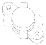
Figure 1: Pin connection
Table 1: Device summary
Order code
Marking
Package
Packing
SD2932W
SD2932(1)
M244
Tube
Notes:
(1)For
more details please refer to Section 11: "Marking, packing and shipping specifications" .
November 2016
DocID6876 Rev 10
This is information on a product in full production.
1/20
www.st.com
�Contents
SD2932
Contents
1
Electrical data .................................................................................. 3
1.1
Maximum ratings ............................................................................... 3
1.2
Thermal data ..................................................................................... 3
2
Electrical characteristics ................................................................ 4
3
Impedance data ............................................................................... 5
4
Typical performance ....................................................................... 6
4.1
Typical performance (175 MHz) ........................................................ 8
5
Test circuit (175 MHz) ...................................................................... 9
6
Test circuit photomaster ............................................................... 11
7
Typical broadband data (175-230 MHz) ........................................ 12
8
Test circuit 175 - 230 MHz ............................................................ 13
9
Typical broadband data (88 - 108 MHz) ........................................ 14
10
11
Test circuit 88-108 MHZ ................................................................ 15
Marking, packing and shipping specifications............................ 16
12
Package information ..................................................................... 17
12.1
13
2/20
M244 package information .............................................................. 17
Revision history ............................................................................ 19
DocID6876 Rev 10
�SD2932
Electrical data
1
Electrical data
1.1
Maximum ratings
TCASE = 25 °C
Table 2: Absolute maximum ratings
Symbol
1.2
Parameter
Value
Unit
V(BR)DSS
Drain source voltage
125
V
VDGR
Drain-gate voltage (RGS = 1 MΩ)
125
V
VGS
Gate-source voltage
±40
V
ID
Drain current
40
A
PDISS
Power dissipation
500
W
TJ
Max. operating junction temperature
+200
°C
TSTG
Storage temperature
-65 to +150
°C
Value
Unit
0.35
°C/W
Thermal data
Table 3: Thermal data
Symbol
RthJC
Parameter
Junction-to-case thermal resistance
DocID6876 Rev 10
3/20
�Electrical characteristics
2
SD2932
Electrical characteristics
TCASE = 25 °C
Table 4: Static
Symbol
Test conditions
Min.
Typ.
Max.
Unit
V(BR)DSS
VGS = 0 V
IDS = 100 mA
IDSS
VGS = 0 V
VDS = 50 V
50
µA
IGSS
VGS = 20 V
VDS = 0 V
250
nA
VGS(Q)
VDS = 10 V
ID = 250 mA
4
V
VDS(ON)
VGS = 10 V
ID = 10 A
3.0
V
GFS
VDS = 10 V
ID = 5 A
ΔVGS(1)
VDS = 10 V
ID = 250 mA
CISS
VGS = 0 V
VDS = 50 V
f = 1 MHz
480
pF
COSS
VGS = 0 V
VDS = 50 V
f = 1 MHz
190
pF
CRSS
VGS = 0 V
VDS = 50 V
f = 1 MHz
18
pF
125
V
1.5
5
mho
200
mV
Notes:
(1)Absolute
VGS difference between side 1 and side 2 of the device.
Table 5: Dynamic
Symbol
4/20
Test conditions
Min.
Typ.
Max.
Unit
POUT
VDD = 50 V
GPS
VDD = 50 V IDQ = 500 mA POUT = 300 W
f = 175 MHz
15
16
dB
ηD
VDD = 50 V IDQ = 500 mA POUT = 300 W
f = 175 MHz
50
60
%
Load
mismatch
VDD = 50 V IDQ = 500 mA
f = 175 MHz
All phase angles
5:1
IDQ = 500 mA
f = 175 MHz
300
W
POUT = 300 W
DocID6876 Rev 10
VSWR
�SD2932
3
Impedance data
Impedance data
Figure 2: Impedance data
Table 6: Impedance data
f
ZIN(Ω)
ZDL(Ω)
175 MHz
0.92 - j 0.14
3.17 + j 4.34
Measured gate-to-gate and drain-to-drain, respectively.
DocID6876 Rev 10
5/20
�Typical performance
4
SD2932
Typical performance
Figure 3: Maximum thermal resistance vs. case
temperature
Figure 4: Gate voltage vs. case temperature
Figure 6: Drain current vs. gate voltage
Figure 5: Capacitance vs. drain-source voltage
20
Tc=-20 °C
Tc=+25 °C
15
10
Tc=+80 °C
5
0
2
2.5
3
V
GS
6/20
DocID6876 Rev 10
3.5
4
4.5
, GATE-SOURCE VOLTAGE (V)
5
5.5
6
�SD2932
Typical performance
Figure 7: Maximum safe operating area
Figure 8: Transient thermal impedance
Figure 9: Transient thermal model
DocID6876 Rev 10
7/20
�Typical performance
4.1
8/20
SD2932
Typical performance (175 MHz)
Figure 10: Output power vs. input power
Figure 11: Output power vs. input power at different
Tc
Figure 12: Power gain vs. output power
Figure 13: Efficiency vs. output power
Figure 14: Output power vs. supply voltage
Figure 15: Output power vs. gate voltage
DocID6876 Rev 10
�SD2932
5
Test circuit (175 MHz)
Test circuit (175 MHz)
Figure 16: 175 MHz production test circuit schematic
Table 7: 175 MHz test circuit part list
Component
Description
R1, R2, R5, R6
470 Ohm 1 W, surface mount chip resistor
R3, R4
360 Ohm 0.5 W, carbon comp. axial lead resistor or equivalent
R7, R8
560 Ohm 2 W, resistor 2 turn wire air-wound axial lead resistor
R9, R10
20 kOhm 3.09 W, 10 turn wirewound precision potentiometer
C1, C4
680 pF ATC 130B surface mount ceramic chip capacitor
C2, C3, C7, C8,
C17, C19, C20,
C21
10000 pF ATC 200B surface mount ceramic chip capacitor
C5
75 pF ATC 100B surface mount ceramic chip capacitor
C6
ST40 25 pF - 115 pF miniature variable trimmer
C9, C10
47 pF ATC 100B surface mount ceramic chip capacitor
C11, C12, C13
43 pF ATC 100B surface mount ceramic chip capacitor
C14, C15, C24,
C25
1200 pF ATC 700B surface mount ceramic chip capacitor
C16, C18
470 pF ATC 700B surface mount ceramic chip capacitor
C22, C23
0.1 μF / 500 V surface mount ceramic chip capacitor
C26, C27
0.01 μF / 500 V surface mount ceramic chip capacitor
C28
10 μF / 63 aluminum electrolytic axial lead capacitor
B1
50 Ohm RG316 O.D 0.076[1.93] L = 11.80[299.72] flexible coaxial cable 4
turns through ferrite bead
B2
50 Ohm RG-142B O.D 0.165[4.19] L = 11.80[299.72] flexible coaxial cable
DocID6876 Rev 10
9/20
�Test circuit (175 MHz)
SD2932
Component
10/20
Description
T1
R.F. transformer 4:1, 25 Ohm O.D RG316-25 O.D 0.080[2.03] L =
5.90[149.86] flexible coaxial cable 2 turns through ferrite multi-aperture core
T2
R.F. transformer 1:4, 25 Ohm semi-rigid coaxial cable O.D. 0.141[3.58] L =
5.90[149.86]
L1
Inductor λ 1/4 wave 50 Ohm O.D 0.165[4.19] L = 11.80 [299.72] flexible
coaxial cable 2 turns through ferrite bead
FB1, FB5
Shield bead
FB2, FB6
Multi-aperture core
FB3
Multilayer ferrite chip bead (surface mount)
FB4
Surface mount EMI shield bead
PCB
Woven glass reinforced PTFE microwave laminate 0.06”, 1 oz EDCu, both
sides, εr = 2.55
DocID6876 Rev 10
�SD2932
6
Test circuit photomaster
Test circuit photomaster
Figure 17: 175 MHz test circuit photomaster
Figure 18: 175 MHz test fixture
DocID6876 Rev 10
11/20
�Typical broadband data (175-230 MHz)
7
SD2932
Typical broadband data (175-230 MHz)
Figure 19: Input power vs. frequency
Figure 20: Power gain vs. frequency
Figure 21: Efficiency vs. frequency
Figure 22: Return loss vs. frequency
Figure 23: 1 dB compression point vs. frequency
12/20
DocID6876 Rev 10
�SD2932
8
Test circuit 175 - 230 MHz
Test circuit 175 - 230 MHz
Figure 24: 175 - 230 MHz test circuit layout (engineering fixture)
Table 8: 175 - 230 MHz circuit layout component part list
Component
Description
PCB
1/32” woven fiberglass 0.030 Cu, sides, εr = 4.8
T1
50 Ohm flexible coax cable OD 0.06”, 3” long. ferrite core NEOSIDE
T2, T3
9:1 transformer, 16.5 Ohm flexible coax cable 0.1”, 3” long
T4, T5
4:1 transformer, 25 Ohm flexible coax cable OD 0.06”, 5” long
C1
8.2 pF ceramic cap
C2, C3
100 pF ceramic cap
C4
2 - 18 pF chip cap
C5
47 pF ceramic cap
C6, C11
47 nF ceramic cap
C7
56 pF ATC chip cap
C8, C9, C13
470 pF ATC chip cap
C10
100 nF ceramic cap
C12
2 x 330 nF / 50 V cap
C14
10 nF / 63 V electrolityc cap
R1, R3
47 Ohm resistor
R2
6.8 kOhm chip resistor
R4
4.7 kOhm multi turn trim resistor
R5
8.2 kOhm / 5 W resistor
R6
3.3 kOhm / 5 W resistor
D1
6.8 V Zener diode
L1
20 nH inductor
L2
70 nH inductor
L3
30 nH inductor
L4
10 nH inductor
L5
15 nH inductor
DocID6876 Rev 10
13/20
�Typical broadband data (88 - 108 MHz)
9
SD2932
Typical broadband data (88 - 108 MHz)
Figure 25: Input power vs. frequency (POUT=300)
Figure 26: Power gain vs. frequency (POUT=300)
Figure 27: Efficiency vs. frequency (POUT=300)
Figure 28: Return loss vs. frequency (POUT=300)
Figure 29: 2nd harmonic vs. frequency (88 - 108 MHz)
Figure 30: 3rd harmonic vs. frequency (88 - 108 MHz)
14/20
DocID6876 Rev 10
�SD2932
10
Test circuit 88-108 MHZ
Test circuit 88-108 MHZ
Figure 31: 88 - 108 MHz test circuit layout (engineering fixture)
Table 9: 88 - 108 MHz circuit layout component part list
Component
Description
PCB
1/32” woven fiberglass 0.030 Cu, sides, εr = 4.8
T1
50 Ohm flexible coax cable OD 0.06”, 3” long
T2, T3
9:1 transformer, 25 Ohm flexible coax cable 0.1”, 3.9” ferrite core
NEOSIDE
T4, T5
4:1 transformer, 25 Ohm flexible coax cable OD 0.1”, 5” long
T6
50 Ohm flexible coax cable OD 0.1”, 5” long
FB1
vk200
C1
10 pF ceramic cap
C2, C3, C4, C7, C8
1 nF chip cap
C5, C6
1 nF ATC chip cap
C9
470 pF ceramic cap
C10
100 nF chip cap
C11
100 mF / 63 V electrolytic cap
R1
56 Ohm resistor
R2, R4
10 Ohm chip resistor
R3
10 kOhm resistor
R5
5.6 Ohm resistor
R6
10 kOhm, 10 turn trim resistor
R7
3.3 kOhm / 5 W resistor
R8
15 Ohm / 5 W resistor
D1
6.8 V Zener diode
L1
10 nH inductor
L2
40 nH inductor
L3
70 nH inductor
DocID6876 Rev 10
15/20
�Marking, packing and shipping specifications
11
SD2932
Marking, packing and shipping specifications
Table 10: Packing and shipping specifications
Order code
Packing
Pieces
per tray
Dry pack
humidity
VGS and GFS
code
Lot code
SD2932W
Tube
15
< 10%
Not mixed
Not mixed
Figure 32: SD2932 marking layout
Table 11: Marking specifications
Symbol
W
Wafer process code
CZ
Assembly plant
xxx
Last 3 digits of diffusion lot
VY
Diffusion plant
MAR
CZ
16/20
Description
Country of origin
Test and finishing plant
y
Assembly year
yy
Assembly week
DocID6876 Rev 10
�SD2932
12
Package information
Package information
In order to meet environmental requirements, ST offers these devices in different grades of
ECOPACK® packages, depending on their level of environmental compliance. ECOPACK ®
specifications, grade definitions and product status are available at: www.st.com.
ECOPACK® is an ST trademark.
12.1
M244 package information
Figure 33: M244 (0.400 x .860 4L BAL N/HERM W/FLG) package outline
DocID6876 Rev 10
17/20
�Package information
SD2932
Table 12: M244 (0.400 x .860 4L BAL N/HERM W/FLG) package mechanical data
mm
Dim.
Min.
A
5.59
B
Max.
5.84
5.08
C
3.02
3.28
D
E
9.65
19.81
9.91
20.82
F
10.92
11.18
27.94
G
18/20
Typ.
H
33.91
34.16
I
0.10
0.15
J
1.78
K
1.52
2.59
L
4.83
5.84
M
10.03
10.34
N
21.59
22.10
DocID6876 Rev 10
2.84
�SD2932
13
Revision history
Revision history
Table 13: Document revision history
Date
Revision
Changes
15-Jul-2004
5
24-Jan-2006
6
Updated Table 4: Static (per section).
23-Nov-2009
7
Inserted ΔVGS in Table 4: Static (per section).
31-Mar-2010
8
Added Figure 7, Figure 8 and Figure 9.
11-Jan-2012
9
Inserted Chapter 12: Marking, packing and shipping
specifications.
Minor text changes.
24-Nov-2016
10
Updated Section 1.1: "Maximum ratings".
DocID6876 Rev 10
19/20
�SD2932
IMPORTANT NOTICE – PLEASE READ CAREFULLY
STMicroelectronics NV and its subsidiaries (“ST”) reserve the right to make changes, corrections, enhancements, modifications, and
improvements to ST products and/or to this document at any time without notice. Purchasers should obtain the latest relevant information on ST
products before placing orders. ST products are sold pursuant to ST’s terms and conditions of sale in place at the time of order
acknowledgement.
Purchasers are solely responsible for the choice, selection, and use of ST products and ST assumes no liability for application assistance or the
design of Purchasers’ products.
No license, express or implied, to any intellectual property right is granted by ST herein.
Resale of ST products with provisions different from the information set forth herein shall void any warranty granted by ST for such product.
ST and the ST logo are trademarks of ST. All other product or service names are the property of their respective owners.
Information in this document supersedes and replaces information previously supplied in any prior versions of this document.
© 2016 STMicroelectronics – All rights reserved
20/20
DocID6876 Rev 10
�