®
SM6HTxxA
HIGH TEMPERATURE TRANSILTM FOR AUTOMOTIVE APPLICATIONS
FEATURES HIGH PERFORMANCE TRANSIL DESIGNED TO FIT HIGH TEMPERATURE ENVIRONMENT LIKE AUTOMOTIVE APPLICATIONS... HIGH RELIABILITY PLANAR TECHNOLOGY HIGH PERFORMANCE IN VOLTAGE REGULATION MODE VERY LOW LEAKAGE CURRENT (IR max = 5µA @ Tamb = 150°C) PEAK PULSE POWER : 600 W (10/1000µs) FAST RESPONSE TIME UNIDIRECTIONAL TYPE LOW CLAMPING FACTOR DESCRIPTION This high performance Transil series has been designed to fit high temperature environment such as automotive applications, using surface mount technology. These devices are using high reliability planar technology resulting in high performances in voltage regulation mode and low leakage current at high temperature. ABSOLUTE MAXIMUM RATINGS (Tamb = 25°C) Symbol PPP P IFSM Tstg, TJ TL Parameter Peak pulse power dissipation (see note 1) Power dissipation on infinite heatsink Non repetitive surge peak forward current for unidirectional types Tj initial = Tamb Tamb = 50°C tp = 10ms Tj initial = Tamb Value 600 5 75 - 65 to 175 260 Unit W W A °C °C
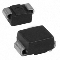
SMB (JEDEC D0-214AA)
Storage and operating junction temperature range Maximum lead temperature for soldering during 10 s.
Note 1 : For a surge greater than the maximum values, the diode will fail in short-circuit.
THERMAL RESISTANCES Symbol Rth (j-l) Rth (j-a) Junction to leads Junction to ambient on printed circuit. On recommended pad layout Parameter Value 20 100 Unit °C/W °C/W
April 1999 Ed: 4A
1/5
�SM6HTxxA
ELECTRICAL CHARACTERISTICS (Tamb = 25°C unless otherwise specified) Symbol VRM VBR VCL IRM IPP VF Parameter
IF I
Stand-off voltage Breakdown voltage Clamping voltage Leakage current @ VRM Peak pulse current Forward voltage drop VF < 3.5V @ IF = 50A
(pulse test: tp ≤ 500µs)
I PP VCL VBR V RM VF I RM V
Types
Marking
IRM
@
VRM min V 22.8 25.7 28.5 34.2 37.1 40.9
VBR note2 nom V 24 27 30 36 39 43
@
IR
VCL @ IPP 10/1000µs max V A 33.2 18.0 37.5 41.5 49.9 53.9 59.3 16.0 14.5 12.0 11.1 10.1
αT max note 3 10-4/°C 9.4 9.6 9.7 9.9 10.0 10.1
SM6HT24A SM6HT27A SM6HT30A SM6HT36A SM6HT39A SM6HT43A
EMB EPB ERB EVB EXB EYB
Tamb=25°C Tamb=150°C max max µA µA 2 5 2 2 2 2 2 5 5 5 5 5
V 20.5 23.1 25.6 30.8 33.3 36.8
max V 25.2 28.4 31.5 37.8 41.0 45.2
mA 1 1 1 1 1 1
Note 2 : Pulse test : tp < 50 ms Note 3 : ∆VBR = αT x (Tamb - 25) x VBR (25°C)
2/5
�SM6HTxxA
Fig. 1-1: Peak power dissipation versus initial junction temperature. Fig. 1-2: Continous power dissipation versus ambient temperature.
Ppp[Tj initial] / Ppp[Tj initial=25°C] 1.1 1.0 0.9 0.8 0.7 0.6 0.5 0.4 0.3 0.2 0.1 0.0
6 5 4 3 2 1
P(W)
Rth(j-a)=Rth(j-l)
Rth(j-a)=100°C/W
Tj initial(°C) 0 25 50 75 100 125 150 175 200
0
Tamb(°C) 0 25 50 75 100 125 150 175
Fig. 2: Peak pulse power versus exponential pulse duration (Tj initial=25°C).
Fig. 3: Clamping voltage versus peak pulse current (Tj initial=25°C).
10.0
Ppp(kW)
Ipp(A) 1E+2
SM6HT27A SM6HT24A SM6HT30A SM6HT36A SM6HT39A
tp=20µs
1E+1
SM6HT43A
1.0
1E+0
tp=1ms
tp(ms) 0.1 0.01 0.10 1.00 10.00
1E-1 10
Vcl(V)
100
Fig. 4: Junction capacitance versus reverse applied voltage (typical values).
Fig. 5: Peak forward voltage drop versus peak forward current (typical values).
C(pF) 1000
F=1MHz
100.0
IFM(A)
500
SM6HT24A
10.0
Tj=175°C
Tj=25°C
SM6HT27A
200 VR(V) 1 10
SM6HT30A SM6HT36A SM6HT39A SM6HT43A
1.0
100
100
200
0.1 0.5
VFM(V) 1.0 1.5 2.0 2.5 3.0 3.5
3/5
�SM6HTxxA
Fig. 6: Variation of thermal impedance junction to ambient versus pulse duration (Printed circuit board FR4 with recommended pad layout).
Zth(j-a)(°C/W)
Fig. 7: Thermal resistance junction to ambient versus copper surface under each lead (printed circuit board FR4, e(Cu)=35µm).
100 90 Rth(j-a) (°C/W)
1E+2
1E+1
80 70
1E+0 tp(s) 1E-1 1E-3 1E-2 1E-1 1E+0 1E+1 1E+2 5E+2
60 50 S(cm²) 40 0 1 2 3 4 5
Fig .8: Variation of leakage current versus junction temperature (typical values).
1E+4 1E+3 1E+2 1E+1 1E+0 1E-1 1E-2 1E-3
IR(µA)
1E-4 25
Tj(°C) 50 75 100 125 150 175
4/5
�SM6HTxxA
MARKING : Logo, Date Code, Type Code, Cathode Band. PACKAGE MECHANICAL DATA SMB (Plastic) DIMENSIONS
E1
REF.
D
Millimeters Min. Max. 2.45 0.20 2.20 0.41 5.60 4.60 3.95 1.60 1.90 0.05 1.95 0.15 5.10 4.05 3.30 0.75
Inches Min. 0.075 0.002 0.077 0.006 0.201 0.159 0.130 0.030 Max. 0.096 0.008 0.087 0.016 0.220 0.181 0.156 0.063
A1 A2 b
E
c
A1
E E1
b
C L
A2
D L
Weight = 0.107 g FOOTPRINT DIMENSIONS (Millimeter) SMB Plastic.
2.3
1.52
2.75
1.52
Packaging : standard packaging is tape and reel.
Information furnished is believed to be accurate and reliable. However, STMicroelectronics assumes no responsibility for the consequences of use of such information nor for any infringement of patents or other rights of third parties which may result from its use. No license is granted by implication or otherwise under any patent or patent rights of STMicroelectronics. Specifications mentioned in this publication are subject to change without notice. This publication supersedes and replaces all information previously supplied. STMicroelectronics products are not authorized for use as critical components in life support devices or systems without express written approval of STMicroelectronics.
The ST logo is a registered trademark of STMicroelectronics © 1999 STMicroelectronics - Printed in Italy - All rights reserved. STMicroelectronics GROUP OF COMPANIES Australia - Brazil - Canada - China - France - Germany - Italy - Japan - Korea - Malaysia - Malta - Mexico - Morocco The Netherlands - Singapore - Spain - Sweden - Switzerland - Taiwan - Thailand - United Kingdom - U.S.A. http://www.st.com 5/5
�
很抱歉,暂时无法提供与“SM6HT36A”相匹配的价格&库存,您可以联系我们找货
免费人工找货- 国内价格 香港价格
- 5000+2.393055000+0.31000