SMA6JxxA, SMA6JxxCA
Datasheet
600 W TVS in SMA
Features
•
•
Peak pulse power:
–
600 W (10/1000 μs)
–
4 kW (8/20 μs)
Stand-off voltage range from 5 V to 85 V
Unidirectional and bidirectional types
Low leakage current:
–
0.2 µA at 25 °C
–
1 μA at 85 °C
Operating Tj max: 175 °C
•
•
JEDEC registered package outline
Resin meets UL94, V0
•
•
•
Product status link
SMA6J5.0A, SMA6J5.0CA,
SMA6J6.0A, SMA6J6.0CA,
SMA6J6.5A, SMA6J6.5CA,
SMA6J8.5A, SMA6J8.5CA,
SMA6J10A, SMA6J10CA,
SMA6J12A, SMA6J12CA,
SMA6J13A, SMA6J13CA,
SMA6J15A, SMA6J15CA,
SMA6J18A, SMA6J18CA,
SMA6J20A, SMA6J20CA,
SMA6J24A, SMA6J24CA,
SMA6J26A, SMA6J26CA,
SMA6J28A, SMA6J28CA,
Complies with the following standards
•
•
•
•
•
•
•
•
UL94, V0
J-STD-020 MSL level 1
J-STD-002, JESD 22-B102 E3 and MIL-STD-750, method 2026 solderable
matte tin plated leads
JESD-201 class 2 whisker test
IPC7531 footprint
JEDEC registered package outline
IEC 61000-4-4 level 4:
–
4 kV
IEC 61000-4-2, C = 150 pF - R = 330 Ω exceeds level 4:
–
30 kV (air discharge)
–
30 kV (contact discharge)
SMA6J33A, SMA6J33CA,
SMA6J40A, SMA6J40CA,
SMA6J48A, SMA6J48CA,
SMA6J58A, SMA6J58CA,
SMA6J70A, SMA6J70CA,
SMA6J85A, SMA6J85CA.
Description
The SMA6J series is designed to protect sensitive equipment against electrostatic
discharges according to IEC 61000-4-2 and MIL STD 883, method 3015, and
electrical overstress according to IEC 61000-4-4 and 5. This device is more generally
used against surges below 600 W (10/1000 μs).
The Planar technology makes it compatible with high-end circuits where low leakage
current and high junction temperature are required to provide long term reliability and
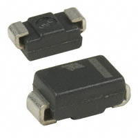
stability. SMA6J devices are packaged in SMA (SMA footprint in accordance with IPC
7531 standard).
DS5142 - Rev 10 - May 2022
For further information contact your local STMicroelectronics sales office.
www.st.com
�SMA6JxxA, SMA6JxxCA
Characteristics
1
Characteristics
Table 1. Absolute maximum ratings (Tamb = 25 °C)
Symbol
Parameter
Value
Unit
Contact discharge
30
kV
Air discharge
30
Tj initial = Tamb
600
W
IEC 61000-4-2 (C = 150 pF, R = 330 Ω)
VPP
Peak pulse voltage
PPP
Peak pulse power dissipation
Tstg
Storage temperature range
-65 to +175
°C
Tj
Operating junction temperature range
-55 to +175
°C
TL
Maximum lead temperature for soldering during 10 s
260
°C
Figure 1. Electrical characteristics - parameter definitions
Figure 2. Pulse definition for electrical characteristics
DS5142 - Rev 10
page 2/12
�SMA6JxxA, SMA6JxxCA
Characteristics
Table 2. Electrical characteristics - parameter values (Tamb = 25 °C, unless otherwise specified)
Type
25 °C 85 °C
µA
10 / 1000 µs
VBR at IBR (1)
IRM max at VRM
VCL(2)(3)
Min. Typ. Max.
V
V
IPP(4)
Max.
8 / 20µs
RD
VCL(2)(3)
Max.
Max.
IPP(4)
RD
αT
Max.
Max.
mA
V
A
Ω
V
A
Ω
10-4/°C
SMA6J5.0A/CA
20
50
5.0 6.40 6.74
7.07
10
9.1
68
0.029
14.4
275
0.027
5.7
SMA6J6.0A/CA
20
50
6.0 6.70 7.05
7.41
10
9.5
61
0.034
14.8
270
0.027
5.9
SMA6J6.5A/CA
20
50
6.5 7.20 7.58
7.96
10
10.2
56
0.040
15.2
266
0.027
6.1
SMA6J8.5A/CA
20
50
8.5
9.4
9.9
10.4
1
13.3
41.7
0.070
19.5
205
0.044
7.3
SMA6J10A/CA
0.2
1
10
11.1
11.7
12.3
1
15.7
37
0.093
21.7
184
0.051
7.8
SMA6J12A/CA
0.2
1
12
13.3 14.0
14.7
1
18.8
31
0.133
25.3
157
0.068
8.3
SMA6J13A/CA
0.2
1
13
14.4 15.2
15.9
1
20.4
29
0.154
27.2
147
0.076
8.4
SMA6J15A/CA
0.2
1
15
16.7 17.6
18.5
1
23.6
25.1
0.206
32.5
123
0.114
8.8
SMA6J18A/CA
0.2
1
18
20.0 21.1
22.1
1
28.3
21.5
0.288
39.3
102
0.168
9.2
SMA6J20A/CA
0.2
1
20
22.2 23.4
24.5
1
31.4
19.4
0.354
42.8
93
0.196
9.4
SMA6J24A/CA
0.2
1
24
26.7 28.1
29.5
1
37.8
16
0.516
50
80
0.256
9.6
SMA6J26A/CA
0.2
1
26
28.9 30.4
31.9
1
40.9
14.9
0.600
53.5
75
0.288
9.7
SMA6J28A/CA
0.2
1
28
31.1 32.7
34.4
1
44.0
13.8
0.697
59
68
0.363
9.8
SMA6J33A/CA
0.2
1
33
36.7 38.6
40.6
1
51.9
11.8
0.963
69
57
0.512
10.0
SMA6J40A/CA
0.2
1
40
44.4 46.7
49.1
1
62.8
9.7
1.42
84
48
0.728
10.1
SMA6J48A/CA
0.2
1
48
53.3 56.1
58.9
1
75.4
8.1
2.04
100
40
1.03
10.3
SMA6J58A/CA
0.2
1
58
64.4 67.8
71.2
1
91.1
6.7
2.97
121
33
1.51
10.4
SMA6J70A/CA
0.2
1
70
77.8 81.9
86.0
1
110
5.5
4.38
146
27
2.22
10.5
SMA6J85A/CA
0.2
1
85
104
1
134
4.6
6.45
178
22.5
3.29
10.6
94
99
1. To calculate VBR versus Tj : VBR at Tj = VBR at 25 °C x (1 + αT x (Tj - 25))
2. To calculate VCL versus Tj : VCL at Tj = VCL at 25 °C x (1 + αT x (Tj - 25))
3. To calculate VCL max versus IPPappli: VCLmax = VBR max + RD x IPPappli
4. Surge capability given for both directions for unidirectional and bidirectional devices
DS5142 - Rev 10
page 3/12
�SMA6JxxA, SMA6JxxCA
Characteristics (curves)
1.1
Characteristics (curves)
Figure 3. Maximum peak power dissipation versus initial
junction temperature
Figure 4. Maximum peak pulse power versus exponential
pulse duration
PPP (kW)
PPP (W)
800
100
Tj initial = 25 °C
10/1000 µs
700
600
10
500
400
300
1
200
100
Tj (°C)
0
0
25
50
75
100
125
150
175
200
Figure 5. Maximum peak pulse current versus clamping
voltage
IPP (A)
1000
tp (ms)
0,1
0,001
0,01
0,1
1
10
Figure 6. Dynamic resistance versus pulse duration
RD (Ω)
100
8/20 µs
/CA
5A
J8
A6
10/1000 µs
SM
10
/CA
8A
100
J4
A6
SM
SM
1
10
A
A/C
J26
A6
/CA
15A
A6J
SM
0,1
SMA6J85A/CA
SMA6J48A/CA
SMA6J26A/CA
SMA6J15A/CA
SMA6J5.0A/CA
1
SMA
VCL (V)
0,1
1
10
100
1000
Figure 7. Junction capacitance versus reverse applied
voltage (unidirectional type)
A/CA
6J5.0
tp (ms)
0,01
0,01
0,1
1
10
Figure 8. Junction capacitance versus applied voltage
(bidirectional type)
C (pF)
C (pF)
10000
10000
f=1MHz
Vosc=30mVRMS
Tj=25°C
f=1MHz
Vosc=30mVRMS
Tj=25°C
SMA6J5.0A
1000
SMA6J5.0CA
1000
SMA6J15A
SMA6J15CA
SMA6J26A
100
100
SMA6J26CA
SMA6J48A
SMA6J48CA
SMA6J85A
VR (V)
10
1
DS5142 - Rev 10
10
100
1000
SMA6J85CA
10
1
10
100
VR (V)
1000
page 4/12
�SMA6JxxA, SMA6JxxCA
Characteristics (curves)
Figure 9. Leakage current versus junction temperature
Figure 10. Peak forward voltage drop versus peak forward
current
IR (nA)
10000
IF (A)
10
VR=VRM
single pulse
1000
VRM < 11.7V
Tj=125 °C
100
1
10
VRM ≥ 11.7V
Tj=25 °C
1
Tj (°C)
0
25
50
75
100
125
150
175
VF (V)
0,1
0,4
Figure 11. Thermal impedance junction to ambient versus
pulse duration
1000
Zth(j-a) (°C/W)
0,6
0,7
0,8
0,9
1
1,1
1,2
1,3
1,4
Figure 12. Thermal resistance junction to ambient versus
copper area under each lead
Rth(j-a) (°C/W)
160
Single pulse on recommended footprint.
Epoxy printed circuit board FR4, 70 µm Cu thickness
0,5
Single pulse on recommended footprint.
Epoxy printed circuit board FR4, 70 µm Cu thickness
140
120
100
100
80
60
10
40
20
1
0.01
DS5142 - Rev 10
t p (s)
0.1
1
10
100
SCu (cm²)
0
1000
0
0.5
1
1.5
2
2.5
3
3.5
4
4.5
5
page 5/12
�SMA6JxxA, SMA6JxxCA
Package information
2
Package information
In order to meet environmental requirements, ST offers these devices in different grades of ECOPACK packages,
depending on their level of environmental compliance. ECOPACK specifications, grade definitions and product
status are available at: www.st.com. ECOPACK is an ST trademark.
2.1
SMA package information
Figure 13. SMA package outline
E1
D
E
A1
C
A2
L
b
Table 3. SMA package mechanical data
Dimensions
Millimeters
Ref.
Inches
Min.
Max.
Min.
Max.
A1
1.90
2.45
0.074
0.097
A2
0.05
0.20
0.001
0.008
b
1.25
1.65
0.049
0.065
c
0.15
0.40
0.005
0.016
D
2.25
2.90
0.088
0.115
E
4.80
5.35
0.188
0.211
E1
3.95
4.60
0.155
0.182
L
0.75
1.50
0.029
0.060
DS5142 - Rev 10
page 6/12
�SMA6JxxA, SMA6JxxCA
SMA package information
Figure 14. SMA recommended footprint in mm (inches)
1.40
(0.055)
2.63
(0.104)
Figure 15. SMA marking
1.40
(0.055)
1.64
(0.065)
5.43
(0.214)
Figure 16. Package orientation in reel
Figure 17. Tape and reel orientation
Figure 18. 13'' reel dimension values
Figure 19. Inner box dimension values
DS5142 - Rev 10
page 7/12
�SMA6JxxA, SMA6JxxCA
SMA package information
Figure 20. Tape outline
Table 4. Tape dimension values
Dimensions
Millimeters
Ref.
DS5142 - Rev 10
Min.
Typ.
Max.
D0
1.40
1.50
1.60
D1
1.50
F
5.40
5.50
5.60
K0
2.26
2.36
2.46
P0
3.90
4.00
4.10
P1
3.90
4.00
4.10
P2
1.95
2.00
2.05
W
11.70
12.00
12.30
page 8/12
�SMA6JxxA, SMA6JxxCA
Reflow profile
2.2
Reflow profile
Figure 21. ST ECOPACK recommended soldering reflow profile for PCB mounting
250
240-245 °C
Temperature (°C)
-2 °C/s
2 - 3 °C/s
60 sec
(90 max)
200
-3 °C/s
150
-6 °C/s
100
0.9 °C/s
50
Time (s)
0
Note:
DS5142 - Rev 10
30
60
90
120
150
180
210
240
270
300
Minimize air convection currents in the reflow oven to avoid component movement. Maximum soldering profile
corresponds to the latest IPC/JEDEC J-STD-020.
page 9/12
�SMA6JxxA, SMA6JxxCA
Ordering information
3
Ordering information
Table 5. Ordering information
Order code
Marking
Package
Weight
Base qty.
Delivery mode
SMA6JxxA/CA(1)
See Table 6. Marking.
SMA
72 mg
5000
Tape and reel
1. Where xx is VRM and A or CA indicates unidirectional or bidirectional version.
Table 6. Marking
DS5142 - Rev 10
Type
Marking
Type
Marking
SMA6J5.0A-TR
6UA
SMA6J5.0CA-TR
6BA
SMA6J6.0A-TR
6UB
SMA6J6.0CA-TR
6BB
SMA6J6.5A-TR
6UC
SMA6J6.5CA-TR
6BC
SMA6J8.5A-TR
6UD
SMA6J8.5CA-TR
6BD
SMA6J10A-TR
6UE
SMA6J10CA-TR
6BE
SMA6J12A-TR
6UF
SMA6J12CA-TR
6BF
SMA6J13A-TR
6UG
SMA6J13CA-TR
6BG
SMA6J15A-TR
6UH
SMA6J15CA-TR
6BH
SMA6J18A-TR
6UJ
SMA6J18CA-TR
6BJ
SMA6J20A-TR
6UK
SMA6J20CA-TR
6BK
SMA6J24A-TR
6UM
SMA6J24CA-TR
6BM
SMA6J26A-TR
6UN
SMA6J26CA-TR
6BN
SMA6J28A-TR
6UO
SMA6J28CA-TR
6BO
SMA6J33A-TR
6UQ
SMA6J33CA-TR
6BQ
SMA6J40A-TR
6UR
SMA6J40CA-TR
6BR
SMA6J48A-TR
6US
SMA6J48CA-TR
6BS
SMA6J58A-TR
6UT
SMA6J58CA-TR
6BT
SMA6J70A-TR
6UU
SMA6J70CA-TR
6BU
SMA6J85A-TR
6UV
SMA6J85CA-TR
6BV
page 10/12
�SMA6JxxA, SMA6JxxCA
Revision history
Table 7. Document revision history
DS5142 - Rev 10
Date
Revision
Changes
21-Feb-2007
1
First issue.
7-Nov-2007
2
Updated Description. Improved readability of Ordering information scheme.
Reformatted to current standards.
04-Aug-2014
3
Updated weight in Table 7.
28-Oct-2015
4
Updated Table 4 and Figure 3.
04-Jul-2017
5
Updated Table 4.
22-Jan-2018
6
Updated Table3.
30-Aug-2018
7
Updated Table 6. Marking.
30-Mar-2022
8
Update after termination of VRM > 90 V. Minor text changes.
04-May-2022
9
Updated Description.
31-May-2022
10
Minor text changes.
page 11/12
�SMA6JxxA, SMA6JxxCA
IMPORTANT NOTICE – READ CAREFULLY
STMicroelectronics NV and its subsidiaries (“ST”) reserve the right to make changes, corrections, enhancements, modifications, and improvements to ST
products and/or to this document at any time without notice. Purchasers should obtain the latest relevant information on ST products before placing orders. ST
products are sold pursuant to ST’s terms and conditions of sale in place at the time of order acknowledgment.
Purchasers are solely responsible for the choice, selection, and use of ST products and ST assumes no liability for application assistance or the design of
purchasers’ products.
No license, express or implied, to any intellectual property right is granted by ST herein.
Resale of ST products with provisions different from the information set forth herein shall void any warranty granted by ST for such product.
ST and the ST logo are trademarks of ST. For additional information about ST trademarks, refer to www.st.com/trademarks. All other product or service names
are the property of their respective owners.
Information in this document supersedes and replaces information previously supplied in any prior versions of this document.
© 2022 STMicroelectronics – All rights reserved
DS5142 - Rev 10
page 12/12
�