0
登录后你可以
  • 下载海量资料
  • 学习在线课程
  • 观看技术视频
  • 写文章/发帖/加入社区
会员中心
创作中心
发布
  • 发文章

  • 发资料

  • 发帖

  • 提问

  • 发视频

创作活动
SMA6J85A-TR

SMA6J85A-TR

  • 厂商:

    STMICROELECTRONICS(意法半导体)

  • 封装:

    SMA(DO-214AC)

  • 描述:

  • 详情介绍
  • 数据手册
  • 价格&库存
SMA6J85A-TR 数据手册
SMA6J High junction temperature Transil™ Features ■ Peak pulse power: – 600 W (10/1000 µs) – 4 kW (8/20 µs) Stand off voltage range: from 5 V to 188 V Unidirectional and bidirectional types Low clamping voltage versus standard series Low leakage current: – 0.2 µA at 25° C – 1 µA at 85° C Operating Tj max: 175° C JEDEC registered package outline ■ ■ ■ ■ A K Unidirectional Bidirectional ■ ■ SMA (JEDEC DO-214AC) Description The SMA6J Transil series has been designed to protect sensitive equipment against electro-static discharges according to IEC 61000-4-2, MIL STD 883 Method 3015, and electrical over stress such as IEC 61000-4-4 & 5. They are also in accordance with ISO TR 7637-2, SAE J 113 and DIN 40839 for automotive applications and more generally for surges below 600 W 10/1000 µs This Planar technology makes it compatible with high-end equipment like automotive, medical equipment or SMPS where low leakage current and high junction temperature are required to provide reliability and stability over time. Their low clamping voltages provides a better safety margin to protect sensitive circuits with extended life time expectancy. Packaged in SMA, this minimizes PCB consumption (SMA footprint in accordance with IPC 7531 standard). Order code Part number SMA6JxxA-TR SMA6JxxCA-TR Marking See Table 6. See Table 6. Complies with the following standards: IEC 61000-4-2 level 4: 15 kV(air discharge) 8 kV(contact discharge) MIL STD 893G-Method 3015-7: class3B 25 kV HBM (Human Body Model) TM: TRANSIL is a trademark of STMicroelectronics February 2007 Rev 1 1/10 www.st.com 10 Characteristics SMA6J 1 Table 1. Symbol PPP P IFSM Tstg Tj TL Characteristics Absolute ratings (Tamb = 25° C) Parameter Peak pulse power dissipation (1) Power dissipation on infinite heatsink Non repetitive surge peak forward current for unidirectional types Storage temperature range Operating junction temperature range Maximum lead temperature for soldering during 10 s Tj initial = Tamb Tamb = 55° C tp = 10 ms Tj initial = Tamb Value 600 4 60 -65 to +175 -55 to +175 260 Unit W W A °C °C °C 1. For a surge greater than the maximum values, the diode will fail in short-circuit. Table 2. Symbol Rth (j-l) Rth (j-a) Thermal resistances Parameter Junction to leads Junction to ambient on printed circuit on recommended pad layout Value 30 120 Unit ° C/W ° C/W Table 3. Symbol VRM VBR VCL IRM IPP αT VF RD Electrical characteristics - definitions (Tamb = 25° C) Parameter Stand-off voltage Breakdown voltage Clamping voltage Leakage current @ VRM Peak pulse current Voltage temperature coefficient Forward voltage drop Dynamic resistance IPP Unidirectional I IF I IPP VCL VBR VRM IRM IR VF V VCLVBR VRM IR IRM IRM IR V VRMVBR VCL IPP Bidirectional 2/10 SMA6J Table 4. Electrical characteristics - values (Tamb = 25° C) IRM max@VRM Type 25° C 85° C µA SMA6J5.0A/CA SMA6J6.0A/CA SMA6J6.5A/CA SMA6J8.5A/CA SMA6J10A/CA SMA6J12A/CA SMA6J13A/CA SMA6J15A/CA SMA6J18A/CA SMA6J20A/CA SMA6J24A/CA SMA6J26A/CA SMA6J28A/CA SMA6J33A/CA SMA6J40A/CA SMA6J48A/CA SMA6J58A/CA SMA6J70A/CA SMA6J85A/CA SMA6J100A/CA SMA6J130A/CA SMA6J154A/CA SMA6J170A/CA SMA6J188A/CA 10 10 10 10 0.2 0.2 0.2 0.2 0.2 0.2 0.2 0.2 0.2 0.2 0.2 0.2 0.2 0.2 0.2 0.2 0.2 0.2 0.2 0.2 50 50 50 50 1 1 1 1 1 1 1 1 1 1 1 1 1 1 1 1 1 1 1 1 V min VBR @IR(1) typ max V mA Characteristics VCL @IPP RD(2) VCL @IPP RD(2) 10/1000 µs 10/1000 µs 8/20 µs 8/20 µs max V 9.1 9.5 A 68 61 56 Ω 0.029 0.034 0.040 0.070 0.093 0.133 0.154 0.206 0.288 0.354 0.516 0.600 0.697 0.963 1.42 2.04 2.97 4.38 6.45 9.03 14.9 22.1 30.0 48.5 max V A Ω 0.021 0.022 0.024 0.041 0.040 0.056 0.054 0.075 0.108 0.132 0.184 0.213 0.253 0.356 0.511 0.736 0.863 1.27 1.85 2.58 4.24 6.00 7.39 8.97 αT(3) max 10-4/°C 5.7 5.9 6.1 7.3 7.8 8.3 8.4 8.8 9.2 9.4 9.6 9.7 9.8 10.0 10.1 10.3 10.4 10.5 10.6 10.7 10.8 10.8 10.8 10.8 5.0 6.40 6.74 7.07 10 6.0 6.70 7.05 7.41 10 13.4 298 13.7 290 14.5 276 18.7 205 19.6 184 23.5 157 23.9 147 27.7 123 33.2 102 36.8 93 44.3 80 47.9 75 51.6 68 60.8 57 73.6 48 88.4 40 100 120 33 27 6.5 7.20 7.58 7.96 10 10.2 8.5 9.4 9.9 10.4 1 1 1 1 1 1 1 1 1 1 1 1 1 1 1 1 1 1 1 1 1 13.3 41.7 15.7 18.8 20.4 37 31 29 10 11.1 11.7 12.3 12 13.3 14.0 14.7 13 14.4 15.2 15.9 15 16.7 17.6 18.5 18 20.0 21.1 22.1 20 22.2 23.4 24.5 24 26.7 28.1 29.5 26 28.9 30.4 31.9 28 31.1 32.7 34.4 33 36.7 38.6 40.6 40 44.4 46.7 49.1 48 53.3 56.1 58.9 58 64.4 67.8 71.2 70 77.8 81.9 86.0 85 94 99 117 152 180 199 220 104 123 159 189 209 231 23.6 25.1 28.3 21.5 31.4 19.4 37.8 16 40.9 14.9 44.0 13.8 51.9 11.8 62.8 75.4 91.1 110 134 157 204 242 275 328 9.7 8.1 6.7 5.5 4.6 3.8 3 2.4 2.2 2 146 22.5 172 223 19 15 100 111 130 144 154 171 170 189 188 209 265 12.6 292 11.3 323 10.3 1. Pulse test: tp 11.7V SCU(cm2) 1.E+00 25 50 75 Tj(°C) 100 125 150 175 5/10 Order information scheme SMA6J 2 Order information scheme SM Surface Mount Package A = SMA package Surge rating 6J = 600 W Stand off voltage example - 85 = 85 V Type A = Unidirectional CA = Bidirectional Packaging TR = Tape and reel A 6J xx CA - TR 6/10 SMA6J Package information 3 Package information ● ● ● ● ● Case: JEDEC DO-214AC molded plastic over Planar junction Terminals: Solder plated, solderable per MIL-STD-750, Method 2026 Polarity: For unidirectional types the band indicates cathode. Flammability: Epoxy is rated UL94V-0 RoHS package SMA Dimensions Dimensions Ref. E1 Table 5. Millimeters Min. Max. 2.03 0.20 1.65 0.40 2.90 5.35 4.60 1.50 Inches Min. 0.075 0.002 0.049 0.006 0.089 0.189 0.156 0.030 Max. 0.08 0.008 0.065 0.016 0.114 0.211 0.181 0.059 D A1 A2 b 1.90 0.05 1.25 0.15 2.25 4.80 3.95 0.75 E c A1 D E b C L A2 E1 L Figure 10. SMA footprint dimensions 1.40 (0.055) 2.63 (0.104) 1.40 (0.055) Figure 11. Marking information Cathode bar (unidirectional devices only ) (0.065) 1.64 e3 5.43 (0.214) xxx z y ww e3: ECOPACK ( Leadfree) XXX: Marking Z: Manufacturing location Y: Year WW: week milimeters (inches) 7/10 Package information Table 6. Marking Type SMA6J5.0A-TR SMA6J6.0A-TR SMA6J6.5A-TR SMA6J8.5A-TR SMA6J10A-TR SMA6J12A-TR SMA6J13A-TR SMA6J15A-TR SMA6J18A-TR SMA6J20A-TR SMA6J24A-TR SMA6J26A-TR SMA6J28A-TR SMA6J33A-TR SMA6J40A-TR SMA6J48A-TR SMA6J58A-TR SMA6J70A-TR SMA6J85A-TR SMA6J100A-TR SMA6J130A-TR SMA6J154A-TR SMA6J170A-TR SMA6J188A-TR Marking 6UA 6UB 6UC 6UD 6UE 6UF 6UG 6UH 6UJ 6UK 6UM 6UN 6UO 6UQ 6UR 6US 6UT 6UU 6UV 6UW 6UX 6UY 6UZ 6UAA Type SMA6J5.0CA-TR SMA6J6.0CA-TR SMA6J6.5CA-TR SMA6J8.5CA-TR SMA6J10CA-TR SMA6J12CA-TR SMA6J13CA-TR SMA6J15CA-TR SMA6J18CA-TR SMA6J20CA-TR SMA6J24CA-TR SMA6J26CA-TR SMA6J28CA-TR SMA6J33CA-TR SMA6J40CA-TR SMA6J48CA-TR SMA6J58CA-TR SMA6J70CA-TR SMA6J85CA-TR SMA6J100CA-TR SMA6J130CA-TR SMA6J154CA-TR SMA6J170CA-TR SMA6J188CA-TR Marking 6BA 6BB 6BC 6BD 6BE 6BF 6BG 6BH 6BJ 6BK 6BM 6BN 6BO 6BQ 6BR 6BS 6BT 6BU 6BV 6BW 6BX 6BY 6BZ 6BAA SMA6J In order to meet environmental requirements, ST offers these devices in ECOPACK® packages. These packages have a Lead-free second level interconnect . The category of second level interconnect is marked on the package and on the inner box label, in compliance with JEDEC Standard JESD97. The maximum ratings related to soldering conditions are also marked on the inner box label. ECOPACK is an ST trademark. ECOPACK specifications are available at: www.st.com. 8/10 SMA6J Ordering information 4 Ordering information Delivery mode Tape and reel Tape and reel Part number SMA6JxxA-TR SMA6JxxCA-TR Marking See Table 6. See Table 6. Package SMA SMA Weight 0.068 g 0.068 g Base qty 5000 5000 5 Revision history Date 21-Feb-2007 Revision 1 First issue. Changes 9/10 SMA6J Please Read Carefully: Information in this document is provided solely in connection with ST products. STMicroelectronics NV and its subsidiaries (“ST”) reserve the right to make changes, corrections, modifications or improvements, to this document, and the products and services described herein at any time, without notice. All ST products are sold pursuant to ST’s terms and conditions of sale. Purchasers are solely responsible for the choice, selection and use of the ST products and services described herein, and ST assumes no liability whatsoever relating to the choice, selection or use of the ST products and services described herein. No license, express or implied, by estoppel or otherwise, to any intellectual property rights is granted under this document. If any part of this document refers to any third party products or services it shall not be deemed a license grant by ST for the use of such third party products or services, or any intellectual property contained therein or considered as a warranty covering the use in any manner whatsoever of such third party products or services or any intellectual property contained therein. UNLESS OTHERWISE SET FORTH IN ST’S TERMS AND CONDITIONS OF SALE ST DISCLAIMS ANY EXPRESS OR IMPLIED WARRANTY WITH RESPECT TO THE USE AND/OR SALE OF ST PRODUCTS INCLUDING WITHOUT LIMITATION IMPLIED WARRANTIES OF MERCHANTABILITY, FITNESS FOR A PARTICULAR PURPOSE (AND THEIR EQUIVALENTS UNDER THE LAWS OF ANY JURISDICTION), OR INFRINGEMENT OF ANY PATENT, COPYRIGHT OR OTHER INTELLECTUAL PROPERTY RIGHT. UNLESS EXPRESSLY APPROVED IN WRITING BY AN AUTHORIZED ST REPRESENTATIVE, ST PRODUCTS ARE NOT RECOMMENDED, AUTHORIZED OR WARRANTED FOR USE IN MILITARY, AIR CRAFT, SPACE, LIFE SAVING, OR LIFE SUSTAINING APPLICATIONS, NOR IN PRODUCTS OR SYSTEMS WHERE FAILURE OR MALFUNCTION MAY RESULT IN PERSONAL INJURY, DEATH, OR SEVERE PROPERTY OR ENVIRONMENTAL DAMAGE. ST PRODUCTS WHICH ARE NOT SPECIFIED AS "AUTOMOTIVE GRADE" MAY ONLY BE USED IN AUTOMOTIVE APPLICATIONS AT USER’S OWN RISK. Resale of ST products with provisions different from the statements and/or technical features set forth in this document shall immediately void any warranty granted by ST for the ST product or service described herein and shall not create or extend in any manner whatsoever, any liability of ST. ST and the ST logo are trademarks or registered trademarks of ST in various countries. Information in this document supersedes and replaces all information previously supplied. The ST logo is a registered trademark of STMicroelectronics. All other names are the property of their respective owners. © 2007 STMicroelectronics - All rights reserved STMicroelectronics group of companies Australia - Belgium - Brazil - Canada - China - Czech Republic - Finland - France - Germany - Hong Kong - India - Israel - Italy - Japan Malaysia - Malta - Morocco - Singapore - Spain - Sweden - Switzerland - United Kingdom - United States of America www.st.com 10/10
SMA6J85A-TR
### 物料型号 - SMA6J系列有多个型号,包括SMA6J5.0A/CA、SMA6J6.0A/CA、SMA6J6.5A/CA等,一直到SMA6J188A/CA。

### 器件简介 - SMA6J Transil系列瞬态电压抑制二极管,用于保护敏感设备免受静电放电和电气过应力的损害。这些设备符合汽车应用的ISO TR 7637-2、SAE J 113和DIN 40839标准,适用于600W 10/1000μs以下的浪涌保护。

### 引脚分配 - 
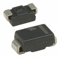
该系列产品符合JEDEC注册的封装外形(JEDEC DO-214AC),为单向和双向类型,其中带色的环表示阴极(单向类型)。

### 参数特性 - 峰值脉冲功率耗散:600W(10/1000μs脉冲)和4kW(8/20μs脉冲)。 - 独立电压范围:从5V到188V。 - 工作结温范围:-55°C至+175°C。 - 漏电流:25°C时0.2μA,85°C时1μA。 - 热阻:结到引脚30°C/W,结到环境120°C/W(在推荐的PCB布局上)。

### 功能详解 - 这些二极管旨在保护敏感电路,延长设备使用寿命,具有较低的钳位电压,提供更好的安全边际。

### 应用信息 - 适用于汽车、医疗设备或SMPS等高端设备,这些场合需要低漏电流和高结温性能以确保可靠性和稳定性。

### 封装信息 - 封装类型:JEDEC DO-214AC塑封平面结构,引脚为镀锡,符合MIL-STD-750方法2026的可焊性。 - 尺寸:提供详细的机械尺寸图表,包括A1、A2、b、c、D、E、E1和L等参数。 - 标记信息:包括阴极条(单向设备)和标记编码,如6UA、6BA等。 - 环保包装:ST提供ECOPACK®包装,符合无铅二次互连的环保要求。
SMA6J85A-TR 价格&库存

很抱歉,暂时无法提供与“SMA6J85A-TR”相匹配的价格&库存,您可以联系我们找货

免费人工找货
SMA6J85A-TR
  •  国内价格 香港价格
  • 1+2.878731+0.35864
  • 10+2.0933310+0.26080

库存:3933

SMA6J85A-TR
  •  国内价格 香港价格
  • 5000+1.715745000+0.21375
  • 10000+1.6966710000+0.21138
  • 15000+1.6871415000+0.21019
  • 20000+1.6680820000+0.20782

库存:0

SMA6J85A-TR
  •  国内价格
  • 1+0.66680
  • 200+0.55570
  • 500+0.44460
  • 1000+0.37050

库存:0

SMA6J85A-TR
  •  国内价格 香港价格
  • 5000+1.711305000+0.21320

库存:3933