®
SMBYW01-200
HIGH EFFICIENCY FAST RECOVERY DIODE
MAIN PRODUCT CHARACTERISTICS IF(AV) VRRM VF(max) Tj (max) 1A 200 V 0.71 V 150 °C
FEATURES AND BENEFITS VERY LOW SWITCHING LOSSES LOW FORWARD VOLTAGE DROP BIPOLAR DEVICE LOW PEAK FORWARD VOLTAGE FOR TELECOM TRANSIENT OPERATION SUCH AS IN LIGHTING PROTECTION CIRCUITS DESCRIPTION Single chip rectifier suited to Switch Mode Power Supplies and high frequency DC to DC converters. Packaged in SMB, this surface mount device is intended for use in low voltage, high frequency inverters, free wheeling and polarity protection applications.
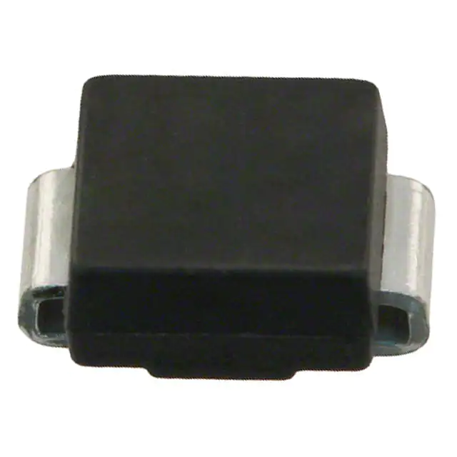
SMB (JEDEC DO-214AA)
ABSOLUTE RATINGS (limiting values) Symbol VRRM IF(RMS) IF(AV) IFSM Tstg Tj Parameter Repetitive peak reverse voltage RMS forward current Average forward current Surge non repetitive forward current Storage and junction temperature range Maximum operating junction temperature Tlead=140°C δ = 0.5 tp=10ms sinusoidal Value 200 8 1 60 - 65 to + 150 150 Unit V A A A °C °C
October 1999 - Ed: 4A
1/5
�SMBYW01-200
THERMAL RESISTANCES Symbol Rth (j-l) Junction to lead Parameter Value 13 Unit °C/W
STATIC ELECTRICAL CHARACTERISTICS Symbol VF * Parameters Forward voltage drop Test Conditions Tj = 25°C Tj = 150°C IR ** Reverse leakage current Tj = 25°C Tj = 125°C
Pulse test : * tp = 380 µs, δ < 2 % ** tp = 5 ms, δ < 2 %
Min.
Typ.
Max. 0.9
Unit V
IF = 1 A IF = 1 A VR = VRRM 180 0.65
0.71 3 400 µA
To evaluate the maximum conduction losses use the following equation : P = 0.58 x IF(AV) + 0.118 x IF2(RMS)
RECOVERY CHARACTERISTICS Symbol trr Tj = 25°C Test Conditions IF = 0.5 A IF = 1 A tfr VFP Tj = 25°C Tj = 25°C IF = 1A IF = 1A Irr = 0.25 A IR = 1A dIF/dt = - 50 A/µs VR = 30V dIF/dt = 100 A/µs dIF/dt = 100 A/µs 25 Min. Typ. Max. 25 35 25 5 ns V Unit ns
2/5
�SMBYW01-200
Fig. 1: Average forward power dissipation versus average forward current .
PF(av)(W) 1.0 0.9 0.8 0.7 0.6 0.5 0.4 0.3 0.2 0.1 0.0 0.0
δ = 0.05 δ = 0.1 δ = 0.2 δ = 0.5
Fig. 2: Peak current versus form factor.
IM(A) 10 9 8 7 6 5 4 3 2 1 0 0.0
P=1.5W P=1.0W P=0.5W P=0.25W
δ=1
IF(av) (A) 0.2 0.4 0.6 0.8 1.0 1.2
0.1
0.2
0.3
0.4
δ
0.5
0.6
0.7
0.8
0.9
1.0
Fig. 3: Average forward current versus ambient temperature (δ=0.5).
IF(av)(A) 1.2
Rth(j-a)=Rth(j-l)
Fig. 4: Non repetitive surge peak forward current versus overload duration.
IM(A) 8 7 6 5
Rth(j-a)=100°C/W
Ta=25°C
1.0 0.8 0.6 0.4 0.2 Tamb(°C) 0.0 0 25 50 75 100 125 150
Ta=50°C
4 3 2 1E-3 1E-2
Ta=75°C
t(s) 1E-1 1E+0
Fig. 5: Variation of thermal impedance junction to ambient versus pulse duration (recommended pad layout, epoxy FR4, e(Cu)=35µm).
Zth(j-a)(°C/W) 1.00
δ = 0.5 δ = 0.2
Fig 6: Forward voltage drop versus forward current (maximum values).
VFM(V) 50.00 10.00
Tj=125°C
0.10
δ = 0.1
1.00
Tj=25°C
Single pulse
0.10
tp(s)
0.01 1E-2
IFM(A)
1E+1 1E+2 5E+2
1E-1
1E+0
0.01 0.0
0.4
0.8
1.2
1.6
2.0
2.4
3/5
�SMBYW01-200
Fig. 7: Junction capacitance versus reverse voltage applied (typical values).
C(pF) 12 10 8 6 4 2 VR(V) 0 1 10 100 200
F=1MHz Tj=25°C
Fig. 8: Reverse recovery current versus dIF/dt .
IRM(A) 6 5 4 3 2 1 dIF/dt(A/µs) 0 0 20 40 60 80 100 120 140 160 180 200
IF=IF(av) 90% confidence Tj=125°C
Fig. 9: Reverse recovery time versus dIF/dt.
Fig. 10: Reverse recovery charges versus dIF/dt.
trr(ns) 100 90 80 70 60 50 40 30 20 10 0
IF=IF(av) 90% confidence Tj=125°C
Qrr(nC) 100 90 80 70 60 50 40 30 20 10 0
IF=IF(av) 90% confidence Tj=125°C
dIF/dt(A/µs) 0 20 40 60 80 100 120 140 160 180 200
dIF/dt(A/µs) 0 20 40 60 80 100 120 140 160 180 200
Fig. 11: Dynamic parameters versus junction temperature.
Fig. 12: Thermal resistance junction to ambient versus copper surface under each lead (Epoxy printed circuit board FR4, copper thickness: 35µm)
Qrr;IRM[Tj] / Qrr;IRM[Tj=125°C] 1.25 1.00
Rth(j-a) (°C/W) 120 100 80
IRM
0.75
Qrr
60 40 20
Tj(°C)
0.50 0.25
S(Cu) (cm²)
100 125 150
0
25
50
75
0
0
1
2
3
4
5
4/5
�SMBYW01-200
PACKAGE MECHANICAL DATA SMB
E1
DIMENSIONS REF.
D
Millimeters Min. Max. 2.45 0.20 2.20 0.41 5.60 4.60 3.95 1.60
Inches Min. 0.075 0.002 0.077 0.006 0.201 0.159 0.130 0.030 Max. 0.096 0.008 0.087 0.016 0.220 0.181 0.156 0.063
E
A1 A2 b c
A1
1.90 0.05 1.95 0.15 5.10 4.05 3.30 0.75
C L
A2
E E1 D L
b
FOOT PRINT DIMENSIONS (in millimeters) SMB (Plastic)
2.3
1.52
2.75
1.52
Ordering type SMBYW01-200
Marking B20
Package SMB
Weight 0.11g
Base qty 2500
Delivery mode Tape & reel
Band indicates cathode Epoxy meets UL94,V0
Information furnished is believed to be accurate and reliable. However, STMicroelectronics assumes no responsibility for the consequences of use of such information nor for any infringement of patents or other rights of third parties which may result from its use. No license is granted by implication or otherwise under any patent or patent rights of STMicroelectronics. Specifications mentioned in this publication are subject to change without notice. This publication supersedes and replaces all information previously supplied. STMicroelectronics products are not authorized for use as critical components in life support devices or systems without express written approval of STMicroelectronics.
The ST logo is a registered trademark of STMicroelectronics © 1999 STMicroelectronics - Printed in Italy - All rights reserved. STMicroelectronics GROUP OF COMPANIES Australia - Brazil - China - Finland - France - Germany - Hong Kong - India - Italy - Japan - Malaysia Malta - Morocco - Singapore - Spain - Sweden - Switzerland - United Kingdom - U.S.A. http://www.st.com
5/5
�
很抱歉,暂时无法提供与“SMBYW01-200”相匹配的价格&库存,您可以联系我们找货
免费人工找货