SPC56AP60x, SPC56AP54x
SPC560P60x, SPC560P54x
32-bit Power Architecture® based MCU with 1088KB Flash memory
and 80KB RAM for automotive chassis and safety applications
Datasheet - production data
General purpose I/Os (80 GPIO + 26 GPI on
LQFP144; 49 GPIO + 16 GPI on LQFP100)
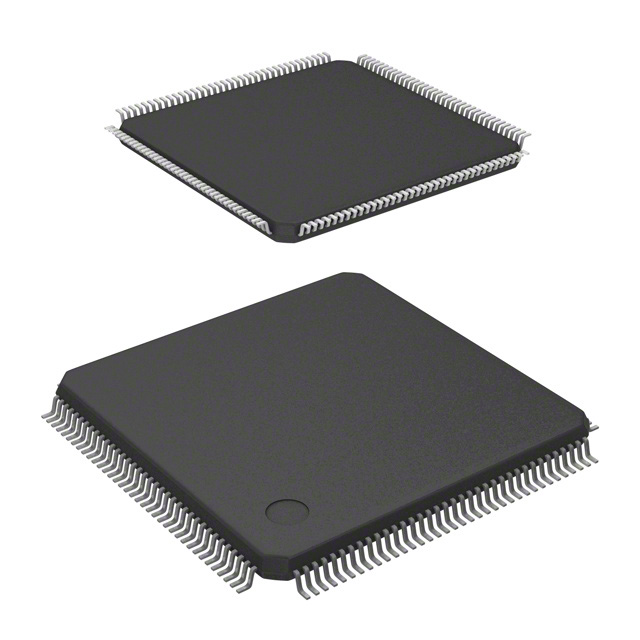
LQFP100
14 x 14 mm
2 general purpose eTimer units
– 6 timers, each with up/down count
capabilities
– 16-bit resolution, cascadable counters
– Quadrature decode with rotation direction
flag
– Double buffer input capture and output
compare
LQFP144
20 x 20 mm
Features
AEC-Q10x qualified
64 MHz, single issue, 32-bit CPU core complex
(e200z0h)
– Compliant with Power Architecture®
embedded category
– Variable Length Encoding (VLE)
Memory organization
– Up to 1024 KB on-chip code Flash memory
with additional 64 KB for EEPROM
emulation (data flash), with ECC, with
erase/program controller
– Up to 80 KB on-chip SRAM with ECC
Fail safe protection
– ECC protection on system SRAM and
Flash
– Safety port
– SWT with servicing sequence pseudorandom generator
– Power management
– Non-maskable interrupt for both cores
– Fault collection and control unit (FCCU)
– Safe mode of system-on-chip (SoC)
– Register protection scheme
Nexus® L2+ interface
Single 3.3 V or 5 V supply for I/Os and ADC
Communications interfaces
– 2 LINFlex modules (LIN 2.1,
1 × Master/Slave, 1 × Master Only)
– 5 DSPI modules with automatic chip select
generation
– 2 FlexCAN interfaces (2.0B Active) with 32
message buffers
– 1 Safety port based on FlexCAN; usable as
third CAN when not used as safety port
– 1 FlexRay™ module (V2.1) with dual or
single channel, 64 message buffers and up
to 10 Mbit/s
2 CRC units with three contexts and 3
hardwired polynomials(CRC8,CRC32 and
CRC-16-CCITT)
10-bit A/D converter
– 27 input channels and pre-sampling feature
– Conversion time < 1 µs including sampling
time at full precision
– Programmable cross triggering unit (CTU)
– 4 analog watchdog with interrupt capability
On-chip CAN/UART Bootstrap loader with boot
assist module (BAM)
Ambient temperature ranges: –40 to 125 °C or
–40 to 105 °C
2 on-platform peripherals set with 2 INTC
16-channel eDMA controller with multiple
transfer request sources
June 2016
This is information on a product in full production.
DocID18340 Rev 6
1/105
www.st.com
�SPC56xP54x, SPC56xP60x
Table 1. Device summary
Part number
Package
2/105
768 KB Flash
1 MB Flash
LQFP144
SPC560P54L5
SPC56AP54L5
SPC560P60L5
SPC56AP60L5
LQFP100
SPC560P54L3
SPC56AP54L3
SPC560P60L3
SPC56AP60L3
DocID18340 Rev 6
�SPC56xP54x, SPC56xP60x
Contents
Contents
1
Introduction . . . . . . . . . . . . . . . . . . . . . . . . . . . . . . . . . . . . . . . . . . . . . . . . 8
1.1
Document overview . . . . . . . . . . . . . . . . . . . . . . . . . . . . . . . . . . . . . . . . . . 8
1.2
Description . . . . . . . . . . . . . . . . . . . . . . . . . . . . . . . . . . . . . . . . . . . . . . . . . 8
1.3
Device comparison . . . . . . . . . . . . . . . . . . . . . . . . . . . . . . . . . . . . . . . . . . . 8
1.4
Block diagram . . . . . . . . . . . . . . . . . . . . . . . . . . . . . . . . . . . . . . . . . . . . . . 10
1.5
Feature details . . . . . . . . . . . . . . . . . . . . . . . . . . . . . . . . . . . . . . . . . . . . . 14
1.5.1
High performance e200z0h core processor . . . . . . . . . . . . . . . . . . . . . . 14
1.5.2
Crossbar switch (XBAR) . . . . . . . . . . . . . . . . . . . . . . . . . . . . . . . . . . . . 14
1.5.3
Enhanced direct memory access (eDMA) . . . . . . . . . . . . . . . . . . . . . . . 15
1.5.4
On-chip flash memory with ECC . . . . . . . . . . . . . . . . . . . . . . . . . . . . . . 15
1.5.5
On-chip SRAM with ECC . . . . . . . . . . . . . . . . . . . . . . . . . . . . . . . . . . . . 16
1.5.6
Interrupt controller (INTC) . . . . . . . . . . . . . . . . . . . . . . . . . . . . . . . . . . . 16
1.5.7
System clocks and clock generation . . . . . . . . . . . . . . . . . . . . . . . . . . . 17
1.5.8
Frequency modulated phase-locked loop (FMPLL) . . . . . . . . . . . . . . . . 17
1.5.9
Main oscillator . . . . . . . . . . . . . . . . . . . . . . . . . . . . . . . . . . . . . . . . . . . . 18
1.5.10
Internal RC oscillator . . . . . . . . . . . . . . . . . . . . . . . . . . . . . . . . . . . . . . . 18
1.5.11
Periodic interrupt timer (PIT) . . . . . . . . . . . . . . . . . . . . . . . . . . . . . . . . . 18
1.5.12
System timer module (STM) . . . . . . . . . . . . . . . . . . . . . . . . . . . . . . . . . 18
1.5.13
Software watchdog timer (SWT) . . . . . . . . . . . . . . . . . . . . . . . . . . . . . . 19
1.5.14
Fault collection and control unit (FCCU) . . . . . . . . . . . . . . . . . . . . . . . . 19
1.5.15
System integration unit (SIUL) . . . . . . . . . . . . . . . . . . . . . . . . . . . . . . . . 19
1.5.16
Boot and censorship . . . . . . . . . . . . . . . . . . . . . . . . . . . . . . . . . . . . . . . 19
1.5.17
Error correction status module (ECSM) . . . . . . . . . . . . . . . . . . . . . . . . . 20
1.5.18
FlexCAN . . . . . . . . . . . . . . . . . . . . . . . . . . . . . . . . . . . . . . . . . . . . . . . . 20
1.5.19
Safety port (FlexCAN) . . . . . . . . . . . . . . . . . . . . . . . . . . . . . . . . . . . . . . 21
1.5.20
FlexRay . . . . . . . . . . . . . . . . . . . . . . . . . . . . . . . . . . . . . . . . . . . . . . . . . 21
1.5.21
Serial communication interface module (LINFlex) . . . . . . . . . . . . . . . . . 22
1.5.22
Deserial serial peripheral interface (DSPI) . . . . . . . . . . . . . . . . . . . . . . 22
1.5.23
eTimer . . . . . . . . . . . . . . . . . . . . . . . . . . . . . . . . . . . . . . . . . . . . . . . . . . 23
1.5.24
Analog-to-digital converter (ADC) . . . . . . . . . . . . . . . . . . . . . . . . . . . . . 24
1.5.25
Cross triggering unit (CTU) . . . . . . . . . . . . . . . . . . . . . . . . . . . . . . . . . . 24
1.5.26
Cyclic redundancy check (CRC) . . . . . . . . . . . . . . . . . . . . . . . . . . . . . . 25
1.5.27
Nexus development interface (NDI) . . . . . . . . . . . . . . . . . . . . . . . . . . . . 25
1.5.28
IEEE 1149.1 (JTAG) controller . . . . . . . . . . . . . . . . . . . . . . . . . . . . . . . . 26
DocID18340 Rev 6
3/105
5
�Contents
SPC56xP54x, SPC56xP60x
1.5.29
2
3
Package pinouts and signal descriptions . . . . . . . . . . . . . . . . . . . . . . . 27
2.1
Package pinouts . . . . . . . . . . . . . . . . . . . . . . . . . . . . . . . . . . . . . . . . . . . . 27
2.2
Pin descriptions . . . . . . . . . . . . . . . . . . . . . . . . . . . . . . . . . . . . . . . . . . . . 29
2.2.1
Power supply and reference voltage pins . . . . . . . . . . . . . . . . . . . . . . . 29
2.2.2
System pins . . . . . . . . . . . . . . . . . . . . . . . . . . . . . . . . . . . . . . . . . . . . . . 31
2.2.3
Pin muxing . . . . . . . . . . . . . . . . . . . . . . . . . . . . . . . . . . . . . . . . . . . . . . . 33
Electrical characteristics . . . . . . . . . . . . . . . . . . . . . . . . . . . . . . . . . . . . 48
3.1
Introduction . . . . . . . . . . . . . . . . . . . . . . . . . . . . . . . . . . . . . . . . . . . . . . . 48
3.2
Parameter classification . . . . . . . . . . . . . . . . . . . . . . . . . . . . . . . . . . . . . . 48
3.3
Absolute maximum ratings . . . . . . . . . . . . . . . . . . . . . . . . . . . . . . . . . . . . 49
3.4
Recommended operating conditions . . . . . . . . . . . . . . . . . . . . . . . . . . . . 51
3.5
Thermal characteristics . . . . . . . . . . . . . . . . . . . . . . . . . . . . . . . . . . . . . . 55
3.5.1
General notes for specifications at maximum junction temperature . . . 56
3.6
Electromagnetic interference (EMI) characteristics . . . . . . . . . . . . . . . . . 58
3.7
Electrostatic discharge (ESD) characteristics . . . . . . . . . . . . . . . . . . . . . 58
3.8
Power management electrical characteristics . . . . . . . . . . . . . . . . . . . . . 58
3.8.1
Voltage regulator electrical characteristics . . . . . . . . . . . . . . . . . . . . . . 58
3.8.2
Voltage monitor electrical characteristics . . . . . . . . . . . . . . . . . . . . . . . . 60
3.9
Power Up/Down sequencing . . . . . . . . . . . . . . . . . . . . . . . . . . . . . . . . . . 61
3.10
NVUSRO register . . . . . . . . . . . . . . . . . . . . . . . . . . . . . . . . . . . . . . . . . . . 63
3.10.1
3.11
NVUSRO[PAD3V5V] field description . . . . . . . . . . . . . . . . . . . . . . . . . . 63
DC electrical characteristics . . . . . . . . . . . . . . . . . . . . . . . . . . . . . . . . . . . 64
3.11.1
DC electrical characteristics (5 V) . . . . . . . . . . . . . . . . . . . . . . . . . . . . . 64
3.11.2
DC electrical characteristics (3.3 V) . . . . . . . . . . . . . . . . . . . . . . . . . . . . 67
3.11.3
I/O pad current specification . . . . . . . . . . . . . . . . . . . . . . . . . . . . . . . . . 71
3.12
Main oscillator electrical characteristics . . . . . . . . . . . . . . . . . . . . . . . . . . 72
3.13
FMPLL electrical characteristics . . . . . . . . . . . . . . . . . . . . . . . . . . . . . . . . 73
3.14
16 MHz RC oscillator electrical characteristics . . . . . . . . . . . . . . . . . . . . 74
3.15
Analog-to-Digital converter (ADC) electrical characteristics . . . . . . . . . . . 74
3.16
4/105
On-chip voltage regulator (VREG) . . . . . . . . . . . . . . . . . . . . . . . . . . . . . 26
3.15.1
Input impedance and ADC accuracy . . . . . . . . . . . . . . . . . . . . . . . . . . . 75
3.15.2
ADC conversion characteristics . . . . . . . . . . . . . . . . . . . . . . . . . . . . . . . 80
Flash memory electrical characteristics . . . . . . . . . . . . . . . . . . . . . . . . . . 81
DocID18340 Rev 6
�SPC56xP54x, SPC56xP60x
3.17
AC specifications . . . . . . . . . . . . . . . . . . . . . . . . . . . . . . . . . . . . . . . . . . . 83
3.17.1
3.18
4
Contents
Pad AC specifications . . . . . . . . . . . . . . . . . . . . . . . . . . . . . . . . . . . . . . 83
AC timing characteristics . . . . . . . . . . . . . . . . . . . . . . . . . . . . . . . . . . . . . 83
3.18.1
RESET pin characteristics . . . . . . . . . . . . . . . . . . . . . . . . . . . . . . . . . . . 83
3.18.2
IEEE 1149.1 interface timing . . . . . . . . . . . . . . . . . . . . . . . . . . . . . . . . . 86
3.18.3
Nexus timing . . . . . . . . . . . . . . . . . . . . . . . . . . . . . . . . . . . . . . . . . . . . . 88
3.18.4
External interrupt timing (IRQ pin) . . . . . . . . . . . . . . . . . . . . . . . . . . . . . 90
3.18.5
DSPI timing . . . . . . . . . . . . . . . . . . . . . . . . . . . . . . . . . . . . . . . . . . . . . . 91
Package characteristics . . . . . . . . . . . . . . . . . . . . . . . . . . . . . . . . . . . . . 97
4.1
ECOPACK® . . . . . . . . . . . . . . . . . . . . . . . . . . . . . . . . . . . . . . . . . . . . . . . 97
4.2
Package mechanical data . . . . . . . . . . . . . . . . . . . . . . . . . . . . . . . . . . . . 97
4.2.1
LQFP144 mechanical outline drawing . . . . . . . . . . . . . . . . . . . . . . . . . . 97
4.2.2
LQFP100 mechanical outline drawing . . . . . . . . . . . . . . . . . . . . . . . . . . 99
5
Ordering information . . . . . . . . . . . . . . . . . . . . . . . . . . . . . . . . . . . . . . 101
6
Revision history . . . . . . . . . . . . . . . . . . . . . . . . . . . . . . . . . . . . . . . . . . 102
DocID18340 Rev 6
5/105
5
�List of tables
SPC56xP54x, SPC56xP60x
List of tables
Table 1.
Table 2.
Table 3.
Table 4.
Table 5.
Table 6.
Table 7.
Table 8.
Table 9.
Table 10.
Table 11.
Table 12.
Table 13.
Table 14.
Table 15.
Table 16.
Table 17.
Table 18.
Table 19.
Table 20.
Table 21.
Table 22.
Table 23.
Table 24.
Table 25.
Table 26.
Table 27.
Table 28.
Table 29.
Table 30.
Table 31.
Table 32.
Table 33.
Table 34.
Table 35.
Table 36.
Table 37.
Table 38.
Table 39.
Table 40.
Table 41.
Table 42.
Table 43.
Table 44.
6/105
Device summary . . . . . . . . . . . . . . . . . . . . . . . . . . . . . . . . . . . . . . . . . . . . . . . . . . . . . . . . . . 2
SPC56xP54x/SPC56xP60x device comparison . . . . . . . . . . . . . . . . . . . . . . . . . . . . . . . . . . 8
SPC56xP54x/SPC56xP60x device configuration difference . . . . . . . . . . . . . . . . . . . . . . . 10
SPC56xP54x/SPC56xP60x series block summary . . . . . . . . . . . . . . . . . . . . . . . . . . . . . . 12
Supply pins . . . . . . . . . . . . . . . . . . . . . . . . . . . . . . . . . . . . . . . . . . . . . . . . . . . . . . . . . . . . . 29
System pins . . . . . . . . . . . . . . . . . . . . . . . . . . . . . . . . . . . . . . . . . . . . . . . . . . . . . . . . . . . . 31
Pin muxing . . . . . . . . . . . . . . . . . . . . . . . . . . . . . . . . . . . . . . . . . . . . . . . . . . . . . . . . . . . . . 33
Parameter classifications . . . . . . . . . . . . . . . . . . . . . . . . . . . . . . . . . . . . . . . . . . . . . . . . . . 48
Absolute maximum ratings . . . . . . . . . . . . . . . . . . . . . . . . . . . . . . . . . . . . . . . . . . . . . . . . . 49
Recommended operating conditions (5.0 V) . . . . . . . . . . . . . . . . . . . . . . . . . . . . . . . . . . . 51
Recommended operating conditions (3.3 V) . . . . . . . . . . . . . . . . . . . . . . . . . . . . . . . . . . . 52
Thermal characteristics for 144-pin LQFP . . . . . . . . . . . . . . . . . . . . . . . . . . . . . . . . . . . . . 55
Thermal characteristics for 100-pin LQFP . . . . . . . . . . . . . . . . . . . . . . . . . . . . . . . . . . . . . 56
EMI testing specifications . . . . . . . . . . . . . . . . . . . . . . . . . . . . . . . . . . . . . . . . . . . . . . . . . . 58
ESD ratings. . . . . . . . . . . . . . . . . . . . . . . . . . . . . . . . . . . . . . . . . . . . . . . . . . . . . . . . . . . . . 58
Approved NPN ballast components . . . . . . . . . . . . . . . . . . . . . . . . . . . . . . . . . . . . . . . . . . 59
Voltage regulator electrical characteristics . . . . . . . . . . . . . . . . . . . . . . . . . . . . . . . . . . . . . 60
Low voltage monitor electrical characteristics. . . . . . . . . . . . . . . . . . . . . . . . . . . . . . . . . . . 61
PAD3V5V field description . . . . . . . . . . . . . . . . . . . . . . . . . . . . . . . . . . . . . . . . . . . . . . . . . 63
DC electrical characteristics (5.0 V, NVUSRO[PAD3V5V]=0) . . . . . . . . . . . . . . . . . . . . . . 64
Supply current (5.0 V, NVUSRO[PAD3V5V]=0) . . . . . . . . . . . . . . . . . . . . . . . . . . . . . . . . . 66
DC electrical characteristics (3.3 V, NVUSRO[PAD3V5V]=1) . . . . . . . . . . . . . . . . . . . . . . 67
Supply current (3.3 V, NVUSRO[PAD3V5V]=1) . . . . . . . . . . . . . . . . . . . . . . . . . . . . . . . . . 69
Peripherals supply current (5 V and 3.3 V) . . . . . . . . . . . . . . . . . . . . . . . . . . . . . . . . . . . . . 70
I/O supply segment . . . . . . . . . . . . . . . . . . . . . . . . . . . . . . . . . . . . . . . . . . . . . . . . . . . . . . . 71
I/O consumption . . . . . . . . . . . . . . . . . . . . . . . . . . . . . . . . . . . . . . . . . . . . . . . . . . . . . . . . . 71
Main oscillator electrical characteristics (5.0 V, NVUSRO[PAD3V5V]=0) . . . . . . . . . . . . . 72
Main oscillator electrical characteristics (3.3 V, NVUSRO[PAD3V5V]=1) . . . . . . . . . . . . . 72
Input clock characteristics. . . . . . . . . . . . . . . . . . . . . . . . . . . . . . . . . . . . . . . . . . . . . . . . . . 73
PLLMRFM electrical specifications (VDDPLL = 1.08 V to 1.32 V, VSS = VSSPLL = 0 V, TA = TL
to TH) . . . . . . . . . . . . . . . . . . . . . . . . . . . . . . . . . . . . . . . . . . . . . . . . . . . . . . . . . . . . . . . . . 73
16 MHz RC oscillator electrical characteristics . . . . . . . . . . . . . . . . . . . . . . . . . . . . . . . . . . 74
ADC conversion characteristics . . . . . . . . . . . . . . . . . . . . . . . . . . . . . . . . . . . . . . . . . . . . . 80
Program and erase specifications . . . . . . . . . . . . . . . . . . . . . . . . . . . . . . . . . . . . . . . . . . . 81
Flash memory module life. . . . . . . . . . . . . . . . . . . . . . . . . . . . . . . . . . . . . . . . . . . . . . . . . . 82
Flash read access timing . . . . . . . . . . . . . . . . . . . . . . . . . . . . . . . . . . . . . . . . . . . . . . . . . . 82
Output pin transition times . . . . . . . . . . . . . . . . . . . . . . . . . . . . . . . . . . . . . . . . . . . . . . . . . 83
RESET electrical characteristics. . . . . . . . . . . . . . . . . . . . . . . . . . . . . . . . . . . . . . . . . . . . . 85
JTAG pin AC electrical characteristics . . . . . . . . . . . . . . . . . . . . . . . . . . . . . . . . . . . . . . . . 86
Nexus debug port timing . . . . . . . . . . . . . . . . . . . . . . . . . . . . . . . . . . . . . . . . . . . . . . . . . . . 88
External interrupt timing . . . . . . . . . . . . . . . . . . . . . . . . . . . . . . . . . . . . . . . . . . . . . . . . . . . 90
DSPI timing . . . . . . . . . . . . . . . . . . . . . . . . . . . . . . . . . . . . . . . . . . . . . . . . . . . . . . . . . . . . . 91
LQFP144 mechanical data . . . . . . . . . . . . . . . . . . . . . . . . . . . . . . . . . . . . . . . . . . . . . . . . . 98
LQFP100 mechanical data . . . . . . . . . . . . . . . . . . . . . . . . . . . . . . . . . . . . . . . . . . . . . . . . . 99
Document revision history . . . . . . . . . . . . . . . . . . . . . . . . . . . . . . . . . . . . . . . . . . . . . . . . 102
DocID18340 Rev 6
�SPC56xP54x, SPC56xP60x
List of figures
List of figures
Figure 1.
Figure 2.
Figure 3.
Figure 4.
Figure 5.
Figure 6.
Figure 7.
Figure 8.
Figure 9.
Figure 10.
Figure 11.
Figure 12.
Figure 13.
Figure 14.
Figure 15.
Figure 16.
Figure 17.
Figure 18.
Figure 19.
Figure 20.
Figure 21.
Figure 22.
Figure 23.
Figure 24.
Figure 25.
Figure 26.
Figure 27.
Figure 28.
Figure 29.
Figure 30.
Figure 31.
Figure 32.
Figure 33.
Figure 34.
Figure 35.
Figure 36.
Figure 37.
Figure 38.
Figure 39.
Figure 40.
SPC56xP54x/SPC56xP60x block diagram. . . . . . . . . . . . . . . . . . . . . . . . . . . . . . . . . . . . . 11
LQFP176 pinout (top view) . . . . . . . . . . . . . . . . . . . . . . . . . . . . . . . . . . . . . . . . . . . . . . . . . 27
LQFP144 pinout (top view) . . . . . . . . . . . . . . . . . . . . . . . . . . . . . . . . . . . . . . . . . . . . . . . . . 28
LQFP100 pinout (top view) . . . . . . . . . . . . . . . . . . . . . . . . . . . . . . . . . . . . . . . . . . . . . . . . . 29
Power supplies constraints . . . . . . . . . . . . . . . . . . . . . . . . . . . . . . . . . . . . . . . . . . . . . . . . . 50
Independent ADC supply . . . . . . . . . . . . . . . . . . . . . . . . . . . . . . . . . . . . . . . . . . . . . . . . . . 51
Power supplies constraints . . . . . . . . . . . . . . . . . . . . . . . . . . . . . . . . . . . . . . . . . . . . . . . . . 54
Independent ADC supply . . . . . . . . . . . . . . . . . . . . . . . . . . . . . . . . . . . . . . . . . . . . . . . . . . 55
Voltage regulator configuration . . . . . . . . . . . . . . . . . . . . . . . . . . . . . . . . . . . . . . . . . . . . . . 59
Power-up typical sequence. . . . . . . . . . . . . . . . . . . . . . . . . . . . . . . . . . . . . . . . . . . . . . . . . 62
Power-down typical sequence . . . . . . . . . . . . . . . . . . . . . . . . . . . . . . . . . . . . . . . . . . . . . . 62
Brown-out typical sequence . . . . . . . . . . . . . . . . . . . . . . . . . . . . . . . . . . . . . . . . . . . . . . . . 63
I/O input DC electrical characteristics definition . . . . . . . . . . . . . . . . . . . . . . . . . . . . . . . . . 64
I/O input DC electrical characteristics definition . . . . . . . . . . . . . . . . . . . . . . . . . . . . . . . . . 67
ADC characteristics and error definitions . . . . . . . . . . . . . . . . . . . . . . . . . . . . . . . . . . . . . . 75
Input equivalent circuit (precise channels) . . . . . . . . . . . . . . . . . . . . . . . . . . . . . . . . . . . . . 76
Input equivalent circuit (extended channels) . . . . . . . . . . . . . . . . . . . . . . . . . . . . . . . . . . . 77
Transient behavior during sampling phase . . . . . . . . . . . . . . . . . . . . . . . . . . . . . . . . . . . . . 77
Spectral representation of input signal . . . . . . . . . . . . . . . . . . . . . . . . . . . . . . . . . . . . . . . . 79
Start-up reset requirements . . . . . . . . . . . . . . . . . . . . . . . . . . . . . . . . . . . . . . . . . . . . . . . . 84
Noise filtering on reset signal . . . . . . . . . . . . . . . . . . . . . . . . . . . . . . . . . . . . . . . . . . . . . . . 84
JTAG test clock input timing . . . . . . . . . . . . . . . . . . . . . . . . . . . . . . . . . . . . . . . . . . . . . . . . 86
JTAG test access port timing . . . . . . . . . . . . . . . . . . . . . . . . . . . . . . . . . . . . . . . . . . . . . . . 87
JTAG boundary scan timing . . . . . . . . . . . . . . . . . . . . . . . . . . . . . . . . . . . . . . . . . . . . . . . . 88
Nexus output timing . . . . . . . . . . . . . . . . . . . . . . . . . . . . . . . . . . . . . . . . . . . . . . . . . . . . . . 89
Nexus event trigger and test clock timings . . . . . . . . . . . . . . . . . . . . . . . . . . . . . . . . . . . . . 89
Nexus TDI, TMS, TDO timing . . . . . . . . . . . . . . . . . . . . . . . . . . . . . . . . . . . . . . . . . . . . . . . 90
External interrupt timing . . . . . . . . . . . . . . . . . . . . . . . . . . . . . . . . . . . . . . . . . . . . . . . . . . . 91
DSPI classic SPI timing — master, CPHA = 0 . . . . . . . . . . . . . . . . . . . . . . . . . . . . . . . . . . 92
DSPI classic SPI timing — master, CPHA = 1 . . . . . . . . . . . . . . . . . . . . . . . . . . . . . . . . . . 93
DSPI classic SPI timing — slave, CPHA = 0 . . . . . . . . . . . . . . . . . . . . . . . . . . . . . . . . . . . 93
DSPI classic SPI timing — slave, CPHA = 1 . . . . . . . . . . . . . . . . . . . . . . . . . . . . . . . . . . . 94
DSPI modified transfer format timing — master, CPHA = 0 . . . . . . . . . . . . . . . . . . . . . . . . 94
DSPI modified transfer format timing — master, CPHA = 1 . . . . . . . . . . . . . . . . . . . . . . . . 95
DSPI modified transfer format timing — slave, CPHA = 0 . . . . . . . . . . . . . . . . . . . . . . . . . 95
DSPI modified transfer format timing — slave, CPHA = 1 . . . . . . . . . . . . . . . . . . . . . . . . . 96
DSPI PCS strobe (PCSS) timing . . . . . . . . . . . . . . . . . . . . . . . . . . . . . . . . . . . . . . . . . . . . 96
LQFP144 package mechanical drawing . . . . . . . . . . . . . . . . . . . . . . . . . . . . . . . . . . . . . . . 97
LQFP100 package mechanical drawing . . . . . . . . . . . . . . . . . . . . . . . . . . . . . . . . . . . . . . . 99
Ordering information scheme . . . . . . . . . . . . . . . . . . . . . . . . . . . . . . . . . . . . . . . . . . . . . . 101
DocID18340 Rev 6
7/105
7
�Introduction
SPC56xP54x, SPC56xP60x
1
Introduction
1.1
Document overview
This document provides electrical specifications, pin assignments, and package diagrams
for the SPC56xP54x/SPC56xP60x series of microcontroller units (MCUs). It also describes
the device features and highlights important electrical and physical characteristics. For
functional characteristics, refer to the device reference manual.
1.2
Description
This 32-bit system-on-chip (SoC) automotive microcontroller family is the latest
achievement in integrated automotive application controllers. It belongs to an expanding
range of automotive-focused products designed to address chassis applications specifically
the airbag application.
This family is one of a series of next-generation integrated automotive microcontrollers
based on the Power Architecture technology.
The advanced and cost-efficient host processor core of this automotive controller family
complies with the Power Architecture embedded category. It operates up to 64 MHz and
offers high performance processing optimized for low power consumption. It capitalizes on
the available development infrastructure of current Power Architecture devices and is
supported with software drivers, operating systems and configuration code to assist with
users implementations.
1.3
Device comparison
Table 2 provides a summary of different members of the SPC56xP54x/SPC56xP60x family
and their features—relative to Full-featured version—to enable a comparison among the
family members and an understanding of the range of functionality offered within this family.
Table 2. SPC56xP54x/SPC56xP60x device comparison
Feature
Code Flash memory (with ECC)
SPC560P54
SPC560P60
SPC56AP54
SPC56AP60
768 KB
1 MB
768 KB
1 MB
64 KB
80 KB
Data Flash / EE (with ECC)
SRAM (with ECC)
Processor core
64 KB
64 KB
80 KB
32-bit e200z0h
Instruction set
VLE
CPU performance
0-64 MHz
FMPLL (frequency-modulated phaselocked loop) modules
1
INTC (interrupt controller) channels
PIT (periodic interrupt timer)
8/105
32-bit Dual e200z0h
148
1 (includes four 32-bit timers)
DocID18340 Rev 6
�SPC56xP54x, SPC56xP60x
Introduction
Table 2. SPC56xP54x/SPC56xP60x device comparison (continued)
Feature
SPC560P54
SPC560P60
Enhanced DMA (direct memory
access) channels
SPC56AP54
16
FlexRay
Yes (64 message buffer)
3(1),(2)
FlexCAN (controller area network)
Safety port
Yes (via third FlexCAN module)
Yes(3)
FCCU (fault collection and control unit)
CTU (cross triggering unit)
Yes
eTimer channels
2×6
FlexPWM (pulse-width modulation)
channels
No
Analog-to-digital converters (ADC)
One (10-bit, 27-channel)(4)
LINFlex modules
2 (1 × Master/Slave, 1 × Master only)(5)
DSPI (deserial serial peripheral
interface) modules
5(6)
CRC (cyclic redundancy check) units
2(7)
JTAG interface
Yes
Yes (Level 2+)(8)
Nexus port controller (NPC)
Digital power supply(9)
Supply
3.3 V or 5 V single supply with external transistor
Analog power supply
3.3 V or 5 V
Internal RC oscillator
16 MHz
External crystal oscillator
4–40 MHz
LQFP100
LQFP144
Packages
Temperature
SPC56AP60
Standard ambient
temperature
LQFP100
LQFP144
LQFP176(10)
–40 to 125 °C
1. Each FlexCAN module has 32 message buffers.
2. One FlexCAN module can act as a Safety Port with a bit rate as high as 7.5 Mbit/s.
3. Enhanced FCCU version.
4. Same amount of ADC channels as on SPC560P44/50 not considering the internally connected ones. 26 channels on
LQFP144 and 16 channels on LQFP100.
5. LinFlex_1 is Master Only.
6. Increased number of CS for DSPI_1.
7. Upgraded specification with addition of 8-bits polynomial (CRC-8 VDA CAN) support and 3rd context.
8. Improved debugging capability with data trace capability and increased Nexus throughput available on emulation package.
9. 3.3 V range and 5 V range correspond to different orderable parts.
10. Software development package only. Not available for production.
DocID18340 Rev 6
9/105
104
�Introduction
SPC56xP54x, SPC56xP60x
SPC56xP54x/SPC56xP60x is present on the market in two different options enabling
different features: Full-featured, and Airbag configuration. Table 3 shows the main
differences between the two versions.
Table 3. SPC56xP54x/SPC56xP60x device configuration difference
Feature
FlexCAN (controller area network)
Enhanced
Full-featured
Full-featured
Airbag
3
2
2
CTU (cross triggering unit)
Yes
No
Yes (64 message buffer)
No
DSPI (deserial serial peripheral interface) modules
5
4
CRC (cyclic redundancy check) unit
2
1
FlexRay
1.4
Block diagram
Figure 1 shows a top-level block diagram of the SPC56xP54x/SPC56xP60x MCU. Table 4
summarizes the functions of the blocks.
10/105
DocID18340 Rev 6
�SPC56xP54x, SPC56xP60x
Introduction
Figure 1. SPC56xP54x/SPC56xP60x block diagram
e200z0 Core
PMU
INTC_0
SWT_0
STM_0
e200z0 Core
32-bit
general
purpose
registers
Variable
Exception
length
handler
encoded
instructions
32-bit
general
purpose
registers
Variable
Exception
length
handler
encoded
instructions
INTC_1
Special
purpose
registers
Integer
Instruction
execution
unit
unit
Special
purpose
registers
Integer
Instruction
execution
unit
unit
SWT_1
Branch
prediction
unit
Load/Store
unit
ECSM_0
Nexus 2+
INSTR
STM_1
JTAG
ECSM_1
Nexus
port
controller
SEMA4_0
DMAMUX_0
Branch
prediction
unit
Load/Store
unit
JTAG
Nexus 2+
SEMA4_1
DATA
INSTR
DATA
DMA_0
M2
M3
M0
M1
M5
M6
Cross Bar Switch (XBAR, AMBA 2.0 v6 AHB) XBAR_0
Memory protection unit MPU_0
S7
Memory protection unit MPU_1
S2
S0
S1
NASPS_0
P0
PBRIDGE_0
S6
S3
NASPS_1
P1
PFLASHC_0
PBRIDGE_1
SRAMC_0
1024KB
code flash
with ECC
4x16KB
data flash
with ECC
32KB
SRAM
with ECC
FCCU_0
DSPI_4
FlexCAN_1
MC_RGM
XOSC
FMPLL
IRCOSC
CMU_1
CMU_0
WakeUp
MC_CGM
FlexCAN_0
Peripheral Bus (IPS)
SafetyPort_0
LINFlex_1
LINFlex_0
DSPI_3
DSPI_2
DSPI_1
DSPI_0
eTimer_1
eTimer_0
CTU_0
ADC_0
FlexRay
Peripheral Bus (IPS)
CRC_1
48KB
SRAM
with ECC
MC_ME
SSCM
MC_PCU
PIT
BAM
CRC_0
SIUL
SRAMC_1
26
DocID18340 Rev 6
11/105
104
�Introduction
SPC56xP54x, SPC56xP60x
Table 4. SPC56xP54x/SPC56xP60x series block summary
Block
Function
Analog-to-digital converter (ADC) Multi-channel, 10-bit analog-to-digital converter
Boot assist module (BAM)
Block of read-only memory containing VLE code which is executed according to
the boot mode of the device
Clock generation module
(MC_CGM)
Provides logic and control required for the generation of system and peripheral
clocks
Controller area network
(FlexCAN)
Supports the standard CAN communications protocol
Cross triggering unit (CTU)
Enables synchronization of ADC conversions with a timer event from the
eMIOS or from the PIT
Crossbar switch (XBAR)
Supports simultaneous connections between two master ports and three slave
ports. The crossbar supports a 32-bit address bus width and a 32-bit data bus
width.
Cyclic redundancy checker
(CRC) unit
Is dedicated to the computation of CRC off-loading the CPU. Each context has
a separate CRC computation engine in order to allow the concurrent
computation of the CRC of multiple data streams.
Deserial serial peripheral
interface (DSPI)
Provides a synchronous serial interface for communication with external
devices
Enhanced direct memory access
(eDMA)
Performs complex data transfers with minimal intervention from a host
processor via “n” programmable channels
Enhanced timer (eTimer)
Provides enhanced programmable up/down modulo counting
Error correction status module
(ECSM)
Provides a myriad of miscellaneous control functions for the device including
program-visible information about configuration and revision levels, a reset
status register, wakeup control for exiting sleep modes, and optional features
such as information on memory errors reported by error-correcting codes
External oscillator (XOSC)
Provides an output clock used as input reference for FMPLL_0 or as reference
clock for specific modules depending on system needs
Fault collection and control unit
(FCCU)
Provides functional safety to the device
Flash memory
Provides non-volatile storage for program code, constants and variables
FlexRay (FlexRay communication
Provides high-speed distributed control for advanced automotive applications
controller)
Frequency-modulated phaselocked loop (FMPLL)
Generates high-speed system clocks and supports programmable frequency
modulation
Interrupt controller (INTC)
Provides priority-based preemptive scheduling of interrupt requests
JTAG controller
Provides the means to test chip functionality and connectivity while remaining
transparent to system logic when not in test mode
LINFlex controller
Manages a high number of LIN (Local Interconnect Network protocol)
messages efficiently with a minimum of CPU load
Mode entry module (MC_ME)
Provides a mechanism for controlling the device operational mode and mode
transition sequences in all functional states; also manages the power control
unit, reset generation module and clock generation module, and holds the
configuration, control and status registers accessible for applications
12/105
DocID18340 Rev 6
�SPC56xP54x, SPC56xP60x
Introduction
Table 4. SPC56xP54x/SPC56xP60x series block summary (continued)
Block
Function
Peripheral bridge (PBRIDGE)
Is the interface between the system bus and on-chip peripherals
Periodic interrupt timer (PIT)
Produces periodic interrupts and triggers
Power control unit (MC_PCU)
Reduces the overall power consumption by disconnecting parts of the device
from the power supply via a power switching device; device components are
grouped into sections called “power domains” which are controlled by the PCU
Reset generation module
(MC_RGM)
Centralizes reset sources and manages the device reset sequence of the
device
Semaphore unit (SEMA4)
Provides the hardware support needed in multi-core systems for implementing
semaphores and provide a simple mechanism to achieve lock/unlock
operations via a single write access
Static random-access memory
(SRAM)
Provides storage for program code, constants, and variables
Provides control over all the electrical pad controls and up 32 ports with 16 bits
System integration unit lite (SIUL) of bidirectional, general-purpose input and output signals and supports up to 32
external interrupts with trigger event configuration
System status and configuration
module (SSCM)
Provides system configuration and status data (such as memory size and
status, device mode and security status), device identification data, debug
status port enable and selection, and bus and peripheral abort enable/disable
System timer module (STM)
Provides a set of output compare events to support AUTOSAR(1) and operating
system tasks
System watchdog timer (SWT)
Provides protection from runaway code
Wakeup unit (WKPU)
Supports up to 18 external sources that can generate interrupts or wakeup
events, of which 1 can cause non-maskable interrupt requests or wakeup
events.
1. AUTOSAR: AUTomotive Open System ARchitecture (see autosar.org web site).
DocID18340 Rev 6
13/105
104
�Introduction
SPC56xP54x, SPC56xP60x
1.5
Feature details
1.5.1
High performance e200z0h core processor
The e200z0h Power Architecture core provides the following features:
1.5.2
High performance e200z0 core processor for managing peripherals and interrupts
Single issue 4-stage pipeline in-order execution 32-bit Power Architecture CPU
Harvard architecture
Variable length encoding (VLE), allowing mixed 16-bit and 32-bit instructions
–
Results in smaller code size footprint
–
Minimizes impact on performance
Branch processing acceleration using lookahead instruction buffer
Load/store unit
–
1-cycle load latency
–
Misaligned access support
–
No load-to-use pipeline bubbles
Thirty-two 32-bit general purpose registers (GPRs)
Separate instruction bus and load/store bus Harvard architecture
Hardware vectored interrupt support
Reservation instructions for implementing read-modify-write constructs
Long cycle time instructions, except for guarded loads, do not increase interrupt
latency
Extensive system development support through Nexus debug port
Non maskable Interrupt support
Crossbar switch (XBAR)
The XBAR multi-port crossbar switch supports simultaneous connections between six
master ports and six slave ports. The crossbar supports a 32-bit address bus width and a
32-bit data bus width.
The crossbar allows for two concurrent transactions to occur from any master port to any
slave port; but one of those transfers must be an instruction fetch from internal flash
memory. If a slave port is simultaneously requested by more than one master port,
arbitration logic selects the higher priority master and grant it ownership of the slave port. All
other masters requesting that slave port are stalled until the higher priority master
completes its transactions. Requesting masters are treated with equal priority and will be
granted access to a slave port in round-robin fashion, based upon the ID of the last master
to be granted access.
14/105
DocID18340 Rev 6
�SPC56xP54x, SPC56xP60x
Introduction
The crossbar provides the following features:
1.5.3
6 master ports:
–
2 e200z0 core complex Instruction ports
–
2 e200z0 core complex Load/Store Data ports
–
eDMA
–
FlexRay
6 slave ports:
–
2 Flash memory (code flash and data flash)
–
2 SRAM (48 KB + 32 KB)
–
2 PBRIDGE
32-bit internal address, 32-bit internal data paths
Fixed Priority Arbitration based on Port Master
Temporary dynamic priority elevation of masters
Enhanced direct memory access (eDMA)
The enhanced direct memory access (eDMA) controller is a second-generation module
capable of performing complex data movements via 16 programmable channels, with
minimal intervention from the host processor. The hardware micro architecture includes a
DMA engine which performs source and destination address calculations, and the actual
data movement operations, along with an SRAM-based memory containing the transfer
control descriptors (TCD) for the channels. This implementation is utilized to minimize the
overall block size.
The eDMA module provides the following features:
1.5.4
16 channels support independent 8, 16 or 32-bit single value or block transfers
Supports variable sized queues and circular queues
Source and destination address registers are independently configured to postincrement or remain constant
Each transfer is initiated by a peripheral, CPU, or eDMA channel request
Each eDMA channel can optionally send an interrupt request to the CPU on completion
of a single value or block transfer
DMA transfers possible between system memories, DSPIs, ADC, eTimer and CTU
Programmable DMA Channel Multiplexer for assignment of any DMA source to any
available DMA channel with up to 30 potential request sources
eDMA abort operation through software
On-chip flash memory with ECC
The SPC56xP54x/SPC56xP60x provides up to 1024 KB of programmable, non-volatile,
flash memory. The non-volatile memory (NVM) can be used for instruction and/or data
storage. The flash memory module interfaces the system bus to a dedicated flash memory
array controller. It supports a 32-bit data bus width at the system bus port, and a 128-bit
read data interface to flash memory. The module contains a four-entry, 4x128-bit prefetch
buffers. Prefetch buffer hits allow no-wait responses. Normal flash memory array accesses
are registered and are forwarded to the system bus on the following cycle, incurring 2 wait
states.
DocID18340 Rev 6
15/105
104
�Introduction
SPC56xP54x, SPC56xP60x
The flash memory module provides the following features:
Up to 1024 KB flash memory
–
1.5.5
14 blocks (2×16 KB + 2×32 KB + 2×16 KB + 2×64 KB + 6×128 KB) code flash
–
4 blocks (16 KB + 16 KB + 16 KB + 16 KB) data flash
–
Full Read While Write (RWW) capability between code and data flash
Four 128-bit wide prefetch buffers to provide single cycle in-line accesses (prefetch
buffers can be configured to prefetch code or data or both)
Typical flash memory access time: 0 wait states for buffer hits, 2 wait states for page
buffer miss at 64 MHz
Hardware managed flash memory writes handled by 32-bit RISC Krypton engine
Hardware and software configurable read and write access protections on a per-master
basis.
Configurable access timing allowing use in a wide range of system frequencies.
Multiple-mapping support and mapping-based block access timing (0–31 additional
cycles) allowing use for emulation of other memory types.
Software programmable block program/erase restriction control.
Erase of selected block(s)
Read page size of 128 bits (4 words)
64-bit ECC with single-bit correction, double-bit detection for data integrity
Embedded hardware program and erase algorithm
Erase suspend, program suspend and erase-suspended program
Censorship protection scheme to prevent flash memory content visibility
Hardware support for EEPROM emulation
On-chip SRAM with ECC
The SPC56xP54x/SPC56xP60x SRAM module provides a general-purpose memory of up
to 80 KB.
The SRAM module provides the following features:
Supports read/write accesses mapped to the SRAM memory from any master
Up to 80 KB general purpose RAM
–
1.5.6
2 blocks (48 KB + 32 KB)
Supports byte (8-bit), half word (16-bit), and word (32-bit) writes for optimal use of
memory
Typical SRAM access time: 0 wait state for reads and 32-bit writes; 1 wait state for 8and 16-bit writes if back to back with a read to same memory block
Interrupt controller (INTC)
The INTC (interrupt controller) provides priority-based preemptive scheduling of interrupt
requests, suitable for statically scheduled hard real-time systems.
For high priority interrupt requests, the time from the assertion of the interrupt request from
the peripheral to when the processor is executing the interrupt service routine (ISR) has
been minimized. The INTC provides a unique vector for each interrupt request source for
quick determination of which ISR needs to be executed. It also provides an ample number
of priorities so that lower priority ISRs do not delay the execution of higher priority ISRs. To
16/105
DocID18340 Rev 6
�SPC56xP54x, SPC56xP60x
Introduction
allow the appropriate priorities for each source of interrupt request, the priority of each
interrupt request is software configurable.
When multiple tasks share a resource, coherent accesses to that resource need to be
supported. The INTC supports the priority ceiling protocol for coherent accesses. By
providing a modifiable priority mask, the priority can be raised temporarily so that all tasks
which share the resource can not preempt each other.
The INTC provides the following features:
Unique 9-bit vector for each separate interrupt source
8 software triggerable interrupt sources
16 priority levels with fixed hardware arbitration within priority levels for each interrupt
source
Ability to modify the ISR or task priority.
–
Modifying the priority can be used to implement the Priority Ceiling Protocol for
accessing shared resources.
2 external high priority interrupts directly accessing the main core and IOP critical
interrupt mechanism
The INTC module is replicated for each processor.
1.5.7
System clocks and clock generation
The following list summarizes the system clock and clock generation on the
SPC56xP54x/SPC56xP60x:
Lock detect circuitry continuously monitors lock status
Loss of clock (LOC) detection for PLL outputs
Programmable output clock divider (1, 2, 4, 8)
Programmable output clock divider (1, 2, 3 to 256)
eTimer module running at the same frequency as the e200z0h core
On-chip oscillator with automatic level control
Internal 16 MHz RC oscillator for rapid start-up and safe mode
–
1.5.8
Supports frequency trimming by user application
Frequency modulated phase-locked loop (FMPLL)
The FMPLL allows the user to generate high speed system clocks from a 4 MHz to 40 MHz
input clock. Further, the FMPLL supports programmable frequency modulation of the
system clock. The FMPLL multiplication factor, output clock divider ratio are all software
configurable.
The FMPLL has the following major features:
Input clock frequency from 4 MHz to 40 MHz
Voltage controlled oscillator (VCO) range from 256 MHz to 512 MHz
Reduced frequency divider (RFD) for reduced frequency operation without forcing the
PLL to relock
Modulation enabled/disabled through software
DocID18340 Rev 6
17/105
104
�Introduction
SPC56xP54x, SPC56xP60x
Triangle wave modulation
Programmable modulation depth (±0.25% to ±4% deviation from center frequency)
–
1.5.9
Programmable modulation frequency dependent on reference frequency
Self-clocked mode (SCM) operation
Main oscillator
The main oscillator provides these features:
1.5.10
Input frequency range 4 MHz to 40 MHz
Crystal input mode or Oscillator input mode
PLL reference
Internal RC oscillator
This device has an RC ladder phase-shift oscillator. The architecture uses constant current
charging of a capacitor. The voltage at the capacitor is compared by the stable bandgap
reference voltage.
The RC Oscillator provides these features:
1.5.11
Nominal frequency 16 MHz
±6% variation over voltage and temperature after process trim
Clock output of the RC oscillator serves as system clock source in case loss of lock or
loss of clock is detected by the PLL
RC oscillator is used as the default system clock during startup
Periodic interrupt timer (PIT)
The PIT module implements these features:
1.5.12
Up to four general purpose interrupt timers
32-bit counter resolution
Clocked by system clock frequency
Each channel can be used as trigger for a DMA request
System timer module (STM)
The STM module implements these features:
32-bit up counter with 8-bit prescaler
Four 32-bit compare channels
Independent interrupt source for each channel
Counter can be stopped in debug mode
The STM module is replicated for each processor.
18/105
DocID18340 Rev 6
�SPC56xP54x, SPC56xP60x
1.5.13
Introduction
Software watchdog timer (SWT)
The SWT has the following features:
Fault tolerant output
Safe internal RC oscillator as reference clock
Windowed watchdog
Program flow control monitor with 16-bit pseudorandom key generation
The SWT module is replicated for each processor.
1.5.14
Fault collection and control unit (FCCU)
The FCCU provides an independent fault reporting mechanism even if the CPU is exhibiting
unstable behaviors. The FCCU module has the following features:
1.5.15
Redundant collection of hardware checker results
Redundant collection of error information and latch of faults from critical modules on
the device
Collection of self-test results
Configurable and graded fault control
–
Internal reactions (no internal reaction, IRQ)
–
External reaction (failure is reported to the external/surrounding system via
configurable output pins)
System integration unit (SIUL)
The SPC56xP54x/SPC56xP60x SIUL controls MCU pad configuration, external interrupts,
general purpose I/O (GPIO) pin configuration, and internal peripheral multiplexing.
The pad configuration block controls the static electrical characteristics of I/O pins. The
GPIO block provides uniform and discrete input/output control of the I/O pins of the MCU.
The SIUL provides the following features:
Centralized general purpose input output (GPIO) control of input/output pins and
analog input-only pads (package dependent)
All GPIO pins can be independently configured to support pull-up, pull down, or no pull
Reading and writing to GPIO supported both as individual pins and 16-bit wide ports
All peripheral pins (except ADC channels) can be alternatively configured as both
general purpose input or output pins
ADC channels support alternative configuration as general purpose inputs
Direct readback of the pin value is supported on all pins through the SIU
Configurable digital input filter that can be applied to some general purpose input pins
for noise elimination
–
1.5.16
Up to 4 internal functions can be multiplexed onto one pin
Boot and censorship
Different booting modes are available in the SPC56xP54x/SPC56xP60x:
From internal flash memory
Via a serial link
DocID18340 Rev 6
19/105
104
�Introduction
SPC56xP54x, SPC56xP60x
The default booting scheme is the one which uses the internal flash memory (an internal
pull-down is used to select this mode). The alternate option allows the user to boot via
FlexCAN or LINFlex (using the boot assist module software).
A censorship scheme is provided to protect the contents of the flash memory and offer
increased security for the entire device.
A password mechanism is designed to grant the legitimate user access to the non-volatile
memory.
1.5.16.1
Boot assist module (BAM)
The BAM is a block of read-only one-time programmed memory and is identical for all
SPC56xP54x/SPC56xP60x devices that are based on the e200z0h core. The BAM program
is executed every time the device is powered on if the alternate boot mode has been
selected by the user.
The BAM provides the following features:
1.5.17
Serial bootloading via FlexCAN or LINFlex.
BAM can accept a password via the used serial communication channel to grant the
legitimate user access to the non-volatile memory.
Error correction status module (ECSM)
The ECSM on this device features the following:
Platform configuration and revision
ECC error reporting for flash memory and SRAM
ECC error injection for SRAM
The ECSM module is replicated for each processor.
1.5.18
FlexCAN
The FlexCAN module is a communication controller implementing the CAN protocol
according to Bosch Specification version 2.0B. The CAN protocol was designed to be used
primarily as a vehicle serial data bus, meeting the specific requirements of this field: realtime processing, reliable operation in the EMI environment of a vehicle, cost-effectiveness
and required bandwidth. FlexCAN module contains 32 message buffers.
The FlexCAN module provides the following features:
20/105
Full implementation of the CAN protocol specification, Version 2.0B
–
Standard data and remote frames
–
Extended data and remote frames
–
0 to 8 bytes data length
–
Programmable bit rate as fast as 1 Mbit/s
32 message buffers of 0 to 8 bytes data length
Each message buffer configurable as Rx or Tx, all supporting standard and extended
messages
Programmable loop-back mode supporting self-test operation
3 programmable mask registers
DocID18340 Rev 6
�SPC56xP54x, SPC56xP60x
Programmable transmit-first scheme: lowest ID or lowest buffer number
Time stamp based on 16-bit free-running timer
Global network time, synchronized by a specific message
Maskable interrupts
Independent of the transmission medium (an external transceiver is assumed)
High immunity to EMI
Short latency time due to an arbitration scheme for high-priority messages
1.5.19
Introduction
Transmit features
–
Supports configuration of multiple mailboxes to form message queues of scalable
depth
–
Arbitration scheme according to message ID or message buffer number
–
Internal arbitration to guarantee no inner or outer priority inversion
–
Transmit abort procedure and notification
Receive features
–
Individual programmable filters for each mailbox
–
8 mailboxes configurable as a six-entry receive FIFO
–
8 programmable acceptance filters for receive FIFO
Programmable clock source
–
System clock
–
Direct oscillator clock to avoid PLL jitter
Safety port (FlexCAN)
The SPC56xP54x/SPC56xP60x MCU has a second CAN controller synthesized to run at
high bit rates to be used as a safety port. The CAN module of the safety port provides the
following features:
1.5.20
Identical to the FlexCAN module
Bit rate as fast as 7.5 Mb at 60 MHz CPU clock using direct connection between CAN
modules (no physical transceiver required)
32 Message buffers of 0 to 8 bytes data length
Can be used as a third independent CAN module
FlexRay
The FlexRay module provides the following features:
Full implementation of FlexRay Protocol Specification 2.1
64 configurable message buffers can be handled
Dual channel or single channel mode of operation, each as fast as 10 Mbit/s data rate
Message buffers configurable as Tx, Rx or RxFIFO
Message buffer size configurable
Message filtering for all message buffers based on FrameID, cycle count and message
ID
Programmable acceptance filters for RxFIFO message buffers
DocID18340 Rev 6
21/105
104
�Introduction
1.5.21
SPC56xP54x, SPC56xP60x
Serial communication interface module (LINFlex)
The LINFlex on the SPC56xP54x/SPC56xP60x features the following:
Supports LIN Master mode (on both modules), LIN Slave mode (on one module) and
UART mode
LIN state machine compliant to LIN1.3, 2.0, and 2.1 Specifications
Handles LIN frame transmission and reception without CPU intervention
1.5.22
LIN features
–
Autonomous LIN frame handling
–
Message buffer to store Identifier and up to 8 data bytes
–
Supports message length as long as 64 bytes
–
Detection and flagging of LIN errors: Sync field; Delimiter; ID parity; Bit; Framing;
Checksum and Time-out errors
–
Classic or extended checksum calculation
–
Configurable Break duration as long as 36-bit times
–
Programmable Baud rate prescalers (13-bit mantissa, 4-bit fractional)
–
Diagnostic features: Loop back; Self Test; LIN bus stuck dominant detection
–
Interrupt-driven operation with 16 interrupt sources
LIN slave mode features
–
Autonomous LIN header handling
–
Autonomous LIN response handling
UART mode
–
Full-duplex operation
–
Standard non return-to-zero (NRZ) mark/space format
–
Data buffers with 4-byte receive, 4-byte transmit
–
Configurable word length (8-bit or 9-bit words)
–
Error detection and flagging
–
Parity, Noise and Framing errors
–
Interrupt-driven operation with four interrupt sources
–
Separate transmitter and receiver CPU interrupt sources
–
16-bit programmable baud-rate modulus counter and 16-bit fractional
–
2 receiver wake-up methods
Deserial serial peripheral interface (DSPI)
The deserial serial peripheral interface (DSPI) module provides a synchronous serial
interface for communication between the SPC56xP54x/SPC56xP60x MCU and external
devices.
22/105
DocID18340 Rev 6
�SPC56xP54x, SPC56xP60x
Introduction
The DSPI modules provide these features:
1.5.23
Full duplex, synchronous transfers
Master or slave operation
Programmable master bit rates
Programmable clock polarity and phase
End-of-transmission interrupt flag
Programmable transfer baud rate
Programmable data frames from 4 to 16 bits
Up to 28 chip select lines available
–
8 each on DSPI_0 and DSPI_1
–
4 each on DSPI_2, DSPI_3, and DSPI_4
8 clock and transfer attributes registers
Chip select strobe available as alternate function on one of the chip select pins for
deglitching
FIFOs for buffering up to 5 transfers on the transmit and receive side
Queueing operation possible through use of the eDMA
General purpose I/O functionality on pins when not used for SPI
eTimer
Two eTimer modules are provided, each with six 16-bit general purpose up/down
timer/counter per module. The following features are implemented:
Individual channel capability
–
Input capture trigger
–
Output compare
–
Double buffer (to capture rising edge and falling edge)
–
Separate prescaler for each counter
–
Selectable clock source
–
0 % to 100% pulse measurement
–
Rotation direction flag (Quad decoder mode)
Maximum count rate
–
Equals peripheral clock/2 — for external event counting
–
Equals peripheral clock — for internal clock counting
Cascadeable counters
Programmable count modulo
Quadrature decode capabilities
Counters can share available input pins
Count once or repeatedly
Preloadable counters
Pins available as GPIO when timer functionality not in use
DocID18340 Rev 6
23/105
104
�Introduction
1.5.24
SPC56xP54x, SPC56xP60x
Analog-to-digital converter (ADC)
The ADC module provides the following features:
Analog part:
1 on-chip analog-to-digital converter
10-bit AD resolution
1 sample and hold unit per ADC
Conversion time, including sampling time, less than 1 s (at full precision)
Typical sampling time is 150 ns min. (at full precision)
Differential non-linearity error (DNL) ±1 LSB
Integral non-linearity error (INL) ±1.5 LSB
Total unadjusted error (TUE) 2.7 V
– 0.3
6.0
ADC ground and low reference
SR voltage with respect to ground
(VSS_HV)
—
–0.1
0.1
V
Slope characteristics on all VDD
SR during power up(4) with respect to
ground (VSS_HV)
—
3.0(5)
500 x 103
(0.5 [V/µs])
V/s
—
–0.3
6.0
–0.3
VDD_HV_IOx +
0.3
VDD_HV_REG
< 2.7 V
VSS_HV_AD
0.3
VDD_HV_AD +
0.3
V
VDD_HV_REG
> 2.7 V
VSS_HV_AD
VDD_HV_AD
V
—
–10
10
mA
Symbol
VSS_HV
VDD_HV_IOx(3)
Parameter
VSS_HV_IOx
SR
VDD_HV_FL
3.3 V / 5.0 V code and data flash
SR memory supply voltage with respect
to ground (VSS_HV)
VSS_HV_FL
SR
Relative to
VDD_HV_IOx
Code and data flash memory ground
with respect to ground (VSS_HV)
VDD_HV_OSC
3.3 V / 5.0 V crystal oscillator
SR amplifier supply voltage with respect
to ground (VSS_HV)
VSS_HV_OSC
3.3 V / 5.0 V crystal oscillator
SR amplifier reference voltage with
respect to ground (VSS_HV)
VDD_HV_REG
—
3.3 V / 5.0 V voltage regulator supply
SR voltage with respect to ground
Relative to
(VSS_HV)
VDD_HV_IOx
VDD_HV_AD
VSS_HV_AD
TVDD
VIN
VINAN
IINJPAD
3.3 V / 5.0 V ADC supply and high
SR reference voltage with respect to
ground (VSS_HV)
Voltage on any pin with respect to
SR ground (VSS_HV_IOx) with respect to
ground (VSS_HV)
SR Analog input voltage
SR
Relative to
VDD_HV_IOx
—
Relative to
VDD_HV_IOx
Injected input current on any pin
during overload condition
DocID18340 Rev 6
V
V
V
49/105
104
�Electrical characteristics
SPC56xP54x, SPC56xP60x
Table 9. Absolute maximum ratings(1) (continued)
Symbol
Parameter
Conditions
Min
Max(2)
Unit
IINJSUM
SR
Absolute sum of all injected input
currents during overload condition
—
–50
50
mA
IVDD_LV
SR
Low voltage static current sink
through VDD_LV
—
—
155
mA
SR Storage temperature
—
–55
150
°C
SR Junction temperature under bias
—
–40
150
°C
TSTG
TJ
1. Functional operating conditions are given in the DC electrical characteristics. Absolute maximum ratings are stress ratings
only, and functional operation at the maxima is not guaranteed. Stress beyond the listed maxima may affect device
reliability or cause permanent damage to the device.
2. Absolute maximum voltages are currently maximum burn-in voltages. Absolute maximum specifications for device stress
have not yet been determined.
3. The difference between each couple of voltage supplies must be less than 300 mV, |VDD_HV_IOy – VDD_HV_IOx | < 300 mV.
4. Guaranteed by device validation.
5. Minimum value of TVDD must be guaranteed until VDD_HV_REG reaches 2.6 V (maximum value of VPORH).
Figure 5 shows the constraints of the different power supplies.
Figure 5. Power supplies constraints
VDD_HV_xxx
6.0V
-0.3V
VDD_HV_IOx
-0.3V
6.0V
The SPC56xP54x/SPC56xP60x supply architecture provides an ADC supply that is
managed independently of standard VDD_HV supply. Figure 6 shows the constraints of the
ADC power supply.
50/105
DocID18340 Rev 6
�SPC56xP54x, SPC56xP60x
Electrical characteristics
Figure 6. Independent ADC supply(e)
VDD_HV_AD
6.0V
-0.3V
VDD_HV_REG
2.7V
-0.3V
3.4
6.0V
Recommended operating conditions
Table 10. Recommended operating conditions (5.0 V)
Symbol
VSS_HV
VDD_HV_IOx(2)
Parameter
SR Digital ground
SR
5.0 V input/output supply
voltage
VSS_HV_IOx
SR Input/output ground voltage
VDD_HV_FL
5.0 V code and data flash
SR
memory supply voltage
VSS_HV_FL
SR
Code and data flash
memory ground
VDD_HV_OSC
5.0 V crystal oscillator
SR
amplifier supply voltage
VSS_HV_OSC
SR
5.0 V crystal oscillator
amplifier reference voltage
Conditions
Min
Max(1)
Unit
—
0
0
V
—
4.5
5.5
V
—
0
0
V
—
4.5
5.5
Relative to
VDD_HV_IOx
—
0
0
—
4.5
5.5
Relative to
VDD_HV_IOx
—
V
VDD_HV_IOx – 0.1 VDD_HV_IOx + 0.1
V
V
VDD_HV_IOx – 0.1 VDD_HV_IOx + 0.1
0
0
V
e. Device design targets the removal of this conditions. To be confirmed by design during device validation.
DocID18340 Rev 6
51/105
104
�Electrical characteristics
SPC56xP54x, SPC56xP60x
Table 10. Recommended operating conditions (5.0 V) (continued)
Symbol
Parameter
5.0 V voltage regulator
SR
supply voltage
VDD_HV_REG
Conditions
Min
Max(1)
—
4.5
5.5
Relative to
VDD_HV_IOx
SR
—
4.5
5.0 V ADC supply and high
Relative to
reference voltage
V
– 0.1
VDD_HV_REG DD_HV_REG
VSS_HV_AD
SR
ADC ground and low
reference voltage
VDD_LV_CORx
(3),(4)
VSS_LV_CORx(3)
TA
5.5
V
—
—
0
0
V
—
—
—
V
SR Internal reference voltage
—
0
0
V
SR Internal supply voltage
—
—
—
V
SR Internal reference voltage
—
0
0
V
—
–40
125
°C
VDD_LV_REGCOR(3),(4) SR Internal supply voltage
VSS_LV_REGCOR
V
VDD_HV_IOx – 0.1 VDD_HV_IOx + 0.1
VDD_HV_AD
(3)
Unit
SR
Ambient temperature under
bias
1. Parametric figures can be out of specification when voltage drops below 4.5 V, however, guaranteeing the full functionality.
In particular, ADC electrical characteristics and I/Os DC electrical specification may not be guaranteed.
2. The difference between each couple of voltage supplies must be less than 100 mV, |VDD_HV_IOy – VDD_HV_IOx | < 100 mV.
3. To be connected to emitter of external NPN. Low voltage supplies are not under user control—these are produced by an
on-chip voltage regulator—but for the device to function properly the low voltage grounds (VSS_LV_xxx) must be shorted to
high voltage grounds (VSS_HV_xxx) and the low voltage supply pins (VDD_LV_xxx) must be connected to the external ballast
emitter.
4. The low voltage supplies (VDD_LV_xxx) are not all independent.
VDD_LV_COR1 and VDD_LV_COR2 are shorted internally via double bonding connections with lines that provide the low
voltage supply to the data flash memory module. Similarly, VSS_LV_COR1 and VSS_LV_COR2 are internally shorted.
VDD_LV_REGCOR and VDD_LV_REGCORx are physically shorted internally, as are VSS_LV_REGCOR and VSS_LV_CORx.
Table 11. Recommended operating conditions (3.3 V)
Symbol
VSS_HV
VDD_HV_IOx(2)
Parameter
SR Digital ground
SR
3.3 V input/output supply
voltage
VSS_HV_IOx
SR Input/output ground voltage
VDD_HV_FL
SR
3.3 V code and data flash
memory supply voltage
VSS_HV_FL
SR
Code and data flash
memory ground
VDD_HV_OSC
SR
3.3 V crystal oscillator
amplifier supply voltage
VSS_HV_OSC
SR
3.3 V crystal oscillator
amplifier reference voltage
52/105
Conditions
Min
Max(1)
Unit
—
0
0
V
—
3.0
3.6
V
—
0
0
V
—
3.0
3.6
Relative to
VDD_HV_IOx
VDD_HV_IOx – 0.1 VDD_HV_IOx + 0.1
—
0
0
—
3.0
3.6
Relative to
VDD_HV_IOx
—
DocID18340 Rev 6
VDD_HV_IOx – 0.1 VDD_HV_IOx + 0.1
0
0
V
V
V
V
�SPC56xP54x, SPC56xP60x
Electrical characteristics
Table 11. Recommended operating conditions (3.3 V) (continued)
Symbol
Parameter
3.3 V voltage regulator
SR
supply voltage
VDD_HV_REG
VDD_HV_AD
SR
3.3 V ADC supply and high
reference voltage
VSS_HV_AD
SR
ADC ground and low
reference voltage
VSS_LV_REGCOR
VDD_LV_CORx(3),(4)
VSS_LV_CORx(3)
TA
Min
Max(1)
—
3.0
3.6
Relative to
VDD_HV_IOx
—
Unit
V
VDD_HV_IOx – 0.1 VDD_HV_IOx + 0.1
3.0
Relative to
V
– 0.1
VDD_HV_REG DD_HV_REG
5.5
V
5.5
—
0
0
V
—
—
—
V
SR Internal reference voltage
—
0
0
V
SR Internal supply voltage
—
—
—
V
SR Internal reference voltage
—
0
0
V
—
–40
125
°C
VDD_LV_REGCOR(3),(4) SR Internal supply voltage
(3)
Conditions
SR
Ambient temperature under
bias
1. Parametric figures can be out of specification when voltage drops below 4.5 V, however, guaranteeing the full functionality.
In particular, ADC electrical characteristics and I/Os DC electrical specification may not be guaranteed.
2. The difference between each couple of voltage supplies must be less than 100 mV, |VDD_HV_IOy – VDD_HV_IOx | < 100 mV.
3. To be connected to emitter of external NPN. Low voltage supplies are not under user control—these are produced by an
on-chip voltage regulator—but for the device to function properly the low voltage grounds (VSS_LV_xxx) must be shorted to
high voltage grounds (VSS_HV_xxx) and the low voltage supply pins (VDD_LV_xxx) must be connected to the external ballast
emitter.
4. The low voltage supplies (VDD_LV_xxx) are not all independent.
VDD_LV_COR1 and VDD_LV_COR2 are shorted internally via double bonding connections with lines that provide the low
voltage supply to the data flash memory module. Similarly, VSS_LV_COR1 and VSS_LV_COR2 are internally shorted.
VDD_LV_REGCOR and VDD_LV_REGCORx are physically shorted internally, as are VSS_LV_REGCOR and VSS_LV_CORx.
Figure 7 shows the constraints of the different power supplies.
DocID18340 Rev 6
53/105
104
�Electrical characteristics
SPC56xP54x, SPC56xP60x
Figure 7. Power supplies constraints(f)
VDD_HV_xxx
5.5V
3.3V
3.2V
VDD_HV_IOx
3.2V
3.3V
5.5V
The SPC56xP54x/SPC56xP60x supply architecture provides an ADC supply that is
managed independently of standard VDD_HV supply. Figure 8 shows the constraints of the
ADC power supply.
f.
54/105
IO AC and DC characteristics are guaranteed only in the range 3.0 V–3.6 V when PAD3V5V is low, and in the
range 4.5 V–5.5 V when PAD3V5V is high.
DocID18340 Rev 6
�SPC56xP54x, SPC56xP60x
Electrical characteristics
Figure 8. Independent ADC supply
VDD_HV_AD
5.5V
3.0V
VDD_HV_REG
3.0V
3.5
5.5V
Thermal characteristics
Table 12. Thermal characteristics for 144-pin LQFP
Symbol
RJA
RJB
Parameter
D
Conditions
D
Thermal resistance junction-to-ambient,
natural convection(1)
D
junction-to-board(2)
Thermal resistance
RJCtop
D
Thermal resistance junction-to-case (top)
JB
D
Junction-to-board, natural convection(4)
JC
D
Junction-to-case, natural
convection(5)
(3)
Typical value
Unit
Single layer board—1s
53.4
°C/W
Four layer board—2s2p
43.9
°C/W
Four layer board—2s2p
29.6
°C/W
Single layer board—1s
9.3
°C/W
Operating conditions
29.8
°C/W
Operating conditions
1.3
°C/W
1. Junction-to-ambient thermal resistance determined per JEDEC JESD51-7. Thermal test board meets JEDEC specification
for this package.
2. Junction-to-board thermal resistance determined per JEDEC JESD51-8. Thermal test board meets JEDEC specification for
the specified package.
3. Junction-to-case at the top of the package determined using MIL-STD 883 Method 1012.1. The cold plate temperature is
used for the case temperature. Reported value includes the thermal resistance of the interface layer.
4. Thermal characterization parameter indicating the temperature difference between the board and the junction temperature
per JEDEC JESD51-2. When Greek letters are not available, the thermal characterization parameter is written as Psi-JB.
5. Thermal characterization parameter indicating the temperature difference between the case and the junction temperature
per JEDEC JESD51-2. When Greek letters are not available, the thermal characterization parameter is written as Psi-JC.
DocID18340 Rev 6
55/105
104
�Electrical characteristics
SPC56xP54x, SPC56xP60x
Table 13. Thermal characteristics for 100-pin LQFP
Symbol
RJA
Parameter
D
D
Conditions
Thermal resistance junction-to-ambient,
natural convection(1)
(2)
Single layer board—1s
47.3
°C/W
Four layer board—2s2p
35.6
°C/W
Four layer board—2s2p
19.1
°C/W
9.1
°C/W
Operating conditions
19.1
°C/W
Operating conditions
1.1
°C/W
RJB
D
Thermal resistance junction-to-board
RJCtop
D
Thermal resistance junction-to-case (top)(3) Single layer board—1s
JB
JC
D
D
Junction-to-board, natural convection
Junction-to-case, natural convection
(4)
(5)
Typical value Unit
1. Junction-to-ambient thermal resistance determined per JEDEC JESD51-7. Thermal test board meets JEDEC specification
for this package.
2. Junction-to-board thermal resistance determined per JEDEC JESD51-8. Thermal test board meets JEDEC specification for
the specified package.
3. Junction-to-case at the top of the package determined using MIL-STD 883 Method 1012.1. The cold plate temperature is
used for the case temperature. Reported value includes the thermal resistance of the interface layer.
4. Thermal characterization parameter indicating the temperature difference between the board and the junction temperature
per JEDEC JESD51-2. When Greek letters are not available, the thermal characterization parameter is written as Psi-JB.
5. Thermal characterization parameter indicating the temperature difference between the case and the junction temperature
per JEDEC JESD51-2. When Greek letters are not available, the thermal characterization parameter is written as Psi-JC.
3.5.1
General notes for specifications at maximum junction temperature
An estimation of the chip junction temperature, TJ, can be obtained from Equation 1:
Equation 1 TJ = TA + (RJA × PD)
where:
TA= ambient temperature for the package (oC)
RJA= junction to ambient thermal resistance (oC/W)
PD= power dissipation in the package (W)
The junction to ambient thermal resistance is an industry standard value that provides a
quick and easy estimation of thermal performance. Unfortunately, there are two values in
common usage: the value determined on a single layer board and the value obtained on a
board with two planes. For packages such as the PBGA, these values can be different by a
factor of two. Which value is closer to the application depends on the power dissipated by
other components on the board. The value obtained on a single layer board is appropriate
for the tightly packed printed circuit board. The value obtained on the board with the internal
planes is usually appropriate if the board has low power dissipation and the components are
well separated.
When a heat sink is used, the thermal resistance is expressed in Equation 2 as the sum of a
junction to case thermal resistance and a case to ambient thermal resistance:
Equation 2
RJA = RJC + RCA
where:
RJA = junction to ambient thermal resistance (°C/W)
RJC= junction to case thermal resistance (°C/W)
RCA= case to ambient thermal resistance (°C/W)
56/105
DocID18340 Rev 6
�SPC56xP54x, SPC56xP60x
Electrical characteristics
RJC is device related and cannot be influenced by the user. The user controls the thermal
environment to change the case to ambient thermal resistance, RCA. For instance, the user
can change the size of the heat sink, the air flow around the device, the interface material,
the mounting arrangement on printed circuit board, or change the thermal dissipation on the
printed circuit board surrounding the device.
To determine the junction temperature of the device in the application when heat sinks are
not used, the Thermal Characterization Parameter (JT) can be used to determine the
junction temperature with a measurement of the temperature at the top center of the
package case using Equation 3:
Equation 3 TJ = TT + (JT × PD)
where:
TT= thermocouple temperature on top of the package (°C)
JT= thermal characterization parameter (°C/W)
PD= power dissipation in the package (W)
The thermal characterization parameter is measured per JESD51-2 specification using a 40
gauge type T thermocouple epoxied to the top center of the package case. The
thermocouple should be positioned so that the thermocouple junction rests on the package.
A small amount of epoxy is placed over the thermocouple junction and over about 1 mm of
wire extending from the junction. The thermocouple wire is placed flat against the package
case to avoid measurement errors caused by cooling effects of the thermocouple wire.
3.5.1.1
References
Semiconductor Equipment and Materials International
3081 Zanker Road
San Jose, CA 95134 U.S.A.
(408) 943-6900
MIL-SPEC and EIA/JESD (JEDEC) specifications are available from Global Engineering
Documents at 800-854-7179 or 303-397-7956.
JEDEC specifications are available on the WEB at jedec.org web site.
1. C.E. Triplett and B. Joiner, An Experimental Characterization of a 272 PBGA Within an
Automotive Engine Controller Module, Proceedings of SemiTherm, San Diego, 1998, pp.
47-54.
2. G. Kromann, S. Shidore, and S. Addison, Thermal Modeling of a PBGA for Air-Cooled
Applications, Electronic Packaging and Production, pp. 53-58, March 1998.
3. B. Joiner and V. Adams, Measurement and Simulation of Junction to Board Thermal
Resistance and Its Application in Thermal Modeling, Proceedings of SemiTherm, San
Diego, 1999, pp. 212-220.
DocID18340 Rev 6
57/105
104
�Electrical characteristics
3.6
SPC56xP54x, SPC56xP60x
Electromagnetic interference (EMI) characteristics
Table 14. EMI testing specifications
Parameter
Symbol
Conditions
fOSC/fBUS
VDD = 5 V;
TA = 25 °C
VRE_TEM
Radiated
emissions,
electric field
150 kHz–30 MHz
RBW 9 kHz, Step
Size 5 kHz
30 MHz–1 GHz
RBW 120 kHz,
Step Size 80 kHz
3.7
Frequency
Level
(Max)
Unit
8 MHz crystal
150 kHz–150 MHz
64 MHz bus
150–1000 MHz
No PLL frequency
IEC Level
modulation
18
150 kHz–150 MHz
18
150–1000 MHz
12
IEC Level
M
—
Conditions
Value
Unit
2000
V
8 MHz crystal
64 MHz bus
±2% PLL
frequency
modulation
12
dBV
M
—
dBV
Electrostatic discharge (ESD) characteristics
Table 15. ESD ratings(1)(2)
Symbol
Parameter
VESD(HBM)
SR Electrostatic discharge (Human Body Model)
—
VESD(CDM)
SR Electrostatic discharge (Charged Device Model)
—
750 (corners)
500 (other)
V
1. All ESD testing is in conformity with CDF-AEC-Q100 Stress Test Qualification for Automotive Grade Integrated Circuits.
2. A device will be defined as a failure if after exposure to ESD pulses the device no longer meets the device specification
requirements. Complete DC parametric and functional testing shall be performed per applicable device specification at
room temperature followed by hot temperature, unless specified otherwise in the device specification.
3.8
Power management electrical characteristics
3.8.1
Voltage regulator electrical characteristics
The internal voltage regulator requires an external NPN ballast to be connected as shown in
Figure 9. Table 16 contains all approved NPN ballast components. Capacitances should be
placed on the board as near as possible to the associated pins. Care should also be taken
to limit the serial inductance of the VDD_HV_REG, BCTRL and VDD_LV_CORx pins to less than
LReg, see Table 17.
Note:
The voltage regulator output cannot be used to drive external circuits. Output pins are used
only for decoupling capacitances.
VDD_LV_COR must be generated using internal regulator and external NPN transistor. It is
not possible to provide VDD_LV_COR through external regulator.
For the SPC56xP54x/SPC56xP60x microcontroller, capacitors, with total values not below
CDEC1, should be placed between VDD_LV_CORx/VSS_LV_CORx close to external ballast
transistor emitter. 4 capacitors, with total values not below CDEC2, should be placed close to
microcontroller pins between each VDD_LV_CORx/VSS_LV_CORx supply pairs and the
58/105
DocID18340 Rev 6
�SPC56xP54x, SPC56xP60x
Electrical characteristics
VDD_LV_REGCOR/VSS_LV_REGCOR pair. Additionally, capacitors with total values not below
CDEC3, should be placed between the VDD_HV_REG/VSS_HV_REG pins close to ballast
collector. Capacitors values have to take into account capacitor accuracy, aging and
variation versus temperature.
All reported information are valid for voltage and temperature ranges described in
recommended operating condition, Table 10 and Table 11.
Figure 9. Voltage regulator configuration
VDD_HV_REG
CDEC3
SPC56xP54x/SPC5
BJT(1)
BCTRL
VDD_LV_COR
CDEC2
CDEC1
1. Refer to Table 16.
Table 16. Approved NPN ballast components
Manufacturer
Approved derivatives(1)
ON Semi
BCP68
NXP
BCP68-25
Infineon
BCP68-25
BCX68
Infineon
BCX68-10;BCX68-16;BCX68-25
BC868
NXP
BC868
Infineon
BC817-16;BC817-25;BC817SU;
NXP
BC817-16;BC817-25
ST
BCP56-16
Infineon
BCP56-10;BCP56-16
ON Semi
BCP56-10
NXP
BCP56-10;BCP56-16
Part
BCP68
BC817
BCP56
1. For automotive applications please check with the appropriate transistor vendor for automotive grade
certification.
DocID18340 Rev 6
59/105
104
�Electrical characteristics
SPC56xP54x, SPC56xP60x
Table 17. Voltage regulator electrical characteristics
Value
Symbol
C
Parameter
Conditions
Unit
Min
Output voltage under
VDD_LV_REGCOR CC P maximum load run supply
current configuration
CDEC1
SR —
Post-trimming
1.15
—
1.32
V
BJT from Table 16. 3
capacitances (i.e. X7R or
X8R capacitors) with nominal
value of 10 µF
19.5
30
—
µF
BJT BC817, one capacitance
of 22 µF
14.3
22
Resulting ESR of all three
capacitors of CDEC1
BJT from Table 16. 3x10 µF.
Absolute maximum value
between 100 kHz and
10 MHz
—
—
50
m
Resulting ESR of the unique
capacitor CDEC1
BJT BC817, 1x 22 µF.
Absolute maximum value
between 100 kHz and
10 MHz
10
—
40
m
External decoupling/stability
ceramic capacitor
4 capacitances (i.e. X7R or
X8R capacitors) with nominal 1200 1760
value of 440 nF
—
nF
3 capacitances (i.e. X7R or
X8R capacitors) with nominal
value of 10 µF; CDEC3 has to
be equal or greater than
CDEC1
19.5
30
—
µF
—
—
—
15
nH
External decoupling/stability
ceramic capacitor
SR —
RREG
CDEC2
SR —
CDEC3
External decoupling/stability
SR — ceramic capacitor on
VDD_HV_REG
SR —
LReg
3.8.2
Typ Max
Resulting ESL of VDD_HV_REG,
BCTRL and VDD_LV_CORx pins
µF
Voltage monitor electrical characteristics
The device implements a Power On Reset module to ensure correct power-up initialization,
as well as three low voltage detectors to monitor the VDD and the VDD_LV voltage while
device is supplied:
60/105
POR monitors VDD during the power-up phase to ensure device is maintained in a safe
reset state
LVDHV3 monitors VDD to ensure device reset below minimum functional supply
LVDHV5 monitors VDD when application uses device in the 5.0V ± 10% range
LVDLVCOR monitors low voltage digital power domain
DocID18340 Rev 6
�SPC56xP54x, SPC56xP60x
Electrical characteristics
Table 18. Low voltage monitor electrical characteristics
Symbol
Parameter
Conditions(1)
Value
Unit
Min
Max
—
1.5
2.7
V
TA = 25°C
1.0
—
V
VPORH
T
Power-on reset threshold
VPORUP
P
Supply for functional POR module
VREGLVDMOK_H
P
Regulator low voltage detector high threshold
—
—
2.95
V
VREGLVDMOK_L
P
Regulator low voltage detector low threshold
—
2.6
—
V
VFLLVDMOK_H
P
Flash memory low voltage detector high threshold
—
—
2.95
V
VFLLVDMOK_L
P
Flash memory low voltage detector low threshold
—
2.6
—
V
VIOLVDMOK_H
P
I/O low voltage detector high threshold
—
—
2.95
V
VIOLVDMOK_L
P
I/O low voltage detector low threshold
—
2.6
—
V
VIOLVDM5OK_H
P
I/O 5V low voltage detector high threshold
—
—
4.4
V
VIOLVDM5OK_L
P
I/O 5V low voltage detector low threshold
—
3.8
—
V
VMLVDDOK_H
P
Digital supply low voltage detector high
—
—
1.15
V
VMLVDDOK_L
P
Digital supply low voltage detector low
—
1.08
—
V
1. VDD = 3.3V ± 10% / 5.0V ± 10%, TA = –40 °C to TA MAX, unless otherwise specified.
3.9
Power Up/Down sequencing
To prevent an overstress event or a malfunction within and outside the device, the
SPC56xP54x/SPC56xP60x implements the following sequence to ensure each module is
started only when all conditions for switching it ON are available:
1.
A POWER_ON module working on voltage regulator supply controls the correct startup of the regulator. This is a key module ensuring safe configuration for all voltage
regulator functionality when supply is below 1.5V. Associated POWER_ON (or POR)
signal is active low.
–
Several low voltage detectors, working on voltage regulator supply monitor the
voltage of the critical modules (voltage regulator, I/Os, flash memory and low
voltage domain). LVDs are gated low when POWER_ON is active.
–
A POWER_OK signal is generated when all critical supplies monitored by the LVD
are available. This signal is active high and released to all modules including I/Os,
flash memory and RC16 oscillator needed during power-up phase and reset
phase. When POWER_OK is low the associated modules are set into a safe state.
DocID18340 Rev 6
61/105
104
�Electrical characteristics
SPC56xP54x, SPC56xP60x
Figure 10. Power-up typical sequence
VPORH
VDD_HV_REG
VLVDHV3H
3.3V
VPOR_UP
0V
3.3V
POWER_ON
0V
3.3V
LVDM (HV)
0V
VMLVDOK_H
VDD_LV_REGCOR
1.2V
0V
3.3V
LVDD (LV)
0V
3.3V
POWER_OK
0V
RC16MHz Oscillator
1.2V
0V
~1us
Internal Reset Generation Module
FSM
P0
P1
1.2V
0V
Figure 11. Power-down typical sequence
VLVDHV3L
VDD_HV_REG
VPORH
3.3V
0V
3.3V
LVDM (HV)
0V
3.3V
POWER_ON
0V
1.2V
0V
VDD_LV_REGCOR
3.3V
LVDD (LV)
0V
3.3V
POWER_OK
0V
RC16MHz Oscillator
1.2V
0V
Internal Reset Generation Module
FSM
IDLE
62/105
P0
DocID18340 Rev 6
1.2V
0V
�SPC56xP54x, SPC56xP60x
Electrical characteristics
Figure 12. Brown-out typical sequence
VLVDHV3L
VLVDHV3H
3.3V
VDD_HV_REG
0V
3.3V
LVDM (HV)
0V
3.3V
POWER_ON
0V
1.2V
0V
VDD_LV_REGCOR
3.3V
LVDD (LV)
0V
3.3V
POWER_OK
0V
RC16MHz Oscillator
1.2V
0V
~1us
Internal Reset Generation Module
FSM
IDLE
3.10
P0
P1
1.2V
0V
NVUSRO register
Portions of the device configuration, such as high voltage supply, and watchdog
enable/disable after reset are controlled via bit values in the non-volatile user options
register (NVUSRO) register.
For a detailed description of the NVUSRO register, please refer to the device reference
manual.
3.10.1
NVUSRO[PAD3V5V] field description
Table 19 shows how NVUSRO[PAD3V5V] controls the device configuration.
Table 19. PAD3V5V field description(1)
Value(2)
Description
0
High voltage supply is 5.0 V
1
High voltage supply is 3.3 V
1. See the device reference manual for more information on the NVUSRO register.
2. '1' is delivery value. It is part of shadow Flash, thus programmable by customer.
The DC electrical characteristics are dependent on the PAD3V5V bit value.
DocID18340 Rev 6
63/105
104
�Electrical characteristics
SPC56xP54x, SPC56xP60x
3.11
DC electrical characteristics
3.11.1
DC electrical characteristics (5 V)
Table 20 gives the DC electrical characteristics at 5 V (4.5 V < VDD_HV_IOx < 5.5 V,
NVUSRO[PAD3V5V]=0) as described in Figure 13.
Figure 13. I/O input DC electrical characteristics definition
VIN
VDD
VIH
VHYS
VIL
PDIx = ‘1’
(GPDI register of SIUL)
PDIx = ‘0’
Table 20. DC electrical characteristics (5.0 V, NVUSRO[PAD3V5V]=0)
Symbol
Parameter
Conditions
Min
Max
Unit
VIL
D Minimum low level input voltage
—
–0.1(1)
—
V
VIL
P Maximum level input voltage
—
—
0.35 VDD_HV_IOx
V
VIH
P Minimum high level input voltage
—
0.65 VDD_HV_IOx
—
V
D Maximum high level input voltage
—
—
VHYS
T Schmitt trigger hysteresis
—
0.1 VDD_HV_IOx
—
V
VOL_S
P Slow, low level output voltage
IOL = 3 mA
—
0.1 VDD_HV_IOx
V
VOH_S
P Slow, high level output voltage
IOH = –3 mA
0.8VDD_HV_IOx
—
V
VOL_M
P Medium, low level output voltage
IOL = 3 mA
—
0.1 VDD_HV_IOx
V
VOH_M
P Medium, high level output voltage
IOH = –3 mA
0.8 VDD_HV_IOx
—
V
VOL_F
P Fast, low level output voltage
IOL = 3 mA
—
0.1 VDD_HV_IOx
V
VOH_F
P Fast, high level output voltage
IOH = –3 mA
0.8 VDD_HV_IOx
—
V
—
0.1 VDD_HV_IOx
V
0.8 VDD_HV_IOx
—
V
VIH
VOL_SYM P
Symmetric, low level output
voltage
IOL = 3 mA
VOH_SYM P
Symmetric, high level output
voltage
IOH = –3 mA
64/105
DocID18340 Rev 6
VDD_HV_IOx +
0.1(1)
V
�SPC56xP54x, SPC56xP60x
Electrical characteristics
Table 20. DC electrical characteristics (5.0 V, NVUSRO[PAD3V5V]=0) (continued)
Symbol
Parameter
Conditions
Min
Max
VIN = VIL
–130
—
VIN = VIH
—
–10
VIN = VIL
10
—
VIN = VIH
—
130
Unit
IPU
P Equivalent pull-up current
IPD
P Equivalent pull-down current
IIL
P
Input leakage current
(all bidirectional ports)
TA = –40 to 125 °C
–1
1
µA
IIL
P
Input leakage current
(all ADC input-only ports)
TA = –40 to 125 °C
–0.5
0.5
µA
CIN
D Input capacitance
—
—
10
pF
IPU
D RESET, equivalent pull-up current
VIN = VIL
–130
—
VIN = VIH
—
–10
IPD
D
VIN = VIL
10
—
VIN = VIH
—
130
RESET, equivalent pull-down
current
µA
µA
µA
µA
1. “SR” parameter values must not exceed the absolute maximum ratings shown in Table 9.
DocID18340 Rev 6
65/105
104
�Electrical characteristics
SPC56xP54x, SPC56xP60x
Table 21. Supply current (5.0 V, NVUSRO[PAD3V5V]=0)
Value
Symbol
Parameter
Conditions
RUN — Maximum Mode(1)
Max
VDD_LV_CORE
externally forced at 1.3 V
64 MHz
ADC Freq = 32 MHz
PLL Freq = 64 MHz
90
120
16 MHz
21
37
40 MHz
35
55
64 MHz
48
72
16 MHz
24
41
40 MHz
42
64
64 MHz
58
85
RUN - Platform consumption,
single core(2)
T
VDD_LV_CORE
externally forced to 1.3V
IDD_LV_CORE
RUN - Platform consumption,
dual core(3)
Supply
current
P
IDD_FLASH
T
Unit
Typ
RUN — Maximum Mode(4)
VDD_LV_CORE
externally forced at 1.3 V
64 MHz
85
113
HALT Mode(5)
VDD_LV_CORE
externally forced at 1.3 V
—
5.5
15
STOP Mode(6)
VDD_LV_CORE
externally forced at 1.3 V
—
4.5
13
Flash memory supply current
during read
VDD_HV_FL at 5.0 V
—
—
14
Flash memory supply current
during erase operation on 1
flash memory module
VDD_HV_FL at 5.0 V
—
—
42
—
3
4
8 MHz
2.6
3.2
IDD_ADC
T
ADC supply current —
Maximum Mode
VDD_HV_AD at 5.0 V
ADC Freq = 16 MHz
IDD_OSC
T
OSC supply current
VDD_OSC at 5.0 V
mA
1. Maximum mode configuration: Code fetched from Flash executed by dual core, SIUL, PIT, ADC_0, eTimer_0/1,
LINFlex_0/1, STM, INTC_0/1, DSPI_0/1/2/3/4, FlexCAN_0/1, FlexRay (static consumption), CRC_0/1, FCCU, SRAM
enabled. I/O supply current excluded.
2. RAM, Code and Data Flash powered, code fetched from Flash executed by single core, all peripherals gated; IRC16MHz
on, PLL64MHz OFF (except for code running at 64 MHz).
Code is performing continuous data transfer from Flash to RAM.
3. RAM, Code and Data Flash powered, code fetched from Flash executed by dual core, all peripherals gated; IRC16MHz on,
PLL64MHz OFF (except for code running at 64 MHz).
Code is performing continuous data transfer from Flash to RAM.
4. Maximum mode configuration: Code fetched from RAM executed by dual core, SIUL, PIT, ADC_0, eTimer_0/1,
LINFlex_0/1, STM, INTC_0/1, DSPI_0/1/2/3/4, FlexCAN_0/1, FlexRay (static consumption), CRC_0/1, FCCU, SRAM
enabled. I/O supply current excluded.
5. HALT mode configuration, only for the “P” classification: Code Flash memory in low power mode, data Flash memory in
power down mode, OSC/PLL are OFF, FIRC is ON, Core clock gated, all peripherals are disabled.
6. STOP mode configuration, only for the “P” classification: Code and data Flash memories in power down mode, OSC/PLL
are OFF, FIRC is ON, Core clock gated, all peripherals are disabled.
66/105
DocID18340 Rev 6
�SPC56xP54x, SPC56xP60x
3.11.2
Electrical characteristics
DC electrical characteristics (3.3 V)
Table 22 gives the DC electrical characteristics at 3.3 V (3.0 V < VDD_HV_IOx < 3.6 V,
NVUSRO[PAD3V5V]=1) as described in Figure 14.
Figure 14. I/O input DC electrical characteristics definition
VIN
VDD
VIH
VHYS
VIL
PDIx = ‘1’
(GPDI register of SIUL)
PDIx = ‘0’
Table 22. DC electrical characteristics (3.3 V, NVUSRO[PAD3V5V]=1)(1)
Symbol
Parameter
Conditions
Min
Max
Unit
VIL
D Minimum low level input voltage
—
–0.1(2)
—
V
VIL
P Maximum low level input voltage
—
—
0.35 VDD_HV_IOx
V
VIH
P Minimum high level input voltage
—
0.65 VDD_HV_IOx
—
V
D Maximum high level input voltage
—
—
VHYS
T Schmitt trigger hysteresis
—
0.1 VDD_HV_IOx
—
V
VOL_S
P Slow, low level output voltage
IOL = 1.5 mA
—
0.5
V
VOH_S
P Slow, high level output voltage
IOH = –1.5 mA
VDD_HV_IOx – 0.8
—
V
VOL_M
P Medium, low level output voltage
IOL = 2 mA
—
0.5
V
VOH_M
P Medium, high level output voltage IOH = –2 mA
VDD_HV_IOx – 0.8
—
V
VOL_F
P Fast, high level output voltage
IOL = 11 mA
—
0.5
V
VOH_F
P Fast, high level output voltage
IOH = –11 mA
VDD_HV_IOx – 0.8
—
V
—
0.5
V
VDD_HV_IOx – 0.8
—
V
VIN = VIL
–130
—
VIN = VIH
—
–10
VIH
VOL_SYM P
Symmetric, high level output
voltage
IOL = 1.5 mA
VOH_SYM P
Symmetric, high level output
voltage
IOH = –1.5 mA
IPU
P Equivalent pull-up current
DocID18340 Rev 6
VDD_HV_IOx +
0.1(2)
V
µA
67/105
104
�Electrical characteristics
SPC56xP54x, SPC56xP60x
Table 22. DC electrical characteristics (3.3 V, NVUSRO[PAD3V5V]=1)(1) (continued)
Symbol
Parameter
Conditions
Min
Max
VIN = VIL
10
—
VIN = VIH
—
130
Unit
IPD
P Equivalent pull-down current
IIL
P
Input leakage current
(all bidirectional ports)
TA = –40 to 125 °C
—
1
µA
IIL
P
Input leakage current
(all ADC input-only ports)
TA = –40 to 125 °C
—
0.5
µA
CIN
D Input capacitance
—
—
10
pF
IPU
D RESET, equivalent pull-up current
VIN = VIL
–130
—
VIN = VIH
—
–10
IPD
D
VIN = VIL
10
—
VIN = VIH
—
130
RESET, equivalent pull-down
current
1. These specifications are design targets and subject to change per device characterization.
2. “SR” parameter values must not exceed the absolute maximum ratings shown in Table 9.
68/105
DocID18340 Rev 6
µA
µA
µA
�SPC56xP54x, SPC56xP60x
Electrical characteristics
Table 23. Supply current (3.3 V, NVUSRO[PAD3V5V]=1)
Value
Symbol
Parameter
Conditions
Max
64 MHz
90
120
16 MHz
21
37
40 MHz
35
55
64 MHz
VDD_LV_CORE
externally forced to 1.3V 16 MHz
48
72
24
41
40 MHz
42
64
64 MHz
58
85
VDD_LV_CORE
externally forced at
1.3 V
64 MHz
85
113
HALT Mode(5)
VDD_LV_CORE
externally forced at
1.3 V
—
5.5
15
STOP Mode(6)
VDD_LV_CORE
externally forced at
1.3 V
—
4.5
13
Flash memory supply current
during read
VDD_HV_FL at 3.3 V
—
—
14
Flash memory supply current
during erase operation on 1
flash memory module
VDD_HV_FL at 3.3 V
—
—
42
—
3
4
8 MHz
2.4
3
RUN — Maximum Mode(1)
T
RUN - Platform consumption,
dual core(3)
Supply
current
P
IDD_FLASH
VDD_LV_CORE
externally forced at
1.3 V
ADC Freq = 32 MHz
PLL Freq = 64 MHz
RUN - Platform consumption,
single core(2)
IDD_LV_CORE
D
Unit
Typ
RUN — Maximum Mode(4)
IDD_ADC
T
ADC supply current —
Maximum Mode
VDD_HV_AD at 3.3 V
ADC Freq = 16 MHz
IDD_OSC
T
OSC supply current
VDD_OSC at 3.3 V
mA
1. Maximum mode configuration: Code fetched from Flash executed by dual core, SIUL, PIT, ADC_0, eTimer_0/1,
LINFlex_0/1, STM, INTC_0/1, DSPI_0/1/2/3/4, FlexCAN_0/1, FlexRay (static consumption), CRC_0/1, FCCU, SRAM
enabled. I/O supply current excluded.
2. RAM, Code and Data Flash powered, code fetched from Flash executed by single core, all peripherals gated; IRC16MHz
on, PLL64MHz OFF (except for code running at 64 MHz).
Code is performing continuous data transfer from Flash to RAM.
3. RAM, Code and Data Flash powered, code fetched from Flash executed by dual core, all peripherals gated; IRC16MHz on,
PLL64MHz OFF (except for code running at 64 MHz).
Code is performing continuous data transfer from Flash to RAM.
4. Maximum mode configuration: Code fetched from RAM executed by dual core, SIUL, PIT, ADC_0, eTimer_0/1,
LINFlex_0/1, STM, INTC_0/1, DSPI_0/1/2/3/4, FlexCAN_0/1, FlexRay (static consumption), CRC_0/1, FCCU, SRAM
enabled. I/O supply current excluded.
5. HALT mode configuration, only for the “P” classification: Code Flash memory in low power mode, data Flash memory in
power down mode, OSC/PLL are OFF, FIRC is ON, Core clock gated, all peripherals are disabled.
6. STOP mode configuration, only for the “P” classification: Code and data Flash memories in power down mode, OSC/PLL
are OFF, FIRC is ON, Core clock gated, all peripherals are disabled.
DocID18340 Rev 6
69/105
104
�Value
Symbol
Parameter
Conditions
Total (static + dynamic)
consumption:
– FlexCAN in loop-back mode
– XTAL@ 8 MHz used as CAN
engine clock source
– Message sending period is 580
µs
Unit
Typ
Max
21.6 * fperiph
28.1* fperiph
DocID18340 Rev 6
IDD_HV(CAN)
CAN (FlexCAN)
T supply current on
VDD_HV_REG
500 Kbyte/s
IDD_HV(SCI)
SCI (LINFlex) supply
T current on
VDD_HV_REG
Total (static + dynamic) consumption:
– LIN mode
– Baudrate: 115.2 Kbyte/s
10.8 * fperiph
14.1 * fperiph
IDD_HV(SPI)
SPI (DSPI) supply
T current on
VDD_HV_REG
Ballast dynamic consumption (continuous
communication):
– Baudrate: 2 Mbit/s
– Transmission every 8 µs
– Frame: 16 bits
4.8 * fperiph
6.3 * fperiph
IDD_HV(ADC)
T
ADC supply current
on VDD_HV_REG
VDD = 5.5 V
Ballast dynamic consumption
(continuous conversion)
120 * fperiph
156 * fperiph
IDD_HV_ADC(ADC) T
ADC supply current
on VDD_HV_ADC
VDD = 5.5 V
Analog dynamic consumption
(continuous conversion)
T
IDD_HV(FlexRay)
FlexRay supply
T current on
VDD_HV_REG
Static consumption
1. Operating conditions: fperiph = 8 MHz to 64 MHz
Dynamic consumption does not
change varying the frequency
µA
0.005 * fperiph + 2.8 0.007 * fperiph + 3.4 mA
1.8
2.4
mA
4.2 * fperiph
5.5 * fperiph
µA
SPC56xP54x, SPC56xP60x
eTimer supply current PWM signals generation
on VDD_HV_REG
on all 1 channel @10kHz
IDD_HV(eTimer)
Electrical characteristics
70/105
Table 24. Peripherals supply current (5 V and 3.3 V)(1)
�SPC56xP54x, SPC56xP60x
3.11.3
Electrical characteristics
I/O pad current specification
The I/O pads are distributed across the I/O supply segment. Each I/O supply segment is
associated to a VDD/VSS supply pair as described in Table 25.
Table 25. I/O supply segment
Supply segment
Package
1
2
3
4
5
6
7
LQFP144
pin8 – pin20
pin23 –
pin38
pin39 –
pin55
pin58 –
pin68
pin73 –
pin89
pin92 –
pin125
pin128 –
pin5
LQFP100
pin15 –
pin26
pin27 –
pin38
pin41 –
pin46
pin51 –
pin61
pin64 –
pin86
pin89 – pin10
—
Table 26. I/O consumption
Symbol
ISWTSLW(2)
ISWTMED
(2)
ISWTFST(2)
C
Dynamic I/O current
CC D for SLOW
CL = 25 pF
configuration
Dynamic I/O current
CC D for MEDIUM
CL = 25 pF
configuration
Dynamic I/O current
CC D for FAST
CL = 25 pF
configuration
CL = 25 pF, 2 MHz
CL = 25 pF, 4 MHz
IRMSSLW
Root medium square C = 100 pF, 2 MHz
L
CC D I/O current for SLOW
CL = 25 pF, 2 MHz
configuration
CL = 25 pF, 4 MHz
CL = 25 pF, 13 MHz
Unit
Min
Typ
Max
VDD = 5.0 V ± 10%,
PAD3V5V = 0
—
—
20
VDD = 3.3 V ± 10%,
PAD3V5V = 1
—
—
16
VDD = 5.0 V ± 10%,
PAD3V5V = 0
—
—
29
VDD = 3.3 V ± 10%,
PAD3V5V = 1
—
—
17
VDD = 5.0 V ± 10%,
PAD3V5V = 0
—
—
110
VDD = 3.3 V ± 10%,
PAD3V5V = 1
—
—
50
—
—
2.3
—
—
3.2
—
—
6.6
—
—
1.6
—
—
2.3
—
—
4.7
—
—
6.6
—
—
13.4
—
—
18.3
—
—
5
—
—
8.5
—
—
11
VDD = 5.0 V ± 10%,
PAD3V5V = 0
VDD = 3.3 V ± 10%,
PAD3V5V = 1
CL = 100 pF, 2 MHz
IRMSMED
Value
Conditions(1)
Parameter
VDD = 5.0 V ± 10%,
PAD3V5V = 0
CL = 25 pF, 40 MHz
Root medium square
CL = 100 pF, 13 MHz
I/O current for
CC D
MEDIUM
CL = 25 pF, 13 MHz
configuration
VDD = 3.3 V ± 10%,
CL = 25 pF, 40 MHz
PAD3V5V = 1
CL = 100 pF, 13 MHz
DocID18340 Rev 6
mA
mA
mA
mA
mA
71/105
104
�Electrical characteristics
SPC56xP54x, SPC56xP60x
Table 26. I/O consumption (continued)
Symbol
C
Typ
Max
—
—
22
—
—
33
—
—
56
—
—
14
—
—
20
CL = 100 pF, 40 MHz
—
—
35
VDD = 5.0 V ± 10%, PAD3V5V = 0
—
—
70
VDD = 3.3 V ± 10%, PAD3V5V = 1
—
—
65
CL = 25 pF, 64 MHz
Root medium square C = 100 pF, 40 MHz
L
CC D I/O current for FAST
CL = 25 pF, 40 MHz
configuration
CL = 25 pF, 64 MHz
IAVGSEG
Sum of all the static
SR D I/O current within a
supply segment
Unit
Min
CL = 25 pF, 40 MHz
IRMSFST
Value
Conditions(1)
Parameter
VDD = 5.0 V ± 10%,
PAD3V5V = 0
VDD = 3.3 V ± 10%,
PAD3V5V = 1
mA
mA
1. VDD = 3.3 V ± 10% / 5.0 V ± 10%, TA = –40 to 125 °C, unless otherwise specified.
2. Stated maximum values represent peak consumption that lasts only a few ns during I/O transition.
3.12
Main oscillator electrical characteristics
The SPC56xP54x/SPC56xP60x provides an oscillator/resonator driver.
Table 27. Main oscillator electrical characteristics (5.0 V, NVUSRO[PAD3V5V]=0)
Symbol
fOSC
Parameter
SR Oscillator frequency
gm
P
Transconductance
VOSC
T
Oscillation amplitude on EXTAL pin
tOSCSU
T
Start-up
time(1),(2)
Min
Max
Unit
4
40
MHz
6.5
25
mA/V
1
—
V
8
—
ms
1. The start-up time is dependent upon crystal characteristics, board leakage, etc., high ESR and excessive
capacitive loads can cause long start-up time.
2. Value captured when amplitude reaches 90% of EXTAL.
Table 28. Main oscillator electrical characteristics (3.3 V, NVUSRO[PAD3V5V]=1)
Symbol
fOSC
Parameter
SR Oscillator frequency
Min
Max
Unit
4
40
MHz
gm
P
Transconductance
4
20
mA/V
VOSC
T
Oscillation amplitude on EXTAL pin
1
—
V
8
—
ms
tOSCSU
T
Start-up
time(1),(2)
1. The start-up time is dependent upon crystal characteristics, board leakage, etc., high ESR and excessive
capacitive loads can cause long start-up time.
2. Value captured when amplitude reaches 90% of EXTAL.
72/105
DocID18340 Rev 6
�SPC56xP54x, SPC56xP60x
Electrical characteristics
Table 29. Input clock characteristics
Symbol
3.13
Parameter
Min
Typ
Max
Unit
fOSC
SR
Oscillator frequency
4
—
40
MHz
fCLK
SR
Frequency in bypass
—
—
64
MHz
trCLK
SR
Rise/fall time in bypass
—
—
1
ns
tDC
SR
Duty cycle
47.5
50
52.5
%
FMPLL electrical characteristics
Table 30. PLLMRFM electrical specifications (VDDPLL = 1.08 V to 1.32 V, VSS = VSSPLL = 0 V,
TA = TL to TH)
Value
Symbol
Parameter
Conditions
Unit
min
max
4
40
MHz
fref_crystal
fref_ext
D
PLL reference frequency range(1)
fpll_in
D
Phase detector input frequency range
(after pre-divider)
—
4
16
MHz
fFMPLLOUT
D
Clock frequency range in normal mode
—
4
120
MHz
fFREE
P
Free running frequency
20
150
MHz
fsys
D
On-chip PLL frequency
—
16
64
MHz
tCYC
D
System clock period
—
—
1 / fsys
ns
fLORL
fLORH
D
Loss of reference frequency window(2)
Lower limit
1.6
3.7
Upper limit
24
56
fSCM
D
Self-clocked mode frequency(3),(4)
—
20
150
MHz
fSYS maximum
–4
4
% fCLKOUT
fPLLIN = 16 MHz
(resonator),
fPLLCLK at 64 MHz,
4000 cycles
—
10
ns
Crystal reference
Measured using
clock division —
typically /16
(9)
Short-term jitter
MHz
CJITTER
T
CLKOUT
period
Long-term jitter (avg.
jitter(5),(6),(7),(8) over 2 ms interval)
tlpll
D
PLL lock time (10), (11)
—
—
200
µs
tdc
D
Duty cycle of reference
—
40
60
%
fLCK
D
Frequency LOCK range
—
–6
6
% fsys
fUL
D
Frequency un-LOCK range
—
–18
18
% fsys
fCS
fDS
D
Modulation Depth
Center spread
±0.25
±4.0(12)
Down Spread
–0.5
–8.0
fMOD
D
Modulation frequency(13)
—
70
—
%fsys
kHz
1. Considering operation with PLL not bypassed.
DocID18340 Rev 6
73/105
104
�Electrical characteristics
SPC56xP54x, SPC56xP60x
2. “Loss of Reference Frequency” window is the reference frequency range outside of which the PLL is in self clocked mode.
3. Self clocked mode frequency is the frequency that the PLL operates at when the reference frequency falls outside the fLOR
window.
4. fVCO self clock range is 20–150 MHz. fSCM represents fSYS after PLL output divider (ERFD) of 2 through 16 in enhanced
mode.
5. This value is determined by the crystal manufacturer and board design.
6. Jitter is the average deviation from the programmed frequency measured over the specified interval at maximum fSYS.
Measurements are made with the device powered by filtered supplies and clocked by a stable external clock signal. Noise
injected into the PLL circuitry via VDDPLL and VSSPLL and variation in crystal oscillator frequency increase the CJITTER
percentage for a given interval.
7. Proper PC board layout procedures must be followed to achieve specifications.
8. Values are obtained with frequency modulation disabled. If frequency modulation is enabled, jitter is the sum of CJITTER and
either fCS or fDS (depending on whether center spread or down spread modulation is enabled).
9. Short term jitter is measured on the clock rising edge at cycle n and cycle n+4.
10. This value is determined by the crystal manufacturer and board design. For 4 MHz to 20 MHz crystals specified for this
PLL, load capacitors should not exceed these limits.
11. This specification applies to the period required for the PLL to relock after changing the MFD frequency control bits in the
synthesizer control register (SYNCR).
12. This value is true when operating at frequencies above 60 MHz, otherwise fCS is 2% (above 64 MHz).
13. Modulation depth will be attenuated from depth setting when operating at modulation frequencies above 50 kHz.
3.14
16 MHz RC oscillator electrical characteristics
Table 31. 16 MHz RC oscillator electrical characteristics
Symbol
fRC
Parameter
Conditions
Min
Typ
Max
Unit
TA = 25 °C
—
16
—
MHz
—
–6
—
6
%
P
RC oscillator frequency
RCMVAR
P
Fast internal RC oscillator variation
over temperature and
supply with respect to fRC at TA = 25 °C
in high-frequency configuration
RCMTRIM
T
Post Trim Accuracy: The variation of
the PTF(1) from the 16 MHz
TA = 25 °C
–1
—
1
%
RCMSTEP
T
Fast internal RC oscillator trimming
step
TA = 25 °C
—
1.6
—
%
1. PTF = Post Trimming Frequency: The frequency of the output clock after trimming at typical supply voltage and
temperature
3.15
Analog-to-Digital converter (ADC) electrical characteristics
The device provides a 10-bit Successive Approximation Register (SAR) Analog-to-Digital
Converter.
74/105
DocID18340 Rev 6
�SPC56xP54x, SPC56xP60x
Electrical characteristics
Figure 15. ADC characteristics and error definitions
Offset Error OSE
Gain Error GE
1023
1022
1021
1020
1019
1 LSB ideal = VDD_ADC / 1024
1018
(2)
code out
7
(1)
6
(1) Example of an actual transfer
curve
5
(5)
(2) The ideal transfer curve
4
(4)
(3) Differential non-linearity error
(DNL)
3
(3)
2
1
(4) Integral non-linearity error
(INL)
1 LSB (ideal)
0
1
2
3
4
5
6
7
1017 1018 1019 1020 1021 1022 1023
Vin(A) (LSBideal)
Offset Error OSE
3.15.1
Input impedance and ADC accuracy
To preserve the accuracy of the A/D converter, it is necessary that analog input pins have
low AC impedance. Placing a capacitor with good high-frequency characteristics at the input
pin of the device can be effective: the capacitor should be as large as possible, ideally
infinite. This capacitor contributes to attenuate the noise present on the input pin; further, it
sources charge during the sampling phase, when the analog signal source is a highimpedance source.
A real filter can typically be obtained by using a series resistance with a capacitor on the
input pin (simple RC filter). The RC filtering may be limited according to the source
impedance value of the transducer or circuit supplying the analog signal to be measured.
DocID18340 Rev 6
75/105
104
�Electrical characteristics
SPC56xP54x, SPC56xP60x
The filter at the input pins must be designed taking into account the dynamic characteristics
of the input signal (bandwidth) and the equivalent input impedance of the ADC itself.
In fact a current sink contributor is represented by the charge sharing effects with the
sampling capacitance: being CS and CP2 substantially two switched capacitances, with a
frequency equal to the ADC conversion rate, it can be seen as a resistive path to ground.
For instance, assuming a conversion rate of 1 MHz, with CS + CP2 equal to 3 pF, a
resistance of 330 k is obtained (REQ = 1 / (fc ×(CS + CP2)), where fc represents the
conversion rate at the considered channel). To minimize the error induced by the voltage
partitioning between this resistance (sampled voltage on CS + CP2) and the sum of RS + RF,
the external circuit must be designed to respect the Equation 4:
Equation 4
RS + RF 1
V A --------------------- --- LSB
R EQ
2
Equation 4 generates a constraint for external network design, in particular on resistive path.
Internal switch resistances (RSW and RAD) can be neglected with respect to external
resistances.
Figure 16. Input equivalent circuit (precise channels)
EXTERNAL CIRCUIT
INTERNAL CIRCUIT SCHEME
VDD
Source
RS
VA
Filter
Current Limiter
RF
RL
CF
CP1
RS Source Impedance
RF Filter Resistance
CF Filter Capacitance
RL Current Limiter Resistance
RSW1 Channel Selection Switch Impedance
RADSampling Switch Impedance
CP Pin Capacitance (two contributions, CP1 and
CP2)
76/105
DocID18340 Rev 6
Channel
Selection
Sampling
RSW1
RAD
CP2
CS
�SPC56xP54x, SPC56xP60x
Electrical characteristics
Figure 17. Input equivalent circuit (extended channels)
EXTERNAL CIRCUIT
INTERNAL CIRCUIT SCHEME
VDD
Source
Filter
RS
RF
Current Limiter
RL
CF
VA
CP1
Channel
Selection
Extended
Switch
Sampling
RSW1
RSW2
RAD
CP3
CP2
CS
RS: Source impedance
RF: Filter resistance
CF: Filter capacitance
RL: Current limiter resistance
RSW1: Channel selection switch impedance (two contributions, RSW1 and RSW2)
RAD: Sampling switch impedance
CP: Pin capacitance (two contributions, CP1, CP2 and CP3)
CS: Sampling capacitance
A second aspect involving the capacitance network shall be considered. Assuming the three
capacitances CF, CP1 and CP2 are initially charged at the source voltage VA (refer to the
equivalent circuit reported in Figure 16): A charge sharing phenomenon is installed when
the sampling phase is started (A/D switch close).
Figure 18. Transient behavior during sampling phase
Voltage Transient on CS
VCS
VA
VA2
V