SPC572Lx
32-bit Power Architecture® based MCU for automotive powertrain
applications
Datasheet - production data
– Intelligent complex timer module
– 72 channels (16 input and 56 output)
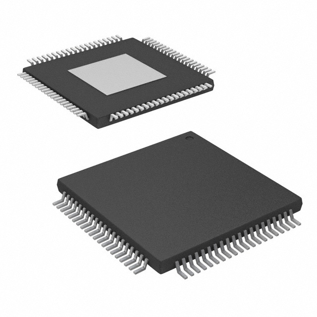
eTQFP80
10 mm × 10 mm × 1.0 mm
0.4 mm pitch
eTQFP100
14 mm × 14 mm × 1.0 mm
0.5 mm pitch
Features
• Enhanced analog-to-digital converter system
with:
– Three 12-bit SAR analog converters
– One 16-bit Sigma-Delta analog converters
• Decimation unit to support SD ADC data
conditioning
• Two deserial serial peripheral interface (DSPI)
modules
• AEC-Q100 qualified
• One main 32-bit Power Architecture® VLE
Compliant CPU core, single issue
– Single-precision floating point operations
• 1568 KB on-chip RWW flash memory
– Supporting EEPROM emulation (32 KB)
• Two LIN and UART communication interfaces
(LINFlexD) modules
• One μs-bus channel (composed by one DSPI
and one LINFlexD)
• Four SENT channels
• 64 KB general-purpose data SRAM
• Two modular controller area network (M_CAN)
modules
• System Memory Protection Unit (SMPU)
• Fast Ethernet controller (FEC)
• Multi-channel direct memory access controllers
(eDMA) with 16-channel for up to 60 DMA
sources
• Interrupt controller (INTC)
• Four 32-bit and one 64-bit Periodic Interrupt
Timer channels (PIT)
• Single phase-locked loops with stable clock
domain for peripherals and core (PLL)
• System integration unit lite (SIUL2)
• Boot assist flash (BAF) supports factory
programming through UART/LIN, CAN
• Generic timer module (GTM101)
• Fast Asynchronous Serial Transmission
(LFAST)
• Nexus development interface (NDI) per IEEEISTO 5001-2003 standard, with some support
for 2010 standard
• Device and board test support per Joint Test
Action Group (JTAG) (IEEE 1149.1 and IEEE
1149.7)
• Single 5 V +/-10% Power supply supporting
cold start conditions (down to 3.0 V)
• Self Test capability
• Designed for eTQFP80 and eTQFP100
Table 1. Device summary
Root Part Numbers
Memory Flash size
Package eTQFP80
Package eTQFP100
1056 KByte
SPC572L60F2
SPC572L60E3
1568 KByte
SPC572L64F2
SPC572L64E3
July 2017
This is information on a product in full production.
DocID027866 Rev 5
1/112
www.st.com
�Table of contents
SPC572Lx
Table of contents
1
2
3
2/112
Introduction . . . . . . . . . . . . . . . . . . . . . . . . . . . . . . . . . . . . . . . . . . . . . . . . 7
1.1
Document overview . . . . . . . . . . . . . . . . . . . . . . . . . . . . . . . . . . . . . . . . . . 7
1.2
Description . . . . . . . . . . . . . . . . . . . . . . . . . . . . . . . . . . . . . . . . . . . . . . . . . 7
1.3
Device feature summary . . . . . . . . . . . . . . . . . . . . . . . . . . . . . . . . . . . . . . 7
1.4
Block diagram . . . . . . . . . . . . . . . . . . . . . . . . . . . . . . . . . . . . . . . . . . . . . . . 8
1.5
Features overview . . . . . . . . . . . . . . . . . . . . . . . . . . . . . . . . . . . . . . . . . . .11
Package pinouts and signal descriptions . . . . . . . . . . . . . . . . . . . . . . . 13
2.1
Package pinouts . . . . . . . . . . . . . . . . . . . . . . . . . . . . . . . . . . . . . . . . . . . . 13
2.2
Pin descriptions . . . . . . . . . . . . . . . . . . . . . . . . . . . . . . . . . . . . . . . . . . . . 14
2.2.1
Power supply and reference voltage pins . . . . . . . . . . . . . . . . . . . . . . . 14
2.2.2
System pins . . . . . . . . . . . . . . . . . . . . . . . . . . . . . . . . . . . . . . . . . . . . . . 15
2.2.3
LVDS pins . . . . . . . . . . . . . . . . . . . . . . . . . . . . . . . . . . . . . . . . . . . . . . . 16
2.2.4
Generic pins . . . . . . . . . . . . . . . . . . . . . . . . . . . . . . . . . . . . . . . . . . . . . . 16
Electrical characteristics . . . . . . . . . . . . . . . . . . . . . . . . . . . . . . . . . . . . 18
3.1
Introduction . . . . . . . . . . . . . . . . . . . . . . . . . . . . . . . . . . . . . . . . . . . . . . . 18
3.2
Parameter classification . . . . . . . . . . . . . . . . . . . . . . . . . . . . . . . . . . . . . . 18
3.3
Absolute maximum ratings . . . . . . . . . . . . . . . . . . . . . . . . . . . . . . . . . . . . 19
3.4
Electromagnetic Compatibility (EMC) . . . . . . . . . . . . . . . . . . . . . . . . . . . . 20
3.5
Electrostatic discharge (ESD) . . . . . . . . . . . . . . . . . . . . . . . . . . . . . . . . . 20
3.6
Operating conditions . . . . . . . . . . . . . . . . . . . . . . . . . . . . . . . . . . . . . . . . 20
3.7
DC electrical specifications . . . . . . . . . . . . . . . . . . . . . . . . . . . . . . . . . . . 22
3.8
I/O pad specification . . . . . . . . . . . . . . . . . . . . . . . . . . . . . . . . . . . . . . . . . 23
3.8.1
I/O input DC characteristics . . . . . . . . . . . . . . . . . . . . . . . . . . . . . . . . . . 24
3.8.2
I/O output DC characteristics . . . . . . . . . . . . . . . . . . . . . . . . . . . . . . . . . 28
3.9
I/O pad current specification . . . . . . . . . . . . . . . . . . . . . . . . . . . . . . . . . . . 33
3.10
Reset pad (PORST, ESR0) electrical characteristics . . . . . . . . . . . . . . . . 36
3.11
Oscillator and PLL . . . . . . . . . . . . . . . . . . . . . . . . . . . . . . . . . . . . . . . . . . 39
3.12
ADC specifications . . . . . . . . . . . . . . . . . . . . . . . . . . . . . . . . . . . . . . . . . . 43
3.12.1
ADC input description . . . . . . . . . . . . . . . . . . . . . . . . . . . . . . . . . . . . . . 43
3.12.2
SAR ADC electrical specification . . . . . . . . . . . . . . . . . . . . . . . . . . . . . . 46
DocID027866 Rev 5
�SPC572Lx
Table of contents
3.12.3
3.13
Temperature sensor . . . . . . . . . . . . . . . . . . . . . . . . . . . . . . . . . . . . . . . . . 57
3.14
LVDS Fast Asynchronous Serial Transmission (LFAST) pad electrical
characteristics . . . . . . . . . . . . . . . . . . . . . . . . . . . . . . . . . . . . . . . . . . . . . 57
3.15
4
S/D ADC electrical specification . . . . . . . . . . . . . . . . . . . . . . . . . . . . . . 50
3.14.1
LFAST interface timing diagrams . . . . . . . . . . . . . . . . . . . . . . . . . . . . . . 58
3.14.2
LFAST and MSC/DSPI LVDS interface electrical characteristics . . . . . 59
Power management: PMC, POR/LVD, sequencing . . . . . . . . . . . . . . . . . 62
3.15.1
Power management integration . . . . . . . . . . . . . . . . . . . . . . . . . . . . . . . 63
3.15.2
Main voltage regulator electrical characteristics . . . . . . . . . . . . . . . . . . 63
3.15.3
Device voltage monitoring . . . . . . . . . . . . . . . . . . . . . . . . . . . . . . . . . . . 65
3.15.4
Power up/down sequencing . . . . . . . . . . . . . . . . . . . . . . . . . . . . . . . . . . 66
3.16
Flash memory electrical characteristics . . . . . . . . . . . . . . . . . . . . . . . . . . 67
3.17
AC specifications . . . . . . . . . . . . . . . . . . . . . . . . . . . . . . . . . . . . . . . . . . . 70
3.17.1
Debug and calibration interface timing . . . . . . . . . . . . . . . . . . . . . . . . . 70
3.17.2
DSPI timing with CMOS and LVDS pads . . . . . . . . . . . . . . . . . . . . . . . . 75
3.17.3
FEC timing . . . . . . . . . . . . . . . . . . . . . . . . . . . . . . . . . . . . . . . . . . . . . . . 87
3.17.4
UART timing . . . . . . . . . . . . . . . . . . . . . . . . . . . . . . . . . . . . . . . . . . . . . 90
3.17.5
GPIO delay timing . . . . . . . . . . . . . . . . . . . . . . . . . . . . . . . . . . . . . . . . . 90
Package characteristics . . . . . . . . . . . . . . . . . . . . . . . . . . . . . . . . . . . . . 91
4.1
ECOPACK®
4.2
eTQFP80 case drawing . . . . . . . . . . . . . . . . . . . . . . . . . . . . . . . . . . . . . . 92
4.3
eTQFP100 case drawing . . . . . . . . . . . . . . . . . . . . . . . . . . . . . . . . . . . . . 95
4.4
Thermal characteristics . . . . . . . . . . . . . . . . . . . . . . . . . . . . . . . . . . . . . . 97
4.4.1
. . . . . . . . . . . . . . . . . . . . . . . . . . . . . . . . . . . . . . . . . . . . . . . . . . . . . . . . . . . . 91
General notes for specifications at maximum junction temperature . . . 98
5
Ordering information . . . . . . . . . . . . . . . . . . . . . . . . . . . . . . . . . . . . . . 101
6
Revision history . . . . . . . . . . . . . . . . . . . . . . . . . . . . . . . . . . . . . . . . . . 102
DocID027866 Rev 5
3/112
3
�List of tables
SPC572Lx
List of tables
Table 1.
Table 2.
Table 3.
Table 4.
Table 5.
Table 6.
Table 7.
Table 8.
Table 9.
Table 10.
Table 11.
Table 12.
Table 13.
Table 14.
Table 15.
Table 16.
Table 17.
Table 18.
Table 19.
Table 20.
Table 21.
Table 22.
Table 23.
Table 24.
Table 25.
Table 26.
Table 27.
Table 28.
Table 29.
Table 30.
Table 31.
Table 32.
Table 33.
Table 34.
Table 35.
Table 36.
Table 37.
Table 38.
Table 39.
Table 40.
Table 41.
Table 42.
Table 43.
Table 44.
4/112
Device summary . . . . . . . . . . . . . . . . . . . . . . . . . . . . . . . . . . . . . . . . . . . . . . . . . . . . . . . . . . 1
SPC572Lx device feature summary . . . . . . . . . . . . . . . . . . . . . . . . . . . . . . . . . . . . . . . . . . . 7
Power supply and reference pins . . . . . . . . . . . . . . . . . . . . . . . . . . . . . . . . . . . . . . . . . . . . 15
System pins . . . . . . . . . . . . . . . . . . . . . . . . . . . . . . . . . . . . . . . . . . . . . . . . . . . . . . . . . . . . 15
LVDSM pin descriptions . . . . . . . . . . . . . . . . . . . . . . . . . . . . . . . . . . . . . . . . . . . . . . . . . . . 16
Parameter classifications . . . . . . . . . . . . . . . . . . . . . . . . . . . . . . . . . . . . . . . . . . . . . . . . . . 18
Absolute maximum ratings . . . . . . . . . . . . . . . . . . . . . . . . . . . . . . . . . . . . . . . . . . . . . . . . . 19
ESD ratings, . . . . . . . . . . . . . . . . . . . . . . . . . . . . . . . . . . . . . . . . . . . . . . . . . . . . . . . . . . . . 20
Device operating conditions . . . . . . . . . . . . . . . . . . . . . . . . . . . . . . . . . . . . . . . . . . . . . . . . 21
DC electrical specifications . . . . . . . . . . . . . . . . . . . . . . . . . . . . . . . . . . . . . . . . . . . . . . . . . 23
I/O pad specification descriptions . . . . . . . . . . . . . . . . . . . . . . . . . . . . . . . . . . . . . . . . . . . . 24
I/O input DC electrical characteristics . . . . . . . . . . . . . . . . . . . . . . . . . . . . . . . . . . . . . . . . . 25
I/O pull-up/pull-down DC electrical characteristics . . . . . . . . . . . . . . . . . . . . . . . . . . . . . . . 26
WEAK configuration output buffer electrical characteristics . . . . . . . . . . . . . . . . . . . . . . . . 29
MEDIUM configuration output buffer electrical characteristics . . . . . . . . . . . . . . . . . . . . . . 30
STRONG configuration output buffer electrical characteristics. . . . . . . . . . . . . . . . . . . . . . 31
VERY STRONG configuration output buffer electrical characteristics . . . . . . . . . . . . . . . . 32
I/O consumption . . . . . . . . . . . . . . . . . . . . . . . . . . . . . . . . . . . . . . . . . . . . . . . . . . . . . . . . . 34
Reset electrical characteristics . . . . . . . . . . . . . . . . . . . . . . . . . . . . . . . . . . . . . . . . . . . . . . 38
PLL0 electrical characteristics . . . . . . . . . . . . . . . . . . . . . . . . . . . . . . . . . . . . . . . . . . . . . . 40
External oscillator electrical specifications . . . . . . . . . . . . . . . . . . . . . . . . . . . . . . . . . . . . . 41
Selectable load capacitance . . . . . . . . . . . . . . . . . . . . . . . . . . . . . . . . . . . . . . . . . . . . . . . . 42
Internal RC oscillator electrical specifications. . . . . . . . . . . . . . . . . . . . . . . . . . . . . . . . . . . 43
ADC pin specification . . . . . . . . . . . . . . . . . . . . . . . . . . . . . . . . . . . . . . . . . . . . . . . . . . . . . 45
SARn ADC electrical specification . . . . . . . . . . . . . . . . . . . . . . . . . . . . . . . . . . . . . . . . . . . 47
SDn ADC electrical specification . . . . . . . . . . . . . . . . . . . . . . . . . . . . . . . . . . . . . . . . . . . . 50
Temperature sensor electrical characteristics . . . . . . . . . . . . . . . . . . . . . . . . . . . . . . . . . . 57
LVDS pad startup and receiver electrical characteristics . . . . . . . . . . . . . . . . . . . . . . . . . . 59
LFAST transmitter electrical characteristics . . . . . . . . . . . . . . . . . . . . . . . . . . . . . . . . . . . . 61
MSC/DSPI LVDS transmitter electrical characteristics . . . . . . . . . . . . . . . . . . . . . . . . . . . 61
Voltage regulator electrical characteristics . . . . . . . . . . . . . . . . . . . . . . . . . . . . . . . . . . . . . 64
Voltage monitor electrical characteristics . . . . . . . . . . . . . . . . . . . . . . . . . . . . . . . . . . . . . . 65
Device supply relation during power-up/power-down sequence. . . . . . . . . . . . . . . . . . . . . 66
Functional terminals state during power-up and reset . . . . . . . . . . . . . . . . . . . . . . . . . . . . 66
RWSC settings . . . . . . . . . . . . . . . . . . . . . . . . . . . . . . . . . . . . . . . . . . . . . . . . . . . . . . . . . . 67
Flash memory program and erase specifications (pending silicon characterization) . . . . . 68
Flash memory module extended life specification . . . . . . . . . . . . . . . . . . . . . . . . . . . . . . . 69
JTAG pin AC electrical characteristics . . . . . . . . . . . . . . . . . . . . . . . . . . . . . . . . . . . . . . . . 70
Nexus debug port timing . . . . . . . . . . . . . . . . . . . . . . . . . . . . . . . . . . . . . . . . . . . . . . . . . . . 73
DSPI channel frequency support . . . . . . . . . . . . . . . . . . . . . . . . . . . . . . . . . . . . . . . . . . . . 75
DSPI CMOS master classic timing (full duplex and output only) – MTFE = 0, CPHA = 0 or 1
.............................................................................................................................................76
DSPI CMOS master modified timing (full duplex and output only) – MTFE = 1, CPHA = 0 or
1 . . . . . . . . . . . . . . . . . . . . . . . . . . . . . . . . . . . . . . . . . . . . . . . . . . . . . . . . . . . . . . . . . . . . . 79
DSPI LVDS master timing – output only – timed serial bus mode TSB = 1 or ITSB = 1,
CPOL = 0 or 1, continuous SCK clock . . . . . . . . . . . . . . . . . . . . . . . . . . . . . . . . . . . . . . . . 83
DSPI CMOS master timing – output only – timed serial bus mode TSB = 1 or ITSB = 1,
CPOL = 0 or 1, continuous SCK clock . . . . . . . . . . . . . . . . . . . . . . . . . . . . . . . . . . . . . . . . 84
DocID027866 Rev 5
�SPC572Lx
Table 45.
Table 46.
Table 47.
Table 48.
Table 49.
Table 50.
Table 51.
Table 52.
Table 53.
Table 54.
Table 55.
List of tables
DSPI CMOS Slave timing - Modified Transfer Format (MTFE = 0/1) . . . . . . . . . . . . . . . . . 85
RMII serial management channel timing . . . . . . . . . . . . . . . . . . . . . . . . . . . . . . . . . . . . . . 87
RMII receive signal timing. . . . . . . . . . . . . . . . . . . . . . . . . . . . . . . . . . . . . . . . . . . . . . . . . . 88
RMII transmit signal timing . . . . . . . . . . . . . . . . . . . . . . . . . . . . . . . . . . . . . . . . . . . . . . . . . 89
UART frequency support . . . . . . . . . . . . . . . . . . . . . . . . . . . . . . . . . . . . . . . . . . . . . . . . . . 90
GPIO delay timing. . . . . . . . . . . . . . . . . . . . . . . . . . . . . . . . . . . . . . . . . . . . . . . . . . . . . . . . 90
eTQFP80 – STMicroelectronics package mechanical data . . . . . . . . . . . . . . . . . . . . . . . . 93
eTQFP100 – STMicroelectronics package mechanical data . . . . . . . . . . . . . . . . . . . . . . . 96
Thermal characteristics for eTQFP80 . . . . . . . . . . . . . . . . . . . . . . . . . . . . . . . . . . . . . . . . . 97
Thermal characteristics for eTQFP100 . . . . . . . . . . . . . . . . . . . . . . . . . . . . . . . . . . . . . . . . 98
Document revision history . . . . . . . . . . . . . . . . . . . . . . . . . . . . . . . . . . . . . . . . . . . . . . . . 102
DocID027866 Rev 5
5/112
5
�List of figures
SPC572Lx
List of figures
Figure 1.
Figure 2.
Figure 3.
Figure 4.
Figure 5.
Figure 6.
Figure 7.
Figure 8.
Figure 9.
Figure 10.
Figure 11.
Figure 12.
Figure 13.
Figure 14.
Figure 15.
Figure 16.
Figure 17.
Figure 18.
Figure 19.
Figure 20.
Figure 21.
Figure 22.
Figure 23.
Figure 24.
Figure 25.
Figure 26.
Figure 27.
Figure 28.
Figure 29.
Figure 30.
Figure 31.
Figure 32.
Figure 33.
Figure 34.
Figure 35.
Figure 36.
Figure 37.
Figure 38.
Figure 39.
Figure 40.
6/112
Block diagram . . . . . . . . . . . . . . . . . . . . . . . . . . . . . . . . . . . . . . . . . . . . . . . . . . . . . . . . . . . . 9
Periphery allocation . . . . . . . . . . . . . . . . . . . . . . . . . . . . . . . . . . . . . . . . . . . . . . . . . . . . . . 10
80-pin QFP configuration (top view) . . . . . . . . . . . . . . . . . . . . . . . . . . . . . . . . . . . . . . . . . . 13
100-pin QFP configuration (top view) . . . . . . . . . . . . . . . . . . . . . . . . . . . . . . . . . . . . . . . . . 14
I/O input DC electrical characteristics definition . . . . . . . . . . . . . . . . . . . . . . . . . . . . . . . . . 24
Weak pull-up electrical characteristics definition . . . . . . . . . . . . . . . . . . . . . . . . . . . . . . . . 27
I/O output DC electrical characteristics definition . . . . . . . . . . . . . . . . . . . . . . . . . . . . . . . . 28
Start-up reset requirements . . . . . . . . . . . . . . . . . . . . . . . . . . . . . . . . . . . . . . . . . . . . . . . . 37
Noise filtering on reset signal . . . . . . . . . . . . . . . . . . . . . . . . . . . . . . . . . . . . . . . . . . . . . . . 38
PLL integration . . . . . . . . . . . . . . . . . . . . . . . . . . . . . . . . . . . . . . . . . . . . . . . . . . . . . . . . . . 40
Test circuit . . . . . . . . . . . . . . . . . . . . . . . . . . . . . . . . . . . . . . . . . . . . . . . . . . . . . . . . . . . . . 43
Input equivalent circuit (Fast SARn channels) . . . . . . . . . . . . . . . . . . . . . . . . . . . . . . . . . . 44
Input equivalent circuit (SARB channels) . . . . . . . . . . . . . . . . . . . . . . . . . . . . . . . . . . . . . . 45
LFAST and MSC/DSPI LVDS timing definition . . . . . . . . . . . . . . . . . . . . . . . . . . . . . . . . . . 58
Power-down exit time . . . . . . . . . . . . . . . . . . . . . . . . . . . . . . . . . . . . . . . . . . . . . . . . . . . . . 59
Rise/fall time . . . . . . . . . . . . . . . . . . . . . . . . . . . . . . . . . . . . . . . . . . . . . . . . . . . . . . . . . . . . 59
LVDS pad external load diagram . . . . . . . . . . . . . . . . . . . . . . . . . . . . . . . . . . . . . . . . . . . . 62
Voltage regulator capacitance connection . . . . . . . . . . . . . . . . . . . . . . . . . . . . . . . . . . . . . 63
Voltage monitor threshold definition . . . . . . . . . . . . . . . . . . . . . . . . . . . . . . . . . . . . . . . . . . 65
JTAG test clock input timing . . . . . . . . . . . . . . . . . . . . . . . . . . . . . . . . . . . . . . . . . . . . . . . . 71
JTAG test access port timing . . . . . . . . . . . . . . . . . . . . . . . . . . . . . . . . . . . . . . . . . . . . . . . 71
JTAG JCOMP timing . . . . . . . . . . . . . . . . . . . . . . . . . . . . . . . . . . . . . . . . . . . . . . . . . . . . . 72
JTAG boundary scan timing . . . . . . . . . . . . . . . . . . . . . . . . . . . . . . . . . . . . . . . . . . . . . . . . 73
Nexus event trigger and test clock timings . . . . . . . . . . . . . . . . . . . . . . . . . . . . . . . . . . . . . 74
Nexus TDI/TDIC, TMS/TMSC, TDO/TDOC timing . . . . . . . . . . . . . . . . . . . . . . . . . . . . . . . 75
DSPI CMOS master mode – classic timing, CPHA = 0 . . . . . . . . . . . . . . . . . . . . . . . . . . . 78
DSPI CMOS master mode – classic timing, CPHA = 1 . . . . . . . . . . . . . . . . . . . . . . . . . . . 78
DSPI PCS strobe (PCSS) timing (master mode) . . . . . . . . . . . . . . . . . . . . . . . . . . . . . . . . 79
DSPI CMOS master mode – modified timing, CPHA = 0 . . . . . . . . . . . . . . . . . . . . . . . . . . 82
DSPI CMOS master mode – modified timing, CPHA = 1 . . . . . . . . . . . . . . . . . . . . . . . . . . 82
DSPI PCS strobe (PCSS) timing (master mode) . . . . . . . . . . . . . . . . . . . . . . . . . . . . . . . . 83
DSPI LVDS and CMOS master timing – output only – modified transfer format MTFE = 1,
CHPA = 1 . . . . . . . . . . . . . . . . . . . . . . . . . . . . . . . . . . . . . . . . . . . . . . . . . . . . . . . . . . . . . . 85
DSPI Slave Mode - Modified transfer format timing (MFTE = 0/1) — CPHA = 0 . . . . . . . . 86
DSPI Slave Mode - Modified transfer format timing (MFTE = 0/1) — CPHA = 1 . . . . . . . . 87
RMII serial management channel timing diagram. . . . . . . . . . . . . . . . . . . . . . . . . . . . . . . . 88
RMII receive signal timing diagram. . . . . . . . . . . . . . . . . . . . . . . . . . . . . . . . . . . . . . . . . . . 89
RMII transmit signal timing diagram . . . . . . . . . . . . . . . . . . . . . . . . . . . . . . . . . . . . . . . . . . 89
eTQFP80 – STMicroelectronics package mechanical drawing . . . . . . . . . . . . . . . . . . . . . 92
eTQFP100 – STMicroelectronics package mechanical drawing . . . . . . . . . . . . . . . . . . . . 95
Product code structure . . . . . . . . . . . . . . . . . . . . . . . . . . . . . . . . . . . . . . . . . . . . . . . . . . . 101
DocID027866 Rev 5
�SPC572Lx
Introduction
1
Introduction
1.1
Document overview
This document provides electrical specifications, pin assignments, and package diagrams for
the SPC572Lx series of microcontroller units (MCUs). For functional characteristics, see the
device reference manual.
1.2
Description
This family of MCUs is targeted at automotive powertrain controller applications for fourcylinder gasoline and diesel engines, chassis control applications, transmission control
applications, steering and braking applications, as well as low-end hybrid applications.
The family is designed to achieve ISO26262 ASIL-A compliance.
1.3
Device feature summary
Table 2. SPC572Lx device feature summary
Feature
Description
Process
Main processor
55 nm
Core
e200z2
Number of main cores
1
Single precision floating point
Yes
VLE
Yes
Main processor frequency
80 MHz
SMPU
Yes
Software watchdog timer (task SWT/safety SWT)
Core Nexus class
2 (1/1)
3
Sequence processing unit (SPU)
Yes
System SRAM
64 KB
Flash memory
1536 KB
Flash memory fetch accelerator
8 × 128 bit
Data flash memory (EEPROM)
2 × 16 KB
Flash memory overlay RAM
8 KB
DMA channels
16
LINFlexD (UART/MSC)
3 (2/1)
M_CAN/M_TTCAN
2/0
DSPI (SPI/MSC/sync SCI)
2 (1/1/0)
Microsecond bus downlink
Yes
DocID027866 Rev 5
7/112
111
�Introduction
SPC572Lx
Table 2. SPC572Lx device feature summary (continued)
Feature
Description
SENT bus
4 channels
Ethernet
Yes
Zipwire (SIPI / LFAST) Interprocessor bus
High speed (4-phase only)
System timers
4 PIT channels
1 AUTOSAR® (STM)
64-bit PIT
GTM timer
16 input channels,
56 output channels
GTM RAM
18.53 KB
Interrupt controller
1024 sources
ADC (SAR)
3
ADC (SD)
1
Temperature sensor
Yes
PLL
Single PLL with no FM
Internal linear voltage regulator
1.2 V
5 V(1)
3.3 V(2)
External power supplies
Low-power modes
Stop mode
Slow mode
Packages
eTQFP80
eTQFP100
1. The device can be powered up at 5 V only.
2. Optional: can be used for special I/O segments
1.4
Block diagram
Figure 1 and Figure 2 show the top-level block diagrams.
8/112
DocID027866 Rev 5
�SPC572Lx
Introduction
Figure 1. Block diagram
DCI (without
LFAST support)
SPU
JTAGM
SWT_3
DMA CH MUX
SWT_2
Zipwire
(LFAST
& SIPI)
Ethernet
INTC_2
16ch eDMA
40 MHz
Scalar SP-FPU
Concentrator
40 MHz
BIU
Load/Store
32 ADD
32 DATA
32 ADD
32 DATA
M2
32 ADD
32 DATA
Peripheral Bridge
40 MHz
Decorated Storage
32 ADD
32 DATA
Peripheral Cluster
(see Periphery
allocation diagram)
STM_2
e200z215An3–80 MHz
Core
Nexus 3
VLE
S2
JTAGC
Cross Bar Switch (AMBA 2.0 v6 AHB)–80 MHz
System Memory Protection Unit (SMPU)
S1
32 ADD
32 DATA
SRAM Control
Decorated Access
32 ADD
32 DATA
SRAM
64 KB
Instruction
32 ADD
32 DATA
M1
M0
S0
32 ADD
32 DATA
Overlay Backdoor
for system RAM
Flash Controller
8 x 128 Mini Cache
NAR
128-bit Page Line
1.5 MB flash
6 x 256 KB code flash
RAM 8 KB
Overlay/Trace
DocID027866 Rev 5
2 x 16 KB data EEPROM
NVM
9/112
111
�Introduction
SPC572Lx
Figure 2. Periphery allocation
SSCM
PASS
Flash control
LFAST_0
SIPI_0
SIUL2
MC_ME
MC_CGM
CMU_PLL
PLLDIG
XOSC
IRCOSC
MC_RGM
PMCDIG
MC_PCU
WKPU
DECIFILTER
PBRIDGE_A
XBAR_0
SMPU_0
PRAM_0
PCM
PFLASH_0
INTC_0
SWT_2
SWT_3
STM_2
DMA_0
FEC_0
EIM
ERM
GTM
SAR ADC_0
SAR ADC_4
SAR ADC_B
PIT_0
PIT_1
JTAGM
DMAMUX
SD ADC_3
DTS
JDC
SENT SRX_0
DSPI_0
DSPI_4
LINFlexD_0
LINFlexD_1
LINFlexD_14
CAN SRAM
CCCU
M_CAN_1
M_CAN_2
Peripheral Bus A
Peripheral Cluster A
10/112
DocID027866 Rev 5
�SPC572Lx
1.5
Introduction
Features overview
On-chip modules within SPC572Lx include the following features:
•
•
1 main CPU, single issue, 32-bit CPU core complex (e200z2)
–
Power Architecture embedded specification compliance
–
Instruction set enhancement allowing variable length encoding (VLE), encoding a
mix of 16-bit and 32-bit instructions, for code size footprint reduction
–
Single-precision floating point operations
–
Saturation Instructions Extension adding scalar saturating arithmetic support to
the PowerISA Integer Saturation (ISAT)
1568 KB (1536 KB code flash + 32 KB data flash) on-chip flash memory
–
Supporting multiple blocks allowing EEPROM emulation
–
RWW between data EEPROM and code flash memory
•
64 KB general-purpose data SRAM
•
System Memory Protection Unit (SMPU)
•
16-channel Direct Memory Access controllers (eDMA) with two channel multiplexers for
up to 60 DMA sources
•
Interrupt Controller (INTC) supporting up to 1024 interrupt sources (all are not
assigned)
•
System Timer Module (STM)
•
2 Software Watchdog Timers (SWT)
•
2 Periodic Interrupt Timers (PIT)
–
1 PIT with four standard 32-bit timer channels
–
1 PIT with two 32-bit timer channels which can be combined into one 64-bit
channel
•
Single phase-locked loop with stable clock domain for peripherals and core (PLL)
•
Single crossbar switch architecture for concurrent access to peripherals, flash memory,
or SRAM from multiple bus masters
•
System Integration Unit Lite (SIUL2)
•
Boot Assist Flash (BAF) supports factory programming using a serial bootload through
the UART Serial Boot Mode Protocol (physical interface (PHY) can be e.g., UART and
CAN)
•
PASS module (supporting 256-bit JTAG password protection)
•
Device life cycle monitoring
•
Generic Timer Module (GTM101)
•
Enhanced analog-to-digital converter system with:
–
Three 12-bit SAR analog converters
–
One 16-bit Sigma-Delta analog converter
•
Decimation unit to support SD ADC data conditioning
•
1 Deserial Serial Peripheral Interface (DSPI) module
•
2 LIN and UART communication interfaces (LINFlexD) modules
•
1 microsecond-bus channel (composed of one DSPI and one LINFlexD)
•
4 SENT (Single Edge Nibble Transmission) channels
•
2 Modular Controller Area Network (M_CAN) modules
DocID027866 Rev 5
11/112
111
�Introduction
12/112
SPC572Lx
•
1 Clock Calibration on CAN Unit (CCCU)
•
Fast Ethernet Controller (FEC)
•
Fast Asynchronous Serial Transmission (LFAST)
•
Nexus Development Interface (NDI) per IEEE-ISTO 5001-2003 standard, with partial
support for 2010 standard
•
Device and board test support per Joint Test Action Group (JTAG) (IEEE 1149.1 and
IEEE 1149.7)
•
On-chip voltage regulator controller manages the supply voltage down to 1.2 V for core
logic
•
Self-test capability
DocID027866 Rev 5
�SPC572Lx
Package pinouts and signal descriptions
2
Package pinouts and signal descriptions
2.1
Package pinouts
The QFP package pinouts are shown in Figure 3 and Figure 4.
VDD_HV_IO_MAIN
PA[11]
PA[10]
PA[13]
PA[12]
PA[1]
PA[2]
67
66
65
64
63
62
61
PD[3]
VDD_HV_IO_FLA
PD[2]
68
PD[1]
70
69
PD[0]
71
PE[12]
72
73
PC[13]
76
PC[14]
VDD_HV_IO_ETH
77
PC[15]
PC[12]
78
74
PC[11]
79
75
PC[10]
80
Figure 3. 80-pin QFP configuration (top view)
eTQFP80
46
PF[13]
VDD_HV_IO_MAIN
16
45
PB[15]
17
44
VDD_HV_IO_JTAG/
VDD_HV_OSC
XTAL
PB[14]
18
43
EXTAL
PB[13]
19
42
VDD_LV
PB[12]
20
41
VDD_HV_IO_MAIN
DocID027866 Rev 5
40
15
PA[15]
PD[7]
VDD_LV
39
47
PD[8]
14
38
PD[6]
PE[1]
PA[3]
48
37
13
36
PA[8]
PE[0]
PB[8]
49
PB[9]
12
35
PA[7]
PC[0]
34
50
PB[11]
11
PB[10]
PA[9]
PC[1]
33
51
VDD_HV_ADV
PA[5]
10
32
52
PC[2]
PB[0]
9
31
PA[6]
PC[3]
PB[1]
8
53
30
TESTMODE
PC[4]
PB[2]
54
29
7
28
VDD_HV_PMC
PC[5]
PB[3]
55
PD[11]
6
27
PORST
PC[6]
PE[13]
56
26
5
PB[4]
ESR0
PC[7]
25
57
PE[14]
4
24
PD[4]
PC[8]
VDD_HV_ADR
58
23
3
VSS_HV_ADR
PD[5]
PC[9]
22
PE[9]
59
21
60
2
PG[8]
1
PD[15]
PG[7]
PD[14]
13/112
111
�Package pinouts and signal descriptions
SPC572Lx
PC[14]
PC[15]
PE[12]
PD[0]
PD[1]
PD[2]
PD[3]
VDD_HV_IO_FLA
VDD_HV_IO_MAIN
PE[11]
PE[10]
PA[11]
PA[10]
PA[0]
93
92
91
90
89
88
87
86
85
84
83
82
81
80
PA[2]
PC[13]
94
PA[1]
VDD_HV_IO_ETH
95
PA[12]
PC[12]
96
77
76
PC[11]
97
PA[13]
PC[10]
98
78
PF[3]
99
79
PF[2]
100
Figure 4. 100-pin QFP configuration (top view)
75
PE[9]
74
PE[8]
3
73
PD[5]
PC[8]
4
72
PD[4]
PC[7]
5
71
PE[7]
PC[6]
6
70
PE[6]
PC[5]
7
69
PE[5]
PC[4]
8
68
VDD_LV
PC[3]
9
67
ESR0
PC[2]
10
66
PORST
PC[1]
11
65
ESR1
PC[0]
12
64
TESTMODE
PE[0]
13
63
PA[6]
PE[1]
14
62
PA[5]
PE[2]
15
61
PA[9]
PD[12]
16
60
PA[7]
PD[13]
17
59
PA[8]
PE[3]
18
58
PD[6]
VDD_LV
19
57
PD[7]
VDD_HV_IO_MAIN
20
56
PF[13]
PB[15]
21
55
PB[14]
22
54
PB[13]
23
53
VDD_HV_IO_JTAG/
VDD_HV_OSC
XTAL
EXTAL
PB[12]
24
52
VDD_LV
PG[6]
25
51
VDD_HV_IO_MAIN
2.2
41
42
43
44
45
46
47
48
49
PF[0]
PD[9]
PD[10]
PB[11]
PB[10]
PB[9]
PB[8]
PA[3]
PD[8]
PA[15]
50
40
PB[3]
PF[1]
35
PD[11]
39
34
PE[13]
VDD_HV_ADV
33
PB[4]
38
32
PE[14]
PB[0]
31
37
30
PE[15]
PB[1]
29
VDD_HV_ADR
36
28
VSS_HV_ADR
PB[2]
27
PC[9]
eTQFP100
26
2
PG[8]
1
PD[15]
PG[7]
PD[14]
Pin descriptions
The following sections provide signal descriptions and related information about device
functionality and configuration.
2.2.1
Power supply and reference voltage pins
Table 3 contains information on power supply and reference pin functions for the devices.
See the Signal Table (Excel file) attached to this document. Locate the paperclip symbol on
the left side of the PDF window, and click it. Double-click on the excel file to open it and select
the Supply Pins Table tab.
14/112
DocID027866 Rev 5
�SPC572Lx
Package pinouts and signal descriptions
Table 3. Power supply and reference pins
Supply
Symbol
Type
QFP pin
Description
80
100
VSS_HV
Ground
High voltage ground
Exposed
pad 81
Exposed
pad 101
VSS_LV
Ground
Low voltage ground
Exposed
pad 81
Exposed
pad 101
VSS_HV_OSC
Ground
Ground supply for the oscillator
Exposed
pad 81
Exposed
pad 101
VDD_LV
Power
Low voltage power supply for
production device
(PLL is also powered by this pin.)
15, 42, 68
19, 52, 68
VDD_HV_PMC
Power
High voltage power supply for
internal power management unit
55
—
VDD_HV_IO_MAIN
Power
High voltage power supply for I/O
16, 41, 67
20, 51, 85
VDD_HV_IO_JTAG
Power
JTAG/Oscillator power supply
45
55
VDD_HV_OSC
Power
Oscillator voltage supply
45
55
VDD_HV_IO_ETH
Power
Ethernet 3.3 V I/O supply
77
95
VDD_HV_FLA
Power
Decoupling supply pin for flash
68
86
VDD_HV_ADV
Power
High voltage supply for ADC
33
39
VSS_HV_ADR
Reference
Ground reference of ADCs
23
28
VDD_HV_ADR
Reference
Voltage reference of ADCs
24
29
2.2.2
System pins
Table 4 contains information on system pin functions for the devices.
Table 4. System pins
QFP pin
Symbol
Description
Direction
80
100
PORST
Power on reset with Schmitt trigger characteristics and Bidirectional
noise filter. PORST is active low
56
66
ESR0
External functional reset with Schmitt trigger
characteristics and noise filter. ESR0 is active low
Bidirectional
57
67
Input only
54
64
TESTMODE Pin for testing purpose only.
An internal pull-down is implemented on the
TESTMODE pin to prevent the device from entering
TESTMODE. It is recommended to connect the
TESTMODE pin to VSS_HV_IO on the board. The value
of the TESTMODE pin is latched at the negation of
reset and has no affect afterward. The device will not
exit reset with the TESTMODE pin asserted during
power-up.
DocID027866 Rev 5
15/112
111
�Package pinouts and signal descriptions
SPC572Lx
Table 4. System pins (continued)
QFP pin
Symbol
Description
XTAL
Analog output of the oscillator amplifier circuit
needs to be grounded if oscillator is used in bypass
mode.
EXTAL
Analog input of the oscillator amplifier circuit when
oscillator is not in bypass mode
Analog input for the clock generator when oscillator is
in bypass mode
2.2.3
Direction
80
100
Output
44
54
Input
43
53
LVDS pins
Table 5 contains information on LVDS pin functions for the devices.
Table 5. LVDSM pin descriptions
Package pin number
Functional
block
SIPI
LFAST(1)
DSPI 4
Microsecond
Bus
Port
pin
Signal
PF[13]
SIPI_RXN
Interprocessor Bus LFAST,
LVDS Receive Negative
Terminal
PD[7]
SIPI_RXP
PD[6]
Signal description
Direction
eTQFP80
eTQFP100
I
46
56
Interprocessor Bus LFAST,
LVDS Receive Positive Terminal
I
47
57
SIPI_TXN
Interprocessor Bus LFAST,
LVDS Transmit Negative
Terminal
O
48
58
PA[8]
SIPI_TXP
Interprocessor Bus LFAST,
LVDS Transmit Positive
Terminal
O
49
59
PD[3]
SCK_N
DSPI 4 Microsecond Bus Serial
Clock, LVDS Negative Terminal
O
69
87
PD[2]
SCK_P
DSPI 4 Microsecond Bus Serial
Clock, LVDS Positive Terminal
O
70
88
PD[1]
SOUT_N
DSPI 4 Microsecond Bus Serial
Data, LVDS Negative Terminal
O
71
89
PD[0]
SOUT_P
DSPI 4 Microsecond Bus Serial
Data, LVDS Positive Terminal
O
72
90
1. DRCLK and TCK/DRCLK usage for SIPI LFAST is described in the SPC572Lx reference manual, refer to SIPI LFAST
chapter.
2.2.4
Generic pins
The I/O Signal Description Table contains information on generic pins. See the I/O Signal
Description and Input Multiplexing Tables (Excel file) attached to this document. Locate the
16/112
DocID027866 Rev 5
�SPC572Lx
Package pinouts and signal descriptions
paperclip symbol on the left side of the PDF window, and click it. Double-click on the excel
file to open it and select the I/O Signal Description Table tab.
DocID027866 Rev 5
17/112
111
�Electrical characteristics
SPC572Lx
3
Electrical characteristics
3.1
Introduction
This section contains detailed information on power considerations, DC/AC electrical
characteristics, and AC timing specifications.
In the tables where the device logic provides signals with their respective timing
characteristics, the symbol “CC” (Controller Characteristics) is included in the “Symbol”
column.
In the tables where the external system must provide signals with their respective timing
characteristics to the device, the symbol “SR” (System Requirement) is included in the
“Symbol” column.
Note:
Within this document, VDD_HV_IO refers to supply pins VDD_HV_IO_MAIN, VDD_HV_IO_JTAG,
VDD_HV_IO_ETH, VDD_HV_PMC and VDD_HV_FLA.
3.2
Parameter classification
The electrical parameters shown in this supplement are guaranteed by various methods. To
give the customer a better understanding, the classifications listed in Table 6 are used and
the parameters are tagged accordingly in the tables where appropriate.
Table 6. Parameter classifications
Classification tag
Note:
18/112
Tag description
P
Parameters are guaranteed by production testing on each individual device.
C
Parameters are guaranteed by the design characterization by measuring a statistically relevant
sample size across process variations.
T
Parameters are guaranteed by design characterization on a small sample size from typical
devices under typical conditions unless otherwise noted. All values shown in the typical column
are within this category.
D
Parameters are derived mainly from simulations.
The classification is shown in the column labeled “C” in the parameter tables where
appropriate.
DocID027866 Rev 5
�SPC572Lx
3.3
Electrical characteristics
Absolute maximum ratings
Table 7 describes the maximum ratings of the device.
Table 7. Absolute maximum ratings(1)
Value
Symbol
Parameter
Conditions
Unit
Min
Max
—
—
1000
k
—
—
—
—
—
–0.3
1.5
V
—
–0.3
6.0
V
SR SAR and S/D ADC supply voltage Reference to VSS_HV_ADV
–0.3
6.0
V
VSS_HV_ADR
SR SAR and S/D ADC low reference
–0.3
0.3
V
VDD_HV_ADR
SR SAR and S/D ADC high reference Reference to
–0.3
corresponding VSS_HV_ADR
6.0
V
SR I/O input voltage range(8)
–0.3
6.0
V
Relative to VSS_HV_IO
–0.3
—
Relative to VDD_HV_IO
—
0.3
Cycle
SR Lifetime power cycles
SR Ground voltage
VSS_HV
SR 1.2 V core supply voltage
VDD_LV
VDD_HV_IO(5)
VDD_HV_ADV
(7)
VIN
SR I/O supply voltage
(2),(3),(4)
(6)
Reference to VSS_HV
—
IINJD
SR Maximum DC injection current for Per pin, applies to all digital
digital pad
pins
–5
5
mA
IINJA
SR Maximum DC injection current for Per pin, applies to all
analog pad
analog pins
–5
5
mA
IMAXD
SR Maximum output DC current when Medium
driven
Strong
−7
8
mA
–10
10
–11
11
Very strong
SR Maximum current per power
segment(9)
—
–90
90
mA
SR Storage temperature range and
non-operating times
—
–55
175
°C
SR Maximum storage time, assembled No supply; storage
part programmed in ECU
temperature in range –40
°C to 60 °C
—
20
years
TSDR
SR Maximum solder temperature(10)
Pb-free package
—
—
260
°C
MSL
SR Moisture sensitivity level(11)
—
—
3
—
—
200
ms
IMAXSEG
TSTG
STORAGE
tXRAY
T
X-ray screen time
At 80÷130 KV; 20÷50 µA;
max 1 Gy dose
1. Functional operating conditions are given in the DC electrical specifications. Absolute maximum ratings are stress ratings
only, and functional operation at the maxima is not guaranteed. Stress beyond the listed maxima may affect device
reliability or cause permanent damage to the device.
2. Allowed 1.45 – 1.5 V for 60 seconds cumulative time at maximum TJ = 150 °C, remaining time as defined in note 5.
3. Allowed 1.375 – 1.45 V for 10 hours cumulative time at maximum TJ = 125 °C, remaining time as defined in note 5.
DocID027866 Rev 5
19/112
111
�Electrical characteristics
SPC572Lx
4. 1.32 – 1.375 V range allowed periodically for supply with sinusoidal shape and average supply value below 1.288 V at
maximum TJ = 125 °C
5. VDD_HV_IO refers to supply pins VDD_HV_IO_MAIN, VDD_HV_IO_JTAG, VDD_HV_IO_ETH, VDD_HV_OSC, VDD_HV_FLA.
6. Allowed 5.5–6.0 V for 60 seconds cumulative time with no restrictions, for 10 hours cumulative time device in reset, TJ
= 150 °C remaining time at or below 5.5 V.
7. VDD_HV_ADV is also the supply for the device temperature sensor and bandgap reference.
8. The maximum input voltage on an I/O pin tracks with the associated I/O supply maximum. For the injection current
condition on a pin, the voltage equals the supply plus the voltage drop across the internal ESD diode from I/O pin to supply.
The diode voltage varies significantly across process and temperature, but a value of 0.3 V can be used for nominal
calculations.
9. Sum of all controller pins (including both digital and analog) must not exceed 150 mA. A VDD_HV_IO power segment is
defined as one or more GPIO pins located between two VDD_HV_IO supply pins.
10. Solder profile per IPC/JEDEC J-STD-020D.
11. Moisture sensitivity per JEDEC test method A112.
3.4
Electromagnetic Compatibility (EMC)
EMC measurements to IC-level IEC standards are available from STMicroelectronics on
request.
3.5
Electrostatic discharge (ESD)
The following table describes the ESD ratings of the device.
Table 8. ESD ratings(1),(2)
Parameter
C
Conditions
Value
Unit
ESD for Human Body Model (HBM)(3)
T
All pins
2000
V
ESD for field induced Charged Device Model (CDM)(4)
T
All pins
500
V
1. All ESD testing is in conformity with CDF-AEC-Q100 Stress Test Qualification for Automotive Grade Integrated Circuits.
2. Device failure is defined as: “If after exposure to ESD pulses, the device does not meet the device specification
requirements, which includes the complete DC parametric and functional testing at room temperature and hot temperature.
Maximum DC parametrics variation within 10% of maximum specification”.
3. This parameter tested in conformity with ANSI/ESD STM5.1-2007 Electrostatic Discharge Sensitivity Testing.
4. This parameter tested in conformity with ANSI/ESD STM5.3-1990 Charged Device Model - Component Level.
3.6
Operating conditions
The following table describes the operating conditions for the device for which all
specifications in the datasheet are valid, except where explicitly noted.
The device operating conditions must not be exceeded or the functionality of the device is not
guaranteed.
20/112
DocID027866 Rev 5
�SPC572Lx
Electrical characteristics
Table 9. Device operating conditions(1)
Value
Symbol
C
Parameter
Conditions
Unit
Min
Typ
Max
—
—
80
MHz
Frequency
fSYS
CC
TJ −40 °C to 150 °C
C Device operating
frequency(2)
Temperature
TJ
SR
P Operating
temperature range junction
—
–40.0
—
150.0
°C
TA (TL to TH)
SR
P Ambient operating
temperature range
—
–40.0
—
125.0
°C
Voltage
VDD_LV
CC
VDD_HV_IO_MAIN(5) SR
P Core supply voltage
measured at external
pin(3)(4)
P I/O supply voltage
LVD400 enabled(6)
4.5
—
5.5
C
LVD400 disabled (6),
4.0
—
5.9
3.0
—
5.9
(7),(8),(9)
C
VDD_HV_IO_JTAG
VDD_HV_IO_ETH
SR
SR
V
5 V range
4.5
—
5.5
3.3 V range
3.0
—
3.6
C
5 V range
4.0
—
5.9
P Ethernet I/O supply
voltage
C
5 V range
4.5
—
5.5
3.3 V range
3.0
—
3.6
—
3.0
—
5.5
V
LVD295/ enabled
4.5
—
5.5
V
LVD400
disabled(10),(7),(8)
4.0
—
5.9
LVD295/
disabled(7),(8)
3.7
—
5.9
4.5
—
5.5
4.0
—
5.9
2.0
—
4.0
—
—
25
CC
P Flash core voltage
VDD_HV_ADV
SR
P SARADC and
SDADC supply
C
voltage
C
SR
V
P JTAG I/O supply
voltage(10)
C
VDD_HV_FLA(11),(12)
VDD_HV_ADR
Refer to Section 3.15: Power management: PMC,
POR/LVD, sequencing
P SAR and S/D ADC
reference
C
—
C
VDD_HV_ADR –
VDD_HV_ADV
SR
D SAR and S/D ADC
reference voltage
—
VSS_HV_ADR
SR
P SD ADC ground
reference voltage
—
VRAMP_HV
SR
D Slew rate on HV
power supply pins
—
DocID027866 Rev 5
VSS_HV_ADV
—
—
V
V
V
mV
V
100
V/ms
21/112
111
�Electrical characteristics
SPC572Lx
Table 9. Device operating conditions(1) (continued)
Value
Symbol
VIN
C
SR
Parameter
Conditions
C I/O input voltage
range
—
Unit
Min
Typ
Max
0
—
5.5
V
Injection current
IIC
SR
T DC injection current Digital pins and
(per pin)(13),(14),(15) analog pins
–3.0
—
3.0
mA
IMAXSEG
SR
D Maximum current per
power segment(16)
–80
—
80
mA
—
1. The ranges in this table are design targets and actual data may vary in the given range.
2. Maximum operating frequency is applicable to the core and platform for the device. See the Clocking chapter in the
SPC572Lx Microcontroller Reference Manual for more information on the clock limitations for the various IP blocks on the
device.
3. Core voltage as measured on device pin to guarantee published silicon performance.
4. During power ramp, voltage measured on silicon might be lower. Maximum performance is not guaranteed, but correct
silicon operation is guaranteed. Refer to the Power Management and Reset Generation Module chapters in the SPC572Lx
Microcontroller Reference Manual for further information.
5. The VDD_HV_PMC supply providing power to the internal regulator is shorted with the VDD_HV_IO supply within package.
6. LVD400 can be disabled by SW (always enabled after power-up).
7. Maximum voltage is not permitted for entire product life. See Absolute maximum rating.
8. When internal LVD/HVDs are disabled, external monitoring is required to guarantee correct device operation.
9. Reduced output/input capabilities below 4.2 V. See performance operating values in I/O pad electrical characteristics. Not
all functionality are guaranteed below 4.2 V. Please check specific supply constraints by module in Table 9 (Device
operating conditions).
10. VDD_HV_IO_JTAG supply is shorted with VDD_HV_OSC supply within package.
11. Flash read, program, and erase operations are supported for a minimum VDD_HV_FLA value of 3.0 V.
12. This voltage can be measured on the pin but is not supplied by an external regulator. The Power Management Controller
generates PORs based on this voltage.
13. Full device lifetime without performance degradation
14. I/O and analog input specifications are only valid if the injection current on adjacent pins is within these limits. See the
Absolute maximum ratings table for maximum input current for reliability requirements.
15. The I/O pins on the device are clamped to the I/O supply rails for ESD protection. When the voltage of the input pin is
above the supply rail, current is injected through the clamp diode to the supply rail. For external RC network calculation,
assume typical 0.3 V drop across the active diode. The diode voltage drop varies with temperature.
16. Sum of all controller pins (including both digital and analog) must not exceed 150 mA. A VDD_HV_IO power segment is
defined as one or more GPIO pins located between two VDD_HV_IO supply pins.
3.7
DC electrical specifications
The following table describes the DC electrical specifications.
22/112
DocID027866 Rev 5
�SPC572Lx
Electrical characteristics
Table 10. DC electrical specifications(1)
Value
Symbol
C
Parameter
Conditions
Unit
Min
Typ
Max
IDD
CC P Operating current all
supply rails
fMAX(2)
—
—
145
mA
IDDPE
CC C Operating current all
supplies including
program/erase
fMAX(3)
—
—
165
mA
IDDAPP
CC P Operating current all
supplies with typical
application
At TJ VIL = 1.1 V (TTL)
4.5 V < VDD_HV_IO < 5.5 V
—
—
130
CC
P
VIN = 0.69* VDD_HV_IO
4.5 V < VDD_HV_IO < 5.5 V
23
—
65
CC
T
VIN = 0.49* VDD_HV_IO
4.5 V < VDD_HV_IO < 5.5 V
—
—
82
CC
D
0.49* VDD_HVIO < VIN < 0.69*
VDD_HV_IO
4.5 V < VDD_HV_IO < 5.5 V
34
—
62
Weak pull-up
resistance
DocID027866 Rev 5
µA
kΩ
�SPC572Lx
Electrical characteristics
Table 13. I/O pull-up/pull-down DC electrical characteristics (continued)
Value
Symbol
|IWPD|
C
CC
T
P
Parameter
Weak pull-down
current absolute
value
T
RWPD
CC
D
Weak pull-down
resistance
Conditions
Unit
Min
Typ
Max
VIN < VIL = 0.9 V (TTL)
4.5 V < VDD_HV_IO < 5.5 V
16
—
—
VIN = 0.69* VDD_HV_IO
4.5 V < VDD_HV_IO < 5.5 V
50
—
130
VIN = 0.49* VDD_HV_IO
4.5 V < VDD_HV_IO < 5.5 V
40
—
—
0.49* VDD_HV_IO < VIN < 0.69*
VDD_HV_IO
4.5 V < VDD_HV_IO < 5.5 V
30
—
55
µA
kΩ
1. Weak pull-up/down is enabled within tWK_PU = 1 µs after internal/external reset has been asserted. Output voltage will
depend on the amount of capacitance connected to the pin.
2. VDD_POR is the minimum VDD_HV_IO supply voltage for the activation of the device pull-up/down, and is given in the Reset
electrical characteristics table of Section Reset pad (PORST, ESR0) electrical characteristics in this Datasheet.
3. VDD_POR is defined in the Table 19: Reset electrical characteristics of Section 3.10: Reset pad (PORST, ESR0) electrical
characteristics in this Datasheet.
4. Weak pull-up behavior during power-up. Operational with VDD_HV_IO > VDD_POR.
Figure 6. Weak pull-up electrical characteristics definition
tWK_PU
tWK_PU
VDD_HV_IO
VDD_POR
RESET(INTERNAL)
pull-up
enabled
YES
NO
(1)
PAD
(1)
(1)
POWER-UP
Application defined
RESET
Application defined
POWER-DOWN
1. Actual PAD slopes will depend on external capacitances and VDD_HV_IO supply.
DocID027866 Rev 5
27/112
111
�Electrical characteristics
3.8.2
SPC572Lx
I/O output DC characteristics
The figure below provides description of output DC electrical characteristics.
Figure 7. I/O output DC electrical characteristics definition
VINTERNAL
(SIUL register)
50%
50%
tPD10-90 (rising edge)
VHYS
tPD10-90 (falling edge)
tSKEW20-80
Vout
90%
80%
20%
10%
tR20-80
tF20-80
tR10-90
tF10-90
tTR(max) = MAX(tR10-90;tF10-90)
tTR20-80(max) = MAX(tR20-80;tF20-80)
tTR(min) = MIN(tR10-90;tF10-90)
tTR20-80(min) = MIN(tR20-80;tF20-80)
tSKEW
= |tR20-80-tF20-80|
The following tables provide DC characteristics for bidirectional pads:
Note:
•
Table 14 provides output driver characteristics for I/O pads when in WEAK
configuration.
•
Table 15 provides output driver characteristics for I/O pads when in MEDIUM
configuration.
•
Table 16 provides output driver characteristics for I/O pads when in STRONG
configuration.
•
Table 17 provides output driver characteristics for I/O pads when in VERY STRONG
configuration.
Driver configuration is controlled by SIUL2_MSCRn registers. It is available within two
PBRIDGEA_CLK clock cycles after the associated SIUL2_MSCRn bits have been written.
Table 14 shows the WEAK configuration output buffer electrical characteristics.
28/112
DocID027866 Rev 5
�SPC572Lx
Electrical characteristics
Table 14. WEAK configuration output buffer electrical characteristics
Symbol
C
Conditions(1)
Parameter
Value(2)
Min
Typ
Max
Unit
ROH_W
CC
P
PMOS output impedance
weak configuration
4.5 V < VDD_HV_IO < 5.5 V
Push pull, IOH < 0.5 mA
520
800
1040
Ω
ROL_W
CC
P
NMOS output impedance
weak configuration
4.5 V < VDD_HV_IO < 5.5 V
Push pull, IOL < 0.5 mA
520
800
1040
Ω
fMAX_W
CC
T
Output frequency
weak configuration
CL = 25 pF(3)
—
—
2
MHz
(3)
—
—
1
CL = 50 pF
D
tTR_W
CC
T
—
—
0.25
CL = 25 pF,
4.5 V < VDD_HV_IO < 5.5 V
40
—
120
CL = 50 pF,
4.5 V < VDD_HV_IO < 5.5 V
80
—
240
CL = 200 pF,
4.5 V < VDD_HV_IO < 5.5 V
320
—
820
CL = 25 pF,
3.0 V < VDD_HV_IO < 3.6 V(5)
50
—
150
CL = 50 pF,
3.0 V < VDD_HV_IO < 3.6 V(5)
100
—
300
CL = 200 pF,
3.0 V < VDD_HV_IO < 3.6 V(5)
350
—
1050
CL = 200 pF
Transition time output pin
weak configuration(4)
D
|tSKEW_W|
(3)
ns
CC
T
Difference between rise
and fall time
—
—
—
25
%
IDCMAX_W CC
D
Maximum DC current
—
—
—
4
mA
TPHL/PLH
D
Propagation delay
CL = 25 pF,
4.5 V < VDD_HV_IO < 5.9 V
—
—
120
ns
CL = 25 pF,
3.0 V < VDD_HV_IO < 3.6 V
—
—
150
CL = 50 pF,
4.5 V < VDD_HV_IO < 5.9 V
—
—
240
CL = 50 pF,
3.0 V < VDD_HV_IO < 3.6 V(5)
—
—
300
CC
1. All VDD_HV_IO conditions for 4.5V to 5.5V are valid for VSIO[VSIO_xx] = 1, and all specifications for 3.0V to 3.6V are valid
for VSIO[VSIO_xx] = 0
2. All values need to be confirmed during device validation.
3. CL is the sum of external capacitance. Device and package capacitances (CIN, defined in Table 12) are to be added to
calculate total signal capacitance (CTOT = CL + CIN).
4. Transition time maximum value is approximated by the following formula:
0 pF < CL < 50 pFtTR_W(ns) = 22 ns + CL(pF) × 4.4 ns/pF
50 pF < CL < 200 pFtTR_W(ns) = 50 ns + CL(pF) × 3.85 ns/pF
5. Only for VDD_HV_IO_JTAG segment when VSIO[VSIO_IJ] = 0 or VDD_HV_IO_ETH segment when VSIO[VSIO_IF] = 0.
Table 15 shows the MEDIUM configuration output buffer electrical characteristics.
DocID027866 Rev 5
29/112
111
�Electrical characteristics
SPC572Lx
Table 15. MEDIUM configuration output buffer electrical characteristics
Symbol
C
Parameter
Conditions
Value(2)
(1)
Unit
Min
Typ
Max
ROH_M
CC
P
PMOS output impedance
MEDIUM configuration
4.5 V < VDD_HV_IO < 5.5 V
Push pull, IOH < 2 mA
120
200
260
Ω
ROL_M
CC
P
NMOS output impedance
MEDIUM configuration
4.5 V < VDD_HV_IO < 5.5 V
Push pull, IOL < 2 mA
120
200
260
Ω
fMAX_M
CC
T
Output frequency
MEDIUM configuration
CL = 25 pF(3)
—
—
12
MHz
(3)
—
—
6
CL = 200 pF(3)
—
—
1.5
CL = 25 pF
4.5 V < VDD_HV_IO < 5.5 V
10
—
30
CL = 50 pF
4.5 V < VDD_HV_IO < 5.5 V
20
—
60
CL = 200 pF
4.5 V < VDD_HV_IO < 5.5 V
60
—
200
CL = 25 pF,
3.0 V < VDD_HV_IO <
3.6 V(5)
12
—
42
CL = 50 pF,
3.0 V < VDD_HV_IO <
3.6 V(5)
24
—
86
CL = 200 pF,
3.0 V < VDD_HV_IO <
3.6 V(5)
70
—
300
CL = 50 pF
D
tTR_M
CC
T
Transition time output pin
MEDIUM configuration(4)
D
ns
|tSKEW_M|
CC
T
Difference between rise and
fall time
—
—
—
25
%
IDCMAX_M
CC
D
Maximum DC current
—
—
—
4
mA
TPHL/PLH
CC
D
Propagation delay
CL = 25 pF,
4.5 V < VDD_HV_IO < 5.9 V
—
—
35
ns
CL = 25 pF,
3.0 V < VDD_HV_IO < 3.6 V
—
—
42
CL = 50 pF,
4.5 V < VDD_HV_IO < 5.9 V
—
—
70
CL = 50 pF,
3.0 V < VDD_HV_IO <
3.6 V(5)
—
—
85
1. All VDD_HV_IO conditions for 4.5 V to 5.5 V are valid for VSIO[VSIO_xx] = 1, and all specifications for 3.0V to 3.6V are valid
for VSIO[VSIO_xx] = 0
2. All values need to be confirmed during device validation.
3. CL is the sum of external capacitance. Device and package capacitances (CIN, defined in Table 12) are to be added to
calculate total signal capacitance (CTOT = CL + CIN).
30/112
DocID027866 Rev 5
�SPC572Lx
Electrical characteristics
4. Transition time maximum value is approximated by the following formula:
0 pF < CL < 50 pFtTR_M(ns) = 5.6 ns + CL(pF) × 1.11 ns/pF
50 pF < CL < 200 pFtTR_M(ns) = 13 ns + CL(pF) × 0.96 ns/pF
5. Only for VDD_HV_IO_JTAG segment when VSIO[VSIO_IJ] = 0 or VDD_HV_IO_ETH segment when VSIO[VSIO_IF] = 0
Table 16 shows the STRONG configuration output buffer electrical characteristics.
Table 16. STRONG configuration output buffer electrical characteristics
Symbol
C
Parameter
Conditions
Value(2)
(1)
Unit
Min
Typ
Max
ROH_S
CC
P
PMOS output impedance
STRONG configuration
4.5 V < VDD_HV_IO < 5.5 V
Push pull, IOH < 8 mA
30
50
65
Ω
ROL_S
CC
P
NMOS output impedance
STRONG configuration
4.5 V < VDD_HV_IO < 5.5 V
Push pull, IOL < 8 mA
30
50
65
Ω
fMAX_S
CC
T
Output frequency
STRONG configuration
CL = 25 pF(3)
—
—
40
MHz
CL = 50 pF(3)
—
—
20
—
—
5
CL = 25 pF
4.5 V < VDD_HV_IO < 5.5 V
2.5
—
10
CL = 50 pF
4.5 V < VDD_HV_IO < 5.5 V
3.5
—
16
CL = 200 pF
4.5 V < VDD_HV_IO < 5.5 V
13
—
50
CL = 25 pF,
3.0 V < VDD_HV_IO <
3.6 V(5)
4
—
15
CL = 50 pF,
3.0 V < VDD_HV_IO <
3.6 V(5)
6
—
27
CL = 200 pF,
3.0 V < VDD_HV_IO <
3.6 V(5)
20
—
83
CL = 200
tTR_S
CC
T
Transition time output pin
STRONG configuration(4)
pF(3)
ns
IDCMAX_S CC
D
Maximum DC current
—
—
—
10
mA
|tSKEW_S|
T
Difference between rise and
fall time
—
—
—
25
%
CC
DocID027866 Rev 5
31/112
111
�Electrical characteristics
SPC572Lx
Table 16. STRONG configuration output buffer electrical characteristics (continued)
Symbol
TPHL/PLH
C
CC
D
Value(2)
Conditions(1)
Parameter
Propagation delay
Unit
Min
Typ
Max
CL = 25 pF,
4.5 V < VDD_HV_IO < 5.9 V
—
—
12
CL = 25 pF,
3.0 V < VDD_HV_IO < 3.6 V
—
—
18
CL = 50 pF,
4.5 V < VDD_HV_IO < 5.9 V
—
—
20
CL = 50 pF,
3.0 V < VDD_HV_IO <
3.6 V(5)
—
—
36
ns
1. All VDD_HV_IO conditions for 4.5 V to 5.5 V are valid for VSIO[VSIO_xx] = 1, and all specifications for 3.0 V to 3.6 V are valid
for VSIO[VSIO_xx] = 0
2. All values need to be confirmed during device validation.
3. CL is the sum of external capacitance. Device and package capacitances (CIN, defined in Table 12) are to be added to
calculate total signal capacitance (CTOT = CL + CIN).
4. Transition time maximum value is approximated by the following formula: tTR_S(ns) = 4.5 ns + CL(pF) x 0.23 ns/pF.
5. Only for VDD_HV_IO_JTAG segment when VSIO[VSIO_IJ] = 0 or VDD_HV_IO_ETH segment when VSIO[VSIO_IF] = 0
Table 17 shows the VERY STRONG configuration output buffer electrical characteristics.
Table 17. VERY STRONG configuration output buffer electrical characteristics
Symbol
ROH_V
C
CC
P
PMOS output impedance
VERY STRONG
configuration
C
ROL_V
CC
P
NMOS output impedance
VERY STRONG
configuration
C
fMAX_V
32/112
CC
T
Output frequency
VERY STRONG
configuration
Value(2)
Conditions(1)
Parameter
Unit
Min
Typ
Max
VDD_HV_IO = 5.0 V ± 10%,
VSIO[VSIO_xx] = 1,
IOH = 8 mA
20
40
60
VDD_HV_IO = 3.3 V ± 10%,
VSIO[VSIO_xx] = 0,
IOH = 7 mA(3)
30
50
75
VDD_HV_IO = 5.0 V ± 10%,
VSIO[VSIO_xx] = 1,
IOL = 8 mA
20
40
60
VDD_HV_IO = 3.3 V ± 10%,
VSIO[VSIO_xx] = 0,
IOL = 7 mA(3)
30
50
75
VDD_HV_IO = 5.0 V ± 10%,
CL = 25 pF(4)
—
—
50
VSIO[VSIO_xx] = 1,
CL = 15 pF(3),(4)
—
—
50
DocID027866 Rev 5
Ω
Ω
MHz
�SPC572Lx
Electrical characteristics
Table 17. VERY STRONG configuration output buffer electrical characteristics (continued)
Symbol
tTR_V
tTR20-80
C
CC
CC
T
—
Value(2)
Conditions(1)
Parameter
Unit
Min
Typ
Max
VDD_HV_IO = 5.0 V ± 10%,
CL = 25 pF(4)
1
—
5.3
VDD_HV_IO = 5.0 V ± 10%,
CL = 50 pF(4)
2.5
—
12
VDD_HV_IO = 5.0 V ± 10%,
CL = 200 pF(4)
11
—
45
20–80% threshold
transition time output pin
VERY STRONG
configuration
VDD_HV_IO = 5.0 V ± 10%,
CL = 25 pF(4)
0.8
—
4
VDD_HV_IO = 3.3 V ± 10%,
CL = 15 pF(4)
1
—
5
10–90% threshold
transition time output pin
VERY STRONG
configuration
ns
ns
tTRTTL
CC
—
TTL threshold transition
time(5) for output pin in
VERY STRONG
configuration
VDD_HV_IO = 3.3 V ± 10%,
CL = 25 pF(4)
1
—
5
ns
ΣtTR20-80
CC
—
Sum of transition time 20– VDD_HV_IO = 5.0 V ± 10%,
80% output pin VERY
CL = 25 pF
STRONG configuration
VDD_HV_IO = 3.3 V ± 10%,
CL = 15 pF(4)
—
—
9
ns
—
—
9
|tSKEW_V|
CC
T
Difference between rise
and fall time at 20–80%
VDD_HV_IO = 5.0 V ± 10%,
CL = 25 pF(4)
0
—
1
ns
TPHL/PLH
CC
D
Propagation delay
CL = 25 pF,
4.5 V < VDD_HV_IO < 5.9 V
—
—
9
ns
CL = 25 pF,
3.0 V < VDD_HV_IO < 3.6 V
—
—
10.5
CL = 50 pF,
4.5 V < VDD_HV_IO < 5.9 V
—
—
15
CL = 50 pF,
3.0 V < VDD_HV_IO < 3.6 V
—
—
12
—
—
10
IDCMAX_VS
CC
D
Maximum DC current
—
mA
1. All VDD_HV_IO conditions for 4.5 V to 5.5 V are valid for VSIO[VSIO_xx] = 1, and all specifications for 3.0 V to 3.6 V are valid
for VSIO[VSIO_xx] = 0.
2. All values need to be confirmed during device validation.
3. Only available on the VDD_HV_IO_JTAG and VDD_HV_IO_ETH segments.
4. CL is the sum of external capacitance. Add device and package capacitances (CIN, defined in the Table 12: I/O input DC
electrical characteristics in this Datasheet) to calculate total signal capacitance (CTOT = CL + CIN).
5. TTL transition time as for Ethernet standard.
3.9
I/O pad current specification
The I/O pads are distributed across the I/O supply segment. Each I/O supply segment is
associated to a VDD/VSS supply pair.
Table 18 provides I/O consumption figures.
DocID027866 Rev 5
33/112
111
�Electrical characteristics
SPC572Lx
In order to ensure device reliability, the average current of the I/O on a single segment should
remain below the IAVGSEG maximum value.
In order to ensure device functionality, the sum of the dynamic and static currents of the I/O
on a single segment should remain below the IDYNSEG maximum value.
Pad mapping on each segment can be optimized using the pad usage information provided
in the I/O Signal Description table. The sum of all pad usage ratios within a segment should
remain below 100%.
Note:
In order to maintain the required input thresholds for the SENT interface, the sum of all I/O
pad output percent IR drop as defined in the I/O Signal Description table, must be below
50 %. See the I/O Signal Description attachment.
Note:
The SPC572Lx I/O Signal Description and Input Multiplexing Tables are contained in a
Microsoft Excel® workbook file attached to this document. Locate the paperclip symbol on
the left side of the PDF window, and click it. Double-click on the Excel file to open it and
select the I/O Signal Description Table tab.
Table 18. I/O consumption(1)
Value
Symbol
IRMS_SEG
IRMS_W
IRMS_M
34/112
C
SR
CC
CC
D
D
D
Parameter
Conditions
Unit
Min
Typ
Max
Sum of all the DC I/O current
within a supply segment
VDD = 5.0 V ± 10%
—
—
80
VDD = 3.3 V ± 10%
—
—
80
RMS I/O current for WEAK
configuration
CL = 25 pF, 2 MHz
VDD = 5.0 V ± 10%
—
—
1.1
CL = 50 pF, 1 MHz
VDD = 5.0 V ± 10%
—
—
1.1
CL = 25 pF, 2 MHz
VDD = 3.3 V ± 10%
—
—
0.6
CL = 50 pF, 1 MHz
VDD = 3.3 V ± 10%
—
—
0.6
CL = 25 pF, 12 MHz
VDD = 5.0 V ± 10%
—
—
4.7
CL = 50 pF, 6 MHz
VDD = 5.0 V ± 10%
—
—
4.8
CL = 25 pF, 12 MHz
VDD = 3.3 V ± 10%
—
—
2.6
CL = 50 pF, 6 MHz
VDD = 3.3 V ± 10%
—
—
2.7
RMS I/O current for MEDIUM
configuration
DocID027866 Rev 5
mA
mA
mA
�SPC572Lx
Electrical characteristics
Table 18. I/O consumption(1) (continued)
Value
Symbol
IRMS_S
IRMS_V
IDYN_SEG
IDYN_W(2)
IDYN_M
C
CC
CC
SR
CC
CC
D
D
D
D
D
Parameter
Conditions
Unit
Min
Typ
Max
CL = 25 pF, 50 MHz
VDD = 5.0 V ± 10%
—
—
19
CL = 50 pF, 25 MHz
VDD = 5.0 V ± 10%
—
—
19
CL = 25 pF, 50 MHz
VDD = 3.3 V ± 10%
—
—
10
CL = 50 pF, 25 MHz
VDD = 3.3 V ± 10%
—
—
10
CL = 25 pF, 50 MHz,
VDD = 5.0V +/- 10%
—
—
22
CL = 50 pF, 25 MHz,
VDD = 5.0V ± 10%
—
—
22
CL = 25 pF, 50 MHz,
VDD = 3.3V ± 10%
—
—
11
CL = 25 pF, 25 MHz,
VDD = 3.3V ± 10%
—
—
11
Sum of all the dynamic and DC I/O VDD = 5.0 V ± 10%
current within a supply segment
VDD = 3.3 V ± 10%
—
—
195
—
—
150
Dynamic I/O current for WEAK
configuration
CL = 25 pF,
VDD = 5.0 V ± 10%
—
—
5.0
CL = 50 pF,
VDD = 5.0 V ± 10%
—
—
5.1
CL = 25 pF,
VDD = 3.3 V ± 10%
—
—
2.2
CL = 50 pF,
VDD = 3.3 V ± 10%
—
—
2.3
Dynamic I/O current for MEDIUM CL = 25 pF,
configuration
VDD = 5.0 V ± 10%
—
—
15
CL = 50 pF,
VDD = 5.0 V ± 10%
—
—
15.5
CL = 25 pF,
VDD = 3.3 V ± 10%
—
—
7.0
CL = 50 pF,
VDD = 3.3 V ± 10%
—
—
7.1
RMS I/O current for STRONG
configuration
RMS I/O current for VERY
STRONG configuration
DocID027866 Rev 5
mA
mA
mA
mA
mA
35/112
111
�Electrical characteristics
SPC572Lx
Table 18. I/O consumption(1) (continued)
Value
Symbol
IDYN_S
IDYN_V
C
CC
CC
D
D
Parameter
Conditions
Unit
Min
Typ
Max
Dynamic I/O current for STRONG CL = 25 pF,
configuration
VDD = 5.0 V ± 10%
—
—
50
CL = 50 pF,
VDD = 5.0 V ± 10%
—
—
55
CL = 25 pF,
VDD = 3.3 V ± 10%
—
—
22
CL = 50 pF,
VDD = 3.3 V ± 10%
—
—
25
CL = 25 pF,
VDD = 5.0 V ± 10%
—
—
60
CL = 50 pF,
VDD = 5.0 V ± 10%
—
—
64
CL = 25 pF,
VDD = 3.3 V ± 10%
—
—
26
CL = 50 pF,
VDD = 3.3 V ± 10%
—
—
29
Dynamic I/O current for VERY
STRONG configuration
mA
mA
1. I/O current consumption specifications for the 4.5 V 4 V,
VDD_HV_ADR, VALTREF> 4 V
–6
6
T
TJ < 150 °C,
VDD_HV_ADV > 4 V,
4 V > VALTREF> 2 V
–6
6
T
TJ < 150 °C,
4 V > VDD_HV_ADV > 3.5 V
–12
12
T Total unadjusted error in TJ < 150 °C,
10-bit configuration
VDD_HV_ADV > 4 V
VDD_HV_ADR, VALTREF > 4 V
–1.5
1.5
T
–2.0
TJ < 150 °C,
VDD_HV_ADV > 4 V,
4 V > VDD_HV_ADR,
VALTREF> 2 V
DocID027866 Rev 5
µA
LSB
(10b)
2.0
�SPC572Lx
Electrical characteristics
Table 25. SARn ADC electrical specification(1) (continued)
Value
Symbol
ΔTUE12
DNL
C
CC
CC
Parameter
Conditions
Unit
Min
Max
D TUE degradation due to VIN < VDD_HV_ADV
VDD_HV_ADR offset with VDD_HV_ADR − VDD_HV_ADV
respect to VDD_HV_ADV ∈ [0:25 mV]
0
0
D
VIN < VDD_HV_ADV
VDD_HV_ADR − VDD_HV_ADV
∈ [25:50 mV]
–2
2
D
VIN < VDD_HV_ADV
VDD_HV_ADR − VDD_HV_ADV
∈ [50:75 mV]
–4
4
D
VIN < VDD_HV_ADV
VDD_HV_ADR − VDD_HV_ADV
∈ [75:100 mV]
–6
6
D
VDD_HV_ADV < VIN <
VDD_HV_ADR
VDD_HV_ADR − VDD_HV_ADV
∈ [0:25 mV]
–2.5
2.5
D
VDD_HV_ADV< VIN <
VDD_HV_ADR
VDD_HV_ADR − VDD_HV_ADV
∈ [25:50 mV]
–4
4
D
VDD_HV_ADV < VIN <
VDD_HV_ADR
VDD_HV_ADR − VDD_HV_ADV
∈ [50:75 mV]
–7
7
D
VDD_HV_ADV < VIN <
VDD_HV_ADR
VDD_HV_ADR − VDD_HV_ADV
∈ [75:100 mV]
–12
12
–1
2
P Differential non-linearity VDD_HV_ADV > 4 V
VDD_HV_ADR > 4 V
LSB
(12b)
LSB
(12b)
1. Functional operating conditions are given in the DC electrical specifications. Absolute maximum ratings are stress ratings
only, and functional operation at the maxima is not guaranteed. Stress beyond the listed maxima may affect device
reliability or cause permanent damage to the device.
2. Characteristics corresponding to SARB channels apply only for slow SAR channels i.e., all SARB channels except AN16,
AN17, and AN24.
3. Minimum ADC sample times are dependent on adequate charge transfer from the external driving circuit to the internal
sample capacitor. The time constant of the entire circuit must allow the sampling capacitor to charge within 1/2 LSB within
the sampling window. Please refer to Figure 12 and Figure 13 for models of the internal ADC circuit, and the values to use
in external RC sizing and calculating the sampling window duration.
4. IADCREFH and IADCREFL are independent from ADC clock frequency. It depends on conversion rate: consumption is driven
by the transfer of charge between internal capacitances during the conversion.
5. Current parameter values are for a single ADC.
6. Total consumption is given by the sum for all ADCs (associated to the reference pin) of their dynamic consumption and their
static consumption.
7. Typical consumption is 2 µA.
8. Typical consumption is 4 µA.
DocID027866 Rev 5
49/112
111
�Electrical characteristics
SPC572Lx
9. Extra bias current is present only when BIAS is selected. Apply only once for all ADCs.
10. Extended bench validation performed on 3 samples for each process corner.
11. This parameter is guaranteed by bench validation with a small sample of typical devices, and tested in production to ± 6
LSB.
3.12.3
S/D ADC electrical specification
The SDn ADCs are Sigma Delta 16-bit analog-to-digital converters with 333 Ksps maximum
output rate.
Table 26. SDn ADC electrical specification(1)
Value
Symbol
VIN
C
SR
Parameter
P ADC input signal
Conditions
—
Unit
Min
Typ
Max
0
—
VDD_HV_ADR_
V
D
VIN_PK2PK(2)
SR
D Input range peak to
peak
= VINP(3)
D VIN_PK2PK
(4)
– VINM
Single ended
VINM = VSS_HV_ADR
VDD_HV_ADR/GAIN
Single ended
VINM = 0.5*VDD_HV_ADR
GAIN = 1
±0.5*VDD_HV_ADR
D
Single ended
VINM = 0.5*VDD_HV_ADR
GAIN = 2,4,8,16
±VDD_HV_ADR/GAIN
D
Differential,
0 < VIN < VDD_HV_IO_MAIN
±VDD_HV_ADR/GAIN
fADCD_M
SR
P S/D modulator Input
Clock
fIN
SR
D Input signal
frequency
D
—
4
14.4
16
MHz
SNR = 80 dB
fADCD_S = 150 kHz
0.01
—
50(5)
kHz
SNR = 74 dB
fADCD_S = 333 kHz
0.01
—
111(5)
—
—
333
ksps
24
—
256
—
—
—
256
—
fADCD_S
SR
D Output conversion
rate
—
CC
D Oversampling ratio Internal modulator
—
External modulator
RESOLUTION CC
GAIN
50/112
SR
V
D S/D register
resolution(6)
2’s complement notation
D ADC gain
Defined via ADC_SD[PGA]
register. Only integer
powers of 2 are valid gain
values.
DocID027866 Rev 5
16
1
—
bit
16
—
�SPC572Lx
Electrical characteristics
Table 26. SDn ADC electrical specification(1) (continued)
Value
Symbol
|δGAIN|
VOFFSET
C
CC
CC
Parameter
Conditions
Unit
Min
Typ
Max
Before calibration (applies to
gain setting = 1)
—
—
1.5
%
After calibration,
ΔVDD_HV_ADR < 5%
ΔVDD_HV_ADV < 10%
ΔTJ < 50 °C
—
—
5
mV
After calibration,
ΔVDD_HV_ADR < 5%
ΔVDD_HV_ADV < 10%
ΔTJ < 100 °C
—
—
7.5
After calibration,
ΔVDD_HV_ADR < 5%
ΔVDD_HV_ADV < 10%
ΔTJ < 150 °C
—
—
10
P Input Referred
Before calibration (applies to
Offset Error(7),(8),(9) all gain settings – 1, 2, 4, 8,
16)
—
10*
(1+1/gain)
20
D
—
—
5
C Absolute value of
the ADC gain
error(7),(8)
D
After calibration,
ΔVDD_HV_ADR < 10%
ΔTJ < 50 °C
After calibration,
ΔVDD_HV_ADV < 10%
ΔTJ < 100 °C
After calibration,
ΔVDD_HV_ADV < 10%
ΔTJ < 150 °C
DocID027866 Rev 5
mV
7.5
0.5
10
51/112
111
�Electrical characteristics
SPC572Lx
Table 26. SDn ADC electrical specification(1) (continued)
Value
Symbol
SNRDIFF150
SNRDIFF333
52/112
C
CC
CC
Parameter
Conditions
Unit
Min
Typ
Max
P Signal to noise ratio 4.5 < VDD_HV_ADV < 5.5
in differential mode VDD_HV_ADR = VDD_HV_ADV
150 ksps output rate GAIN = 1
TJ < 150 °C
80
—
—
C
4.5 < VDD_HV_ADV < 5.5
VDD_HV_ADR = VDD_HV_ADV
GAIN = 2
TJ < 150 °C
77
—
—
C
4.5 < VDD_HV_ADV < 5.5
VDD_HV_ADR = VDD_HV_ADV
GAIN = 4
TJ < 150 °C
74
—
—
C
4.5 < VDD_HV_ADV < 5.5
VDD_HV_ADR = VDD_HV_ADV
GAIN = 8
TJ < 150 °C
71
—
—
D
4.5 < VDD_HV_ADV < 5.5
VDD_HV_ADR = VDD_HV_ADV
GAIN = 16
TJ < 150 °C
68
—
—
P Signal to noise ratio 4.5 < VDD_HV_ADV < 5.5
in differential mode VDD_HV_ADR = VDD_HV_ADV
333 ksps output rate GAIN = 1
TJ < 150 °C
74
—
—
C
4.5 < VDD_HV_ADV < 5.5
VDD_HV_ADR = VDD_HV_ADV
GAIN = 2
TJ < 150 °C
71
—
—
C
4.5 < VDD_HV_ADV < 5.5
VDD_HV_ADR = VDD_HV_ADV
GAIN = 4
TJ < 150 °C
68
—
—
C
4.5 < VDD_HV_ADV < 5.5
VDD_HV_ADR = VDD_HV_ADV
GAIN = 8
TJ < 150 °C
65
—
—
D
4.5 < VDD_HV_ADV < 5.5
VDD_HV_ADR = VDD_HV_ADV
GAIN = 16
TJ < 150 °C
62
—
—
DocID027866 Rev 5
dBFS
dBFS
�SPC572Lx
Electrical characteristics
Table 26. SDn ADC electrical specification(1) (continued)
Value
Symbol
SNRSE150
C
CC
Parameter
Conditions
Unit
Min
Typ
Max
C Signal to noise ratio
in single ended
mode 150 ksps
output rate(10)
4.5 < VDD_HV_ADV < 5.5
VDD_HV_ADR = VDD_HV_ADV
GAIN = 1
TJ < 150 °C
74
—
—
P
4.5 < VDD_HV_ADV < 5.5
VDD_HV_ADR = VDD_HV_ADV
GAIN = 1
TJ < 150 °C
68
—
—
T
4.5 < VDD_HV_ADV < 5.5
VDD_HV_ADR = VDD_HV_ADV
GAIN = 2
TJ < 150 °C
71
—
—
4.5 < VDD_HV_ADV < 5.5
VDD_HV_ADR = VDD_HV_ADV
GAIN = 4
TJ < 150 °C
68
—
—
4.5 < VDD_HV_ADV < 5.5
VDD_HV_ADR = VDD_HV_ADV
GAIN = 8
TJ < 150 °C
65
—
—
4.5 < VDD_HV_ADV < 5.5
62
—
—
D
dBFS
VDD_HV_ADR=VDD_HV_ADV
GAIN = 16
TJ < 150 °C
SFDR
ZDIFF(11)
ZCM(11)
CC
CC
CC
P Spurious free
dynamic range
C
GAIN = 1
60
—
—
GAIN = 2
60
—
—
C
GAIN = 4
60
—
—
C
GAIN = 8
60
—
—
D
GAIN = 16
60
—
—
D Differential input
impedance
GAIN = 1
1000
1250
1500
GAIN = 2
600
800
1000
GAIN = 4
300
400
500
GAIN = 8
200
250
300
GAIN = 16
200
250
300
GAIN = 1
1400
1800
2200
GAIN = 2
1000
1300
1600
GAIN = 4
700
950
1150
GAIN = 8
500
650
800
GAIN = 16
500
650
800
D Common mode
input impedance
DocID027866 Rev 5
dBc
kΩ
kΩ
53/112
111
�Electrical characteristics
SPC572Lx
Table 26. SDn ADC electrical specification(1) (continued)
Value
Symbol
C
Parameter
Conditions
Unit
Min
Typ
Max
ΔVINTCM
CC
D Common mode
input reference
voltage
—
-12%
—
+12%
RBIAS
CC
D Bare bias resistance
—
110
144
180
kΩ
VBIAS
CC
D Bias voltage
—
—
VDD_HV_
ADR/2
—
V
δVBIAS
CC
D Bias voltage
accuracy
—
–2.5
—
+2.5
%
CMRR
SR
D Common mode
rejection ratio
—
54
—
—
dB
RCaaf
SR
D Anti-aliasing filter
External series resistance
—
—
20
kΩ
CC
D
Filter capacitances
180
—
—
pF
0.01
—
0.333 *
fADCD_S
kHz
(12)
fPASSBAND
CC
D Pass band
δRIPPLE
CC
D Pass band ripple(13) 0.333 * fADCD_S
–1
—
1
%
Frolloff
CC
D Stop band
attenuation
[0.5 * fADCD_S,
1.0 * fADCD_S]
40
—
—
dB
[1.0 * fADCD_S,
1.5 * fADCD_S]
45
—
—
[1.5 * fADCD_S,
2.0 * fADCD_S]
50
—
—
[2.0 * fADCD_S,
2.5 * fADCD_S]
55
—
—
[2.5 * fADCD_S, fADCD_M/2]
60
—
—
54/112
—
DocID027866 Rev 5
�SPC572Lx
Electrical characteristics
Table 26. SDn ADC electrical specification(1) (continued)
Value
Symbol
δGROUP
C
CC
Parameter
D Group delay
Conditions
Unit
Min
Typ
Max
Within pass band – Tclk is
fADCD_M / 2
—
—
—
—
OSR = 24
—
—
238.5
Tclk
OSR = 28
—
—
278
OSR = 32
—
—
317.5
OSR = 36
—
—
357
OSR = 40
—
—
396.5
OSR = 44
—
—
436
OSR = 48
—
—
475.5
OSR = 56
—
—
554.5
OSR = 64
—
—
633.5
OSR = 72
—
—
712.5
OSR = 75
—
—
699
OSR = 80
—
—
791.5
OSR = 88
—
—
870.5
OSR = 96
—
—
949.5
OSR = 112
—
—
1107.5
OSR = 128
—
—
1265.5
OSR = 144
—
—
1423.5
OSR = 160
—
—
1581.5
OSR = 176
—
—
1739.5
OSR = 192
—
—
1897.5
OSR = 224
—
—
2213.5
OSR = 256
—
—
2529.5
–0.5/
fADCD
—
+0.5/
fADCD_S
—
—
10e-5*
fADCD_S
—
—
—
—
100
µs
HPF = ON
—
—
δGROUP +
fADCD_S
—
HPF = OFF
—
—
δGROUP
—
Distortion within pass band
_S
fHIGH
CC
D High pass filter 3dB Enabled
frequency
tSTARTUP
CC
D Start-up time from
power down state
tLATENCY
CC
D Latency between
input data and
converted data
when input mux
does not change
—
DocID027866 Rev 5
55/112
111
�Electrical characteristics
SPC572Lx
Table 26. SDn ADC electrical specification(1) (continued)
Value
Symbol
tSETTLING
C
CC
tODRECOVERY CC
Parameter
D Settling time after
mux change
Conditions
Unit
Min
Typ
Max
Analog inputs are muxed
HPF = ON
—
—
2*δGROUP +
3*fADCD_S
—
HPF = OFF
—
—
2*δGROUP +
2*fADCD_S
—
—
—
2*δGROUP +
fADCD_S
—
—
—
2*δGROUP
—
—
—
75*GAIN
fF
—
—
600
fF
—
—
3.5
mA
D Overdrive recovery After input comes within
time
range from saturation
HPF = ON
HPF = OFF
CS_D
CC
D S/D ADC sampling GAIN = 1, 2, 4, 8
capacitance after
D
GAIN = 16
sampling switch(14)
IBIAS
CC
D Bias consumption
IADV_D
CC
P VDD_HV_ADV power S/D ADC Dynamic
supply current
consumption
(single S/D ADC)
—
—
3.5
mA
T
—
—
3.5
µA
—
—
+8
IADCS/D_REFH CC
T
At least 1 ADCD enabled
S/D ADC Reference Dynamic consumption
High Current
(Conversion)
Static consumption (Power
down)
1. Functional operating conditions are given in the DC electrical specifications. Absolute maximum ratings are stress ratings
only, and functional operation at the maxima is not guaranteed. Stress beyond the listed maxima may affect device
reliability or cause permanent damage to the device.
2. For input voltage above the maximum and below the clamp voltage of the input pad, there is no latch-up concern, and the
signal will only be ‘clipped’.
3. VINP is the input voltage applied to the positive terminal of the SDADC.
4. VINM is the input voltage applied to the negative terminal of the SDADC.
5. Maximum input of 166.67 kHz supported with reduced accuracy. See SNR specifications.
6. When using a GAIN setting of 16, the conversion result will always have a value of zero in the least significant bit. This
gives an effective resolution of 15 bits.
7. Offset and gain error due to temperature drift can occur in either direction (+/-) for each of the SDADCs on the device.
8. Calibration of gain is possible when gain = 1.
Offset Calibration should be done with respect to 0.5*VDD_HV_ADR for differential mode and single ended mode with
negative input=0.5*VDD_HV_ADR.
Offset Calibration should be done with respect to 0 for "single ended mode with negative input=0".
Both offset and Gain Calibration is guaranteed for ±5% variation of VDD_HV_ADR, ±10% variation of VDD_HV_ADV, and ± 50
°C temperature variation.
9. Conversion offset error must be divided by the applied gain factor (1, 2, 4, 8, or 16) to obtain the actual input referred offset
error.
10. This parameter is guaranteed by bench validation with a small sample of typical devices, and tested in production to a
value of 6 dB less.
11. Impedance given at fADCD_M = 16 MHz. Impedance is inversely proportional to frequency:
ZDIFF(fADCD_M) = 16 MHz/fADCD_M * ZDIFF
ZCM(fADCD_M) = 16 MHz/fADCD_M * ZCM
12. SNR values guaranteed only if external noise on the ADC input pin is attenuated by the required SNR value in the
frequency range of fADCD_M – fADCD_S to fADCD_M + fADCD_S, where fADCD_M is the input sampling frequency, and fADCD_S
is the output sample frequency. A proper external input filter should be used to remove any interfering signals in this
frequency range.
13. The ±1% passband ripple specification is equivalent to 20 * log10 (0.99) = 0.087 dB.
56/112
DocID027866 Rev 5
�SPC572Lx
Electrical characteristics
14. This capacitance does not include pin capacitance, that can be considered together with external capacitance, before
sampling switch.
3.13
Temperature sensor
The following table describes the temperature sensor electrical characteristics.
Table 27. Temperature sensor electrical characteristics
Value
Symbol
C
Parameter
Conditions
Unit
Min
Typ
Max
—
CC
—
Temperature monitoring range
—
–40
—
150
°C
TSENS
CC
P
Sensitivity
—
—
5.18
—
mV/°C
TACC
CC
P
Accuracy
TJ < 150 °C
–3
—
3
°C
ITEMP_SENS
CC
C
VDD_HV_ADV power supply
current
—
—
—
700
µA
3.14
LVDS Fast Asynchronous Serial Transmission (LFAST) pad
electrical characteristics
The LFAST pad electrical characteristics apply to both the SIPI and high-speed debug serial
interfaces on the device. The same LVDS pad is used for the Microsecond Channel (MSC)
and DSPI LVDS interfaces, with different characteristics given in the following tables.
DocID027866 Rev 5
57/112
111
�Electrical characteristics
3.14.1
SPC572Lx
LFAST interface timing diagrams
Figure 14. LFAST and MSC/DSPI LVDS timing definition
Signal excursions above this level NOT allowed
Max. common mode input at RX
1743 mV
1600 mV
|ΔVOD|
Max Differential Voltage =
285 mV p-p (LFAST)
400 mV p-p (MSC/DSPI)
Minimum Data Bit Time
Opening =
0.55 * T (LFAST)
0.50 * T (MSC/DSPI)
“No-Go” Area
VOS = 1.2 V +/- 10%
TX common mode
|ΔVOD|
Min Differential Voltage =
100 mV p-p (LFAST)
150 mV p-p (MSC/DSPI)
VICOM
|ΔPEREYE
|ΔPEREYE
Data Bit Period
T = 1 /FDATA
Min. common mode input at RX
Signal excursions below this level NOT allowed
58/112
DocID027866 Rev 5
150 mV
0V
�SPC572Lx
Electrical characteristics
Figure 15. Power-down exit time
H
lfast_pwr_down
L
tPD2NM_TX
Differential TX
Data Lines
pad_p/pad_n
Data Valid
Figure 16. Rise/fall time
VIH
Differential TX
Data Lines
90%
10%
pad_p/pad_n
VIL
tTR
tTR
3.14.2
LFAST and MSC/DSPI LVDS interface electrical characteristics
The following table contains the electrical characteristics for the LFAST interface.
Table 28. LVDS pad startup and receiver electrical characteristics(1)(2)
Value
Symbol
C
Parameter
Conditions
Unit
Min
Typ
Max
STARTUP(3),(4)
tSTRT_BIAS
CC
T
Bias current reference startup
time(5)
—
—
0.5
4
µs
tPD2NM_TX
CC
T
Transmitter startup time (power
down to normal mode)(6)
—
—
0.4
2.75
µs
DocID027866 Rev 5
59/112
111
�Electrical characteristics
SPC572Lx
Table 28. LVDS pad startup and receiver electrical characteristics(1)(2) (continued)
Value
Symbol
C
Parameter
Conditions
Unit
Min
Typ
Max
Not applicable to the
MSC/DSPI LVDS
pad
—
0.2
0.5
µs
—
—
20
40
ns
tSM2NM_TX
CC
T
Transmitter startup time (sleep
mode to normal mode)(7)
tPD2NM_RX
CC
T
Receiver startup time (power down
to normal mode)(8)
tPD2SM_RX
CC
T
Receiver startup time (power down Not applicable to the
to sleep mode)(9)
MSC/DSPI LVDS
pad
—
20
50
ns
ILVDS_BIAS
CC
T
LVDS bias current consumption
—
—
0.95
mA
47.5
50
52.5
Ω
Tx or Rx enabled
TRANSMISSION LINE CHARACTERISTICS (PCB Track)
Z0
SR
D
Transmission line characteristic
impedance
—
ZDIFF
SR
D
Transmission line differential
impedance
—
95
—
0.15(10)
—
1.6(11)
V
—
100
—
—
mV
—
25
—
—
mV
VDD_HV_IO =
5.0 V ± 10%
80
125
150
Ω
VDD_HV_IO =
3.3 V ± 10%
80
115
150
Ω
—
3.5
6.0
pF
—
—
0.5
mA
100
Ω
105
RECEIVER
VICOM
SR
T
Common mode voltage
voltage(12)
|ΔVI|
SR
P
Differential input
VHYS
CC
C
Input hysteresis
RIN
CC
D
Terminating resistance
D
CIN
CC
D
Differential input capacitance(13)
ILVDS_RX
CC
T
Receiver DC current consumption Enabled
—
1. The LVDS pad startup and receiver electrical characteristics in this table apply to the LFAST LVDS pad, and the MSC/DSPI
LVDS pad except where noted in the conditions.
2. All LVDS pad electrical characteristics are valid from –40 °C to 150 °C.
3. All startup times are defined after a 2 peripheral bridge clock delay from writing to the corresponding enable bit in the LVDS
control registers (LCR) of the LFAST and module. The value of the LCR bits for the LFAST/HSD modules don’t take effect
until the corresponding SIUL2 MSCR ODC bits are set to LFAST LVDS mode. Startup times for MSC/DSPI LVDS are
defined after 2 peripheral bridge clock delay after selecting MSC/DSPI LVDS in the corresponding SIUL2 MSCR ODC field.
4. Startup times are valid for the maximum external loads CL defined in both the LFAST/HSD and MSC/DSPI transmitter
electrical characteristic tables.
5. Bias startup time is defined as the time taken by the current reference block to reach the settling bias current after being
enabled.
6. Total transmitter startup time from power down to normal mode is tSTRT_BIAS + tPD2NM_TX + 2 peripheral bridge clock
periods.
7. Total transmitter startup time from sleep mode to normal mode is tSM2NM_TX + 2 peripheral bridge clock periods. Bias block
remains enabled in sleep mode.
8. Total receiver startup time from power down to normal mode is tSTRT_BIAS + tPD2NM_RX + 2 peripheral bridge clock periods.
9. Total receiver startup time from power down to sleep mode is tPD2SM_RX + 2 peripheral bridge clock periods. Bias block
remains enabled in sleep mode.
10. Absolute min = 0.15 V – (285 mV/2) = 0 V
11. Absolute max = 1.6 V + (285 mV/2) = 1.743 V
60/112
DocID027866 Rev 5
�SPC572Lx
Electrical characteristics
12. The LXRXOP[0] bit in the LFAST LVDS Control Register (LCR) must be set to one to ensure proper LFAST receive timing.
13. Total internal capacitance including receiver and termination, co-bonded GPIO pads, and package contributions.
Table 29. LFAST transmitter electrical characteristics(1)(2)
Value
Symbol
C
Parameter
Conditions
Unit
Min
Typ
Max
fDATA
SR
D
Data rate
—
—
—
320
Mbps
VOS
CC
P
Common mode voltage
—
1.08
—
1.32
V
|VOD|
CC
P
Differential output voltage swing
(terminated)(3)(4)
—
110
171
285
mV
tTR
CC
T
Rise/Fall time (absolute value of the
differential output voltage
swing)(3),(4)
—
0.26
—
1.5
ns
CL
SR
D
External lumped differential load
capacitance(3)
VDD_HV_IO = 4.5 V
—
—
9.0
pF
VDD_HV_IO = 3.0 V
—
—
8.5
—
—
3.2
ILVDS_TX
CC
T
Transmitter DC current consumption Enabled
mA
1. The LFAST pad electrical characteristics are based on worst case internal capacitance values shown in Figure 17.
2. All LFAST LVDS pad electrical characteristics are valid from –40 °C to 150 °C.
3. Valid for maximum data rate fDATA. Value given is the capacitance on each terminal of the differential pair, as shown in
Figure 17.
4. Valid for maximum external load CL.
Table 30. MSC/DSPI LVDS transmitter electrical characteristics (1)(2)
Value
Symbol
C
Parameter
Conditions
Unit
Min
Typ
Max
Data Rate
fDATA
SR
D
Data rate
—
—
—
80
Mbps
VOS
CC
P
Common mode voltage
—
1.08
—
1.32
V
|VOD|
CC
P
Differential output voltage swing
(terminated)(3)(4)
—
150
214
400
mV
tTR
CC
T
Rise/Fall time (absolute value of the
differential output voltage swing)(3),(4)
—
0.8
—
4.0
ns
CL
SR
D
External lumped differential load
capacitance(3)
VDD_HV_IO = 4.5 V
—
—
41
pF
VDD_HV_IO = 3.0 V
—
—
39
—
—
4.0
ILVDS_TX
CC
T
Transmitter DC current consumption Enabled
mA
1. The MSC and DSPI LVDS pad electrical characteristics are based on the application circuit and typical worst case internal
capacitance values given in Figure 17.
2. All MSC and DSPI LVDS pad electrical characteristics are valid from –40 °C to 150 °C.
3. Valid for maximum data rate fDATA. Value given is the capacitance on each terminal of the differential pair, as shown in
Figure 17.
4. Valid for maximum external load CL.
DocID027866 Rev 5
61/112
111
�Electrical characteristics
SPC572Lx
Figure 17. LVDS pad external load diagram
bond pad
GPIO Driver
CL
1pF
2.5pF
100Ω
terminator
LVDS Driver
bond pad
GPIO Driver
CL
1pF
2.5pF
Die
3.15
Package
PCB
Power management: PMC, POR/LVD, sequencing
The power management module monitors the different power supplies. It also generates the
internal supplies that are required for correct device functionality. The power management is
supplied by the VDD_HV_PMC supply, with voltage monitors ensuring safe state operation.
62/112
DocID027866 Rev 5
�SPC572Lx
3.15.1
Electrical characteristics
Power management integration
Refer to the integration scheme provided below to ensure correct functionality of the device.
Figure 18. Voltage regulator capacitance connection
CDECHV
(regulator supply decoupling)
CDECBV
(regulator supply decoupling)
VDD_HV_PMC
VDD_LV
Voltage
Regulator
I
VSS
DEVICE
CDECREG1 (LV_COR/LV_FLA)
VREF
VDD_LVn
VSS
VDD_LV
VSS
DEVICE
VSS
VSS
VDD_LV
VSS
VDD_LV
CDECREG4 (LV_COR)
VDD_HV_PMC
VSS
CDECREG3 (LV_COR\LV_PLL)
VDD_HV_IO
VDD_HV_IO_MAIN
CDECREG2
(LV_COR)
CREG
(LV_COR)
The internal voltage regulator requires external capacitance (CREGn) to be connected to the
device in order to provide a stable low voltage digital supply to the device. Capacitances
should be placed on the board as near as possible to the associated pins. Care should also
be taken to limit the serial inductance of the board to less than 5 nH.
A decoupling capacitor must be placed between each VDD_LV supply pin and VSS ground
plane to ensure stable voltage. The capacitor should be placed as near as possible to the
VDD_LV supply pin.
3.15.2
Main voltage regulator electrical characteristics
The device implements an internal voltage regulator to generate the low voltage core supply
VDD_LV from the high voltage ballast supply VDD_BV_PMC. The regulator itself is supplied by
VDD_HV_PMC.
Note:
Both HV supplies, VDD_HV_PMC and VDD_BV_PMC, are shorted with VDD_HV_IO supply at
package level.
DocID027866 Rev 5
63/112
111
�Electrical characteristics
SPC572Lx
The following supplies are involved:
•
HV—High voltage external power supply for voltage regulator module. It is shorted with
VDD_HV_IO.
•
BV—High voltage external power supply for internal ballast module. It is shorted with
VDD_HV_IO.
•
LV—Low voltage internal power supply for core, PLL and flash digital logic. This is
generated by the internal voltage regulator but provided outside to connect stability
capacitor. It is split into three further domains to ensure noise isolation between critical
LV modules within the device:
–
LV_COR—Low voltage supply for the core. It is also used to provide supply for
PLL through double bonding.
–
LV_FLA—Low voltage supply for code flash module. It is supplied with dedicated
ballast and shorted to LV_COR through double bonding.
–
LV_PLL—Low voltage supply for PLL. It is shorted to LV_COR through double
bonding.
Table 31. Voltage regulator electrical characteristics
Symbol
Value(2)
Conditions(1)
Parameter
Unit
Min
Typ
Max
—
1.1
2.2(3)
2.97
µF
CREG
SR Internal voltage regulator stability
external capacitance
RREG
SR Stability capacitor equivalent serial
resistance
Total resistance including
board track
1
—
50
mΩ
CDECREGn
SR Internal voltage regulator decoupling
external capacitance
—
50
100
135
nF
RDECREGn
SR Stability capacitor equivalent serial
resistance
—
1
—
50
mΩ
CDECBV
SR Decoupling capacitance(4) ballast
VDD_HV_IO_MAIN/VSS pair
—
4(3)
—
µF
CDECHV
SR Decoupling capacitance regulator
supply
VDD_HV_IO_MAIN/VSS pair
10
100
—
nF
CDECFLA
SR Decoupling capacitance for flash
supply
D
VDD_HV_FLA/VSS pair
65
100
—
nF
CC Main regulator output voltage
Before trimming
1.19
1.26
1.33(5)
V
1.16
1.28
1.32(6)
—
—
—
125
mA
20 µs observation window
–60
—
60
mA
—
—
1.5
3.0
mA
VMREG
CC
IDDMREG
ΔIDDMREG
IMREGINT(7)
After trimming
SR Main regulator current provided to
VDD_LV domain
SR Main regulator current variation
D
Main regulator current consumption
1. VDD = 5.0 V ± 10%, TA = –40 / 125 °C, unless otherwise specified.
2. All values need to be confirmed during device validation.
3. Recommended X7R or X5R ceramic –50% / +35% variation across process, temperature, voltage and after aging.
4. This capacitance value is driven by the constraints of the external voltage regulator supplying the VDD_BV voltage. A typical
value is in the range of 470 nF.
5. At power-up condition before trimming at 27 °C, no load.
64/112
DocID027866 Rev 5
�SPC572Lx
Electrical characteristics
6. Across the whole process, voltage and temperature range with full load.
7. By simulation.
3.15.3
Device voltage monitoring
Voltage monitoring thresholds are shown in the following figure.
Figure 19. Voltage monitor threshold definition
VDD_xxx
VLVD_290
tVDRELEASE
tVDASSERT
LVD TRIGGER
(INTERNAL)
The LVDs for the device and their levels are given in the following table.
Table 32. Voltage monitor electrical characteristics(1)
Value(2)
Symbol
VLVD270_C
VLVD290_C/IJ/F/IF
VLVD400_A/IM
VLVD108
C
Parameter
Conditions
Unit
Min
Typ
Max
CC P HV supply low voltage
monitoring
Pre-trimming
2610
2760
2910
mV
Trimmed(3)
2710
2760
2800
mV
CC P HV supply low voltage
monitoring
Pre-trimming
2660
2820
2980
mV
Trimmed(3)
2890
2940
2990
mV
CC P HV supply low voltage
monitoring
Untrimmed(3)
3990
4230
4470
mV
Trimmed(3)
4150
4230
4310
mV
—
1080
—
1170
mV
CC P Core LV internal
supply low voltage
monitoring
DocID027866 Rev 5
65/112
111
�Electrical characteristics
SPC572Lx
Table 32. Voltage monitor electrical characteristics(1) (continued)
Value(2)
Symbol
C
Parameter
Conditions
Unit
Min
Typ
Max
tVDASSERT
CC D Voltage detector
threshold crossing
assertion
—
0.1
—
2
µs
tVDRELEASE
CC D Voltage detector
threshold crossing
de-assertion
—
5
—
20
µs
1. For VDD_LV levels, a maximum of 30 mV IR drop is incurred from the pin to all sinks on the die. For other LVD, the IR drop
is estimated by the multiplying the supply current by 0.5 Ω.
2. The threshold for all PORs and LVDs are defined when the output transits to 1, i.e., when the sense goes above the
reference.
3. Across process, temperature and voltage range.
3.15.4
Power up/down sequencing
The following table shows the constraints and relationships for the different power supplies.
Table 33. Device supply relation during power-up/power-down sequence
Supply 2(1)
VDD_LV
VDD_HV_IO
VDD_HV_ADV
VDD_HV_ADR
ALTREF(2)
Supply 1(1)
VDD_LV
VDD_HV_IO
VDD_HV_ADV
5 mA
VDD_HV_ADR
10 mA(3)
ALTREF
10 mA(3)
1. Grey cells: Supply 1 (row) can exceed Supply 2 (column), granted that external circuitry ensures current flowing from
supply1 is less than absolute maximum rating current value provided.
2. ALTREF are the alternate references for the ADC that can be used in place of the default reference (VDD_HV_ADR_*). It is
the SARB.ALTREF.
3. ADC performance is not guaranteed with ALTREFn above VDD_HV_IO/VDD_HV_ADV.
During power-up, all functional terminals are maintained into a known state as described in
the following table.
Table 34. Functional terminals state during power-up and reset
POWER-UP(2)
RESET
Default
pad state
pad state
pad state(3)
PORST
Strong pulldown(4)
Weak pull-down
Weak pull-down
Power-on reset pad
ESR0(5)
Strong pull-down
Strong pull-down
Weak pull-up
Functional reset pad
TERMINAL(1)
66/112
DocID027866 Rev 5
Comments
�SPC572Lx
Electrical characteristics
Table 34. Functional terminals state during power-up and reset (continued)
TERMINAL(1)
ESR1
TEST_MODE
GPIO
POWER-UP(2)
RESET
Default
pad state
pad state
pad state(3)
High impedance
Weak pull-down
(6)
Comments
Weak pull-down
Weak pull-down
—
(6)
Weak pull-down
Weak pull-down
pull-up(4)
Weak pull-up
Weak pull-up
—
Weak
—
ANALOG
High impedance
High impedance
High impedance
—
ERROR
High impedance
High impedance
High impedance
—
TRST
High impedance
Weak pull-down
Weak pull-down
—
TCK
High impedance
Weak pull-down
Weak pull-down
—
TMS
High impedance
Weak pull-up
Weak pull-up
—
TDI
High impedance
Weak pull-up
Weak pull-up
—
TDO
High impedance
High impedance
High impedance
—
1. Refer to pinout information for terminal type.
2. POWER-UP state is guaranteed from VDD_HV_IO > 1.1 V and maintained until supply crosses the power-on reset threshold:
VPORUP_LV for LV supply, VPORUP_HV for high voltage supply.
3. Before software configuration.
4. Pull-down and pull-up strength are provided as part of Section 3.8.2, I/O output DC characteristics.
5.
As opposed to ESR0, ESR1 is provided via normal GPIO and implements weak pull-up during power-up.
6. TESTMODE pull-down is implemented to prevent device to enter TESTMODE. It is recommended to connect TESTMODE
pin to VSS_HV_IO on the board.
3.16
Flash memory electrical characteristics
The flash array access time for reads is affected by the number of wait-states added to the
minimum time, which is one cycle.
Wait states are set in the RWSC field of the Platform Flash Configuration Register 1 (PFCR1)
to a value corresponding to the operating frequency of the flash memory controller and the
actual read access time of the flash memory controller. Higher operating frequencies require
non-zero settings for this field for proper flash operation.
Shown below are the maximum operating frequencies (fsys) for legal RWSC settings based
on specified access times at 150 °C:
Table 35. RWSC settings
Flash operating frequency range (MHz)
RWSC
00 MHz < fsys < 20 MHz
0
20 MHz < fsys < 40 MHz
1
40 MHz < fsys < 60 MHz
2
60 MHz < fsys < 80 MHz
3
Table 36 shows the estimated Program/Erase characteristics.
DocID027866 Rev 5
67/112
111
�Electrical characteristics
SPC572Lx
Table 36. Flash memory program and erase specifications (pending silicon characterization) (1)
Value
Characteristics(2)
Symbol
Lifetime
Initial max
Typ(3)
C
All
25 °C(6) temp
(7)
C
Typical
end of
life(4)
max(5)
Unit
C
< 1 K < 100 K
cycles cycles
tdwprogram
Double Word (64 bits) program
time [Packaged part]
38
C
150
—
—
94
500
C
µs
tpprogram
Page (256 bits) program time
78
C
300
—
—
214
1000
C
µs
tpprogrameep Page (256 bits) program time
EEPROM (partition 2)
[Packaged part]
90
C
330
—
—
250
1000
C
µs
Quad Page (1024 bits) program
time
274
C
1000
1500
—
802
2000
C
µs
tqprogrameep Quad Page (1024 bits) program
time EEPROM (partition 2)
[Packaged part]
315
C
1100
1650
P
925
2000
C
µs
t256kpperase 256 KB block pre-program and
erase time
1800
C
2400
3400
P
1980
15000
—
C
ms
t256kprogram 256 KB block program time
584
C
760
1140
P
650
17000
—
C
ms
37
C
48
72
P
69
1000
C
ms
350
C
1200
1200
P
600
5000
C
ms
2.34
C
3.04
4.56
C
2.60
—
C s/MB
7.2
C
14.4
28.8
C
7.92
—
C s/MB
4
C
16
24
P
5
26
—
C
s
12
C
24
30
P
15
40
—
C
s
5.5
T
—
—
—
—
—
T
ms
tqprogram
t16kprogrameep Program 16 KB EEPROM
(partition 1)
t16keraseeep Erase 16 KB EEPROM (partition
1)
ttr
tpr
tffprogram
tfferase
Program rate(8)
Erase
rate(8)
Full flash programming
Full flash erasing
time(9)
time(9)
rate(10)
tESRT
Erase suspend request
tPSRT
Program suspend request
rate(10)
20
T
—
—
—
—
—
T
µs
tPSUS
Program suspend latency(11)
—
—
—
—
—
—
15
T
µs
30
T
µs
(11)
tESUS
Erase suspend latency
—
—
—
—
—
—
tAIC0S
Array Integrity Check Partition 0
(1.5 MB, sequential)(12)
20
T
—
—
—
—
—
—
—
ms
tAIC0P
Array Integrity Check Partition 0
(1.5 MB, proprietary)(12)
3.35
T
—
—
—
—
—
—
—
s
tMR0S
Margin Read Partition 0 (1.5
MB, sequential)
100
T
—
—
—
—
—
—
—
ms
tMR0P
Margin Read Partition 0 (1.5
MB, proprietary)
16.7
T
—
—
—
—
—
—
—
s
1. Characteristics are valid both for DATA Flash and CODE Flash, unless specified in the characteristics column.
68/112
DocID027866 Rev 5
�SPC572Lx
Electrical characteristics
2. Actual hardware programming times; this does not include software overhead.
3. Typical program and erase times assume nominal supply values and operation at 25 °C. All times are subject to change
pending device characterization.
4. Typical End of Life program and erase times represent the median performance and assume nominal supply values.
Typical End of Life program and erase values may be used for throughput calculations. These values are characteristic, but
not tested.
5. Lifetime maximum program & erase times apply across the voltages and temperatures and occur after the specified
number of program/erase cycles. These maximum values are characterized but not tested or guaranteed.
6. Initial factory condition: < 100 program/erase cycles, 20 °C < TJ < 30 °C junction temperature, and nominal (± 2%) supply
voltages. These values are verified at production testing.
7. Initial maximum “All temp” program and erase times provide guidance for time-out limits used in the factory and apply for
less than or equal to 100 program or erase cycles, –40 °C < TJ < 150 °C junction temperature, and nominal (± 2%) supply
voltages. These values are verified at production testing.
8. Rate computed based on 256K sectors.
9. Only code sectors, not including EEPROM.
10. Time between erase suspend resume and next erase suspend.
11. Timings guaranteed by design.
12. AIC is done using system clock, thus all timing is dependant on system frequency and number of wait states. Timing in the
table is calculated at 160 MHz.
Table 37. Flash memory module extended life specification(1)
Value
Symbol
C
Parameter
Conditions
Unit
Min
Typ
Max
P/E16
CC
C Number of
program/erase cycles
per block for 16 KB
EEPROM emulation (2)
—
100,000
—
—
P/E
cycles
P/E256
CC
C Number of
program/erase cycles
per block for 256 KB
blocks(2)
—
1000
100,000
—
P/E
cycles
20
—
—
years
10
—
—
Data retention CC
C Minimum data retention Blocks with 0 – 10000
P/E cycles
Blocks with 10001–
250000 P/E cycles.
Data Retention limited
to 2, in total, 16 KB
sectors within module 1
1. All stated module life data are preliminary targets, and subject to change pending silicon characterization.
2. Program and Erase supported for standard operating temperature range.
DocID027866 Rev 5
69/112
111
�Electrical characteristics
SPC572Lx
3.17
AC specifications
3.17.1
Debug and calibration interface timing
3.17.1.1
JTAG interface timing
Table 38. JTAG pin AC electrical characteristics (1)(2)
Value
#
Symbol
C
Characteristic
Unit
Min
Max
1
tJCYC
CC
D
TCK cycle time
100
—
ns
2
tJDC
CC
T
TCK clock pulse width
40
60
%
3
tTCKRISE
CC
D
TCK rise and fall times (40%–70%)
—
3
ns
4
tTMSS, tTDIS
CC
D
TMS, TDI data setup time
5
—
ns
5
tTMSH, tTDIH
CC
D
TMS, TDI data hold time
5
—
ns
ns
6
tTDOV
CC
D
TCK low to TDO data valid
—
16(3)
7
tTDOI
CC
D
TCK low to TDO data invalid
0
—
ns
8
tTDOHZ
CC
D
TCK low to TDO high impedance
—
15
ns
9
tJCMPPW
CC
D
JCOMP assertion time
100
—
ns
10
tJCMPS
CC
D
JCOMP setup time to TCK low
40
—
ns
11
tBSDV
CC
D
TCK falling edge to output valid
—
600(4)
ns
12
tBSDVZ
CC
D
TCK falling edge to output valid out of high
impedance
—
600
ns
13
tBSDHZ
CC
D
TCK falling edge to output high impedance
—
600
ns
14
tBSDST
CC
D
Boundary scan input valid to TCK rising edge
15
—
ns
15
tBSDHT
CC
D
TCK rising edge to boundary scan input invalid
15
—
ns
1. These specifications apply to JTAG boundary scan only. See Table 39 for functional specifications.
2. JTAG timing specified at VDD_HV_IO_JTAG = 4.0 V to 5.5 V, and maximum loading per pad type as specified in the I/O
section of the datasheet.
3. Timing includes TCK pad delay, clock tree delay, logic delay and TDO output pad delay.
4. Applies to all pins, limited by pad slew rate. Refer to IO delay and transition specification and add 20 ns for JTAG delay.
70/112
DocID027866 Rev 5
�SPC572Lx
Electrical characteristics
Figure 20. JTAG test clock input timing
TCK
2
3
2
1
3
Figure 21. JTAG test access port timing
TCK
4
5
TMS, TDI
6
8
7
TDO
DocID027866 Rev 5
71/112
111
�Electrical characteristics
SPC572Lx
Figure 22. JTAG JCOMP timing
TCK
10
JCOMP
9
72/112
DocID027866 Rev 5
�SPC572Lx
Electrical characteristics
Figure 23. JTAG boundary scan timing
TCK
11
13
Output
Signals
12
Output
Signals
14
15
Input
Signals
3.17.1.2
Nexus interface timing
Table 39. Nexus debug port timing(1)
Value
#
Symbol
C
Characteristic
7
tEVTIPW
CC
D
EVTI pulse width
8
tEVTOPW
CC
D
EVTO pulse width
Unit
Min
Max
4
—
tCYC(2)
40
—
ns
2(3),(4)
—
tCYC(2)
ns
9
tTCYC
CC
D
TCK cycle time
9
tTCYC
CC
D
Absolute minimum TCK cycle time(5) (TDO/TDOC sampled
on posedge of TCK)
40(6)
—
Absolute minimum TCK cycle time(7) (TDO/TDOC sampled
on negedge of TCK)
20(6)
—
5
—
11(8)
tNTDIS
CC
D
TDI/TDIC data setup time
DocID027866 Rev 5
ns
73/112
111
�Electrical characteristics
SPC572Lx
Table 39. Nexus debug port timing(1) (continued)
Value
#
Symbol
C
Characteristic
Unit
Min
Max
12
tNTDIH
CC
D
TDI/TDIC data hold time
5
—
ns
13(9)
tNTMSS
CC
D
TMS/TMSC data setup time
5
—
ns
14
tNTMSH
CC
D
TMS/TMSC data hold time
5
—
ns
15
(10)
16
(11)
—
CC
D
TDO/TDOC propagation delay from falling edge of TCK
—
16
ns
—
CC
D
TDO/TDOC hold time with respect to TCK falling edge
(minimum TDO/TDOC propagation delay)
2.25
—
ns
1. Nexus timing specified at VDD_HV_IO_JTAG = 4.0 V to 5.5 V, and maximum loading per pad type as specified in the I/O
section of the datasheet.
2. tCYC is system clock period.
3. Achieving the absolute minimum TCK cycle time may require a maximum clock speed (system frequency / 8) that is less
than the maximum functional capability of the design (system frequency / 4) depending on the actual peripheral frequency
being used. To ensure proper operation TCK frequency should be set to the peripheral frequency divided by a number
greater than or equal to that specified here.
4. This is a functionally allowable feature. However, it may be limited by the maximum frequency specified by the Absolute
minimum TCK period specification.
5. This value is TDO/TDOC propagation time 36 ns + 4 ns setup time to sampling edge.
6. This may require a maximum clock speed (system frequency / 8) that is less than the maximum functional capability of the
design (system frequency / 4) depending on the actual system frequency being used.
7. This value is TDO/TDOC propagation time 16 ns + 4 ns setup time to sampling edge.
8. TDIC represents the TDI bit frame of the scan packet in compact JTAG 2-wire mode.
9. TMSC represents the TMS bit frame of the scan packet in compact JTAG 2-wire mode.
10. TDOC represents the TDO bit frame of the scan packet in compact JTAG 2-wire mode.
11. Timing includes TCK pad delay, clock tree delay, logic delay and TDO/TDOC output pad delay.
Figure 24. Nexus event trigger and test clock timings
TCK
EVTI
EVTO
74/112
9
DocID027866 Rev 5
�SPC572Lx
Electrical characteristics
Figure 25. Nexus TDI/TDIC, TMS/TMSC, TDO/TDOC timing
TCK
11
13
12
14
TMS/TMSC,
TDI/TDIC
15
16
TDO/TDOC
3.17.2
DSPI timing with CMOS and LVDS(a) pads
DSPI channel frequency support is shown in Table 40. Timing specifications are shown in
Table 41, Table 42 and Table 43.
Table 40. DSPI channel frequency support
DSPI use mode
CMOS (Master mode)
LVDS (Master mode)
Max usable
frequency (MHz)(1),(2)
Full duplex – Classic timing (Table 41)
17
Full duplex – Modified timing (Table 42)
30
Output only mode (SCK/SOUT/PCS) (Table 41 and Table 42)
30
Output only mode TSB mode (SCK/SOUT/PCS) (Table 44)
30
Output only mode TSB mode (SCK/SOUT/PCS) (Table 43)
40
1. Maximum usable frequency can be achieved if used with fastest configuration of the highest drive pads.
a. DSPI in TSB mode with LVDS pads can be used to implement Micro Second Channel bus protocol.
DocID027866 Rev 5
75/112
111
�Electrical characteristics
SPC572Lx
2. Maximum usable frequency does not take into account external device propagation delay.
3.17.2.1
DSPI master mode full duplex timing with CMOS and LVDS pads
3.17.2.1.1 DSPI CMOS Master Mode – Classic Timing
Table 41. DSPI CMOS master classic timing (full duplex and output only) – MTFE = 0, CPHA = 0 or
1(1)
Value(2)
Condition
#
1
2
Symbol
tSCK
tCSC
CC
CC
C
Characteristic
D SCK cycle time
Unit
Pad drive(3)
Load (CL)
4
tASC
tSDC
CC
CC
Max
SCK drive strength
Very strong
25 pF
33.0
—
Strong
50 pF
80.0
—
Medium
50 pF
200.0
—
ns
D PCS to SCK delay SCK and PCS drive strength
Very strong
25 pF
(N(4) × tSYS(5)) –
16
—
Strong
50 pF
(N(4) × tSYS(5)) –
16
—
Medium
50 pF
(N(4) × tSYS(5)) –
26
—
(N(4) × tSYS(5)) –
38
—
PCS medium
PCS = 50 pF
and SCK strong SCK = 50 pF
3
Min
D After SCK delay
D SCK duty cycle(7)
ns
SCK and PCS drive strength
Very strong
PCS = 0 pF
SCK = 50 pF
(M(6) × tSYS(5)) –
35
—
Strong
PCS = 0 pF
SCK = 50 pF
(M(6) × tSYS(5)) –
35
—
Medium
PCS = 0 pF
SCK = 50 pF
(M(6) × tSYS(5)) –
35
—
PCS medium
PCS = 0 pF
and SCK strong SCK = 50 pF
(M(6) × tSYS(5)) –
35
—
ns
SCK drive strength
Very strong
Strong
Medium
0 pF
1/ t
2 SCK
0 pF
1/ t
2 SCK
0 pF
1/ t
2 SCK
–2
1/
2tSCK
+2
–2
1/
2tSCK
+2
–5
1/
2tSCK
+5
ns
PCS strobe timing
5
6
tPCSC
tPASC
76/112
CC
CC
D PCSx to PCSS
time(8)
PCS and PCSS drive strength
D PCSS to PCSx
time(8)
PCS and PCSS drive strength
Strong
Strong
25 pF
25 pF
DocID027866 Rev 5
12.0
—
ns
12.0
—
ns
�SPC572Lx
Electrical characteristics
Table 41. DSPI CMOS master classic timing (full duplex and output only) – MTFE = 0, CPHA = 0 or
1(1) (continued)
Value(2)
Condition
#
Symbol
C
Characteristic
Unit
Pad drive(3)
Load (CL)
Min
Max
SIN setup time
7
tSUI
CC
D SIN setup time to
SCK(9)
SCK drive strength
Very strong
25 pF
25.0
—
Strong
50 pF
31.0
—
Medium
50 pF
52.0
—
–1.0
—
ns
SIN hold time
8
tHI
CC
D SIN hold time from SCK drive strength
SCK(9)
Very strong
0 pF
Strong
0 pF
–1.0
—
Medium
0 pF
–1.0
—
D SOUT data valid
SOUT and SCK drive strength
time from SCK(10)
Very strong
25 pF
—
7.0
Strong
50 pF
—
9.0
Medium
50 pF
—
25.0
D SOUT data hold
SOUT and SCK drive strength
time after SCK(10)
Very strong
25 pF
–7.7
—
Strong
50 pF
–11.0
—
Medium
50 pF
–15.0
—
ns
SOUT data valid time (after SCK edge)
9
tSUO
CC
ns
SOUT data hold time (after SCK edge)
10
tHO
CC
ns
1. All output timing is worst case and includes the mismatching of rise and fall times of the output pads.
2. All timing values for output signals in this table are measured to 50% of the output voltage.
3. Timing is guaranteed to same drive capabilities for all signals, mixing of pad drives may reduce operating speeds and may
cause incorrect operation.
4. N is the number of clock cycles added to time between PCS assertion and SCK assertion and is software programmable
using DSPI_CTARx[PSSCK] and DSPI_CTARx[CSSCK]. The minimum value is 2 cycles unless TSB mode or Continuous
SCK clock mode is selected, in which case, N is automatically set to 0 clock cycles (PCS and SCK are driven by the same
edge of DSPI_CLKn).
5. tSYS is the period of DSPI_CLKn clock, the input clock to the DSPI module. Maximum frequency is 80 MHz (min
tSYS = 10 ns).
6. M is the number of clock cycles added to time between SCK negation and PCS negation and is software programmable
using DSPI_CTARx[PASC] and DSPI_CTARx[ASC]. The minimum value is 2 cycles unless TSB mode or Continuous SCK
clock mode is selected, in which case, M is automatically set to 0 clock cycles (PCS and SCK are driven by the same edge
of DSPI_CLKn).
7. tSDC is only valid for even divide ratios. For odd divide ratios the fundamental duty cycle is not 50:50. For these odd divide
ratios cases, the absolute spec number is applied as jitter/uncertainty to the nominal high time and low time.
8. PCSx and PCSS using same pad configuration.
9. Input timing assumes an input slew rate of 1 ns (10% – 90%) and uses TTL / Automotive voltage thresholds.
10. SOUT Data Valid and Data hold are independent of load capacitance if SCK and SOUT load capacitances are the same
value.
DocID027866 Rev 5
77/112
111
�Electrical characteristics
SPC572Lx
Figure 26. DSPI CMOS master mode – classic timing, CPHA = 0
tCSC
tASC
PCSx
tSCK
tSDC
SCK Output
(CPOL = 0)
SCK Output
(CPOL = 1)
tSDC
tSUI
tHI
First Data
SIN
Data
Last Data
tSUO
SOUT
tHO
Data
First Data
Last Data
Figure 27. DSPI CMOS master mode – classic timing, CPHA = 1
PCSx
SCK Output
(CPOL = 0)
SCK Output
(CPOL = 1)
tSUI
SIN
tHI
First Data
Data
tSUO
SOUT
78/112
First Data
Data
DocID027866 Rev 5
Last Data
tHO
Last Data
�SPC572Lx
Electrical characteristics
Figure 28. DSPI PCS strobe (PCSS) timing (master mode)
tPCSC
tPASC
PCSS
PCSx
3.17.2.1.2 DSPI CMOS Master Mode – Modified Timing
Table 42. DSPI CMOS master modified timing (full duplex and output only) – MTFE = 1, CPHA = 0
or 1(1)
Value(2)
Condition
#
1
2
Symbol
tSCK
tCSC
CC
CC
C
D
D
Characteristic
SCK cycle time
Pad drive(3)
4
tASC
tSDC
CC
CC
D
D
Min
Max
SCK drive strength
Very strong
25 pF
33.0
—
Strong
50 pF
80.0
—
Medium
50 pF
200.0
—
ns
PCS to SCK delay SCK and PCS drive strength
Very strong
25 pF
(N(4) × tSYS(5)) – 16
—
Strong
50 pF
(N(4) × tSYS(5)) – 16
—
Medium
50 pF
(N(4) × tSYS(5)) – 26
—
PCS = 50 pF
SCK = 50 pF
(N(4)
—
PCS medium
and SCK
strong
3
Unit
Load (CL)
After SCK delay
SCK duty cycle(7)
× tSYS(5))
– 38
ns
SCK and PCS drive strength
Very strong
PCS = 0 pF
SCK = 50 pF
(M(6) × tSYS(5)) –
35
—
Strong
PCS = 0 pF
SCK = 50 pF
(M(6) × tSYS(5)) –
35
—
Medium
PCS = 0 pF
SCK = 50 pF
(M(6) × tSYS(5)) –
35
—
PCS medium
and SCK
strong
PCS = 0 pF
SCK = 50 pF
(M(6) × tSYS(5)) –
35
—
ns
SCK drive strength
0 pF
1/ t
2 SCK
Strong
Medium
Very strong
–2
1/ t
2 SCK
+2
0 pF
1/ t
2 SCK
–2
1/ t
2 SCK
+2
0 pF
1/ t
2 SCK
–5
1/ t
2 SCK
+5
ns
PCS strobe timing
DocID027866 Rev 5
79/112
111
�Electrical characteristics
SPC572Lx
Table 42. DSPI CMOS master modified timing (full duplex and output only) – MTFE = 1, CPHA = 0
or 1(1) (continued)
Value(2)
Condition
#
5
6
Symbol
tPCSC
tPASC
CC
CC
C
D
D
Characteristic
Pad drive(3)
Unit
Load (CL)
PCSx to PCSS
time(8)
PCS and PCSS drive strength
PCSS to PCSx
time(8)
PCS and PCSS drive strength
Strong
Strong
25 pF
25 pF
Min
Max
12.0
—
ns
12.0
—
ns
ns
SIN setup time
7
tSUI
CC
D
SIN setup time to
SCK
CPHA = 0(9)
SIN setup time to
SCK
CPHA = 1(9)
SCK drive strength
Very strong
25 pF
25 –
(P(10) × tSYS(5))
—
Strong
50 pF
31 –
(P(10) × tSYS(5))
—
Medium
50 pF
52 –
(P(10) × tSYS(5))
—
SCK drive strength
Very strong
25 pF
25.0
—
Strong
50 pF
31.0
—
Medium
50 pF
52.0
—
–
1 + (P(9) × tSYS(4))
—
ns
SIN hold time
8
tHI
CC
D
SIN hold time from SCK drive strength
SCK
Very strong
0 pF
CPHA = 09
Strong
0 pF
–
1 + (P(9) × tSYS(4))
—
Medium
0 pF
–
1 + (P(9) × tSYS(4))
—
–1.0
—
–1.0
—
–1.0
—
SIN hold time from SCK drive strength
SCK
Very strong
0 pF
CPHA = 19
Strong
0 pF
Medium
0 pF
SOUT data valid time (after SCK edge)
80/112
DocID027866 Rev 5
ns
ns
�SPC572Lx
Electrical characteristics
Table 42. DSPI CMOS master modified timing (full duplex and output only) – MTFE = 1, CPHA = 0
or 1(1) (continued)
Value(2)
Condition
#
9
Symbol
tSUO
CC
C
D
Characteristic
SOUT data valid
time from SCK
CPHA = 0(10)
SOUT data valid
time from SCK
CPHA = 1(10)
Pad drive(3)
Unit
Load (CL)
Min
Max
SOUT and SCK drive strength
Very strong
25 pF
—
7.0 + tSYS(5) ns
Strong
50 pF
—
9.0 + tSYS(5)
Medium
50 pF
—
25.0 + tSYS(
5)
SOUT and SCK drive strength
Very strong
25 pF
—
7.0
Strong
50 pF
—
9.0
Medium
50 pF
—
25.0
25 pF
–7.7 + tSYS(5)
—
50 pF
tSYS(5)
—
(5)
—
ns
SOUT data hold time (after SCK edge)
10
tHO
CC
D
SOUT data hold
time after SCK
CPHA = 0(11)
SOUT and SCK drive strength
Very strong
Strong
Medium
SOUT data hold
time after SCK
CPHA = 1(11)
50 pF
–11.0 +
–15.0 + tSYS
ns
SOUT and SCK drive strength
Very strong
25 pF
–7.7
—
Strong
50 pF
–11.0
—
Medium
50 pF
–15.0
—
ns
1. All output timing is worst case and includes the mismatching of rise and fall times of the output pads.
2. All timing values for output signals in this table are measured to 50% of the output voltage.
3. Timing is guaranteed to same drive capabilities for all signals, mixing of pad drives may reduce operating speeds and may
cause incorrect operation.
4. N is the number of clock cycles added to time between PCS assertion and SCK assertion and is software programmable
using DSPI_CTARx[PSSCK] and DSPI_CTARx[CSSCK]. The minimum value is 2 cycles unless TSB mode or Continuous
SCK clock mode is selected, in which case, N is automatically set to 0 clock cycles (PCS and SCK are driven by the same
edge of DSPI_CLKn).
5. tSYS is the period of DSPI_CLKn clock, the input clock to the DSPI module. Maximum frequency is 80 MHz (min
tSYS = 10 ns).
6. M is the number of clock cycles added to time between SCK negation and PCS negation and is software programmable
using DSPI_CTARx[PASC] and DSPI_CTARx[ASC]. The minimum value is 2 cycles unless TSB mode or Continuous SCK
clock mode is selected, in which case, M is automatically set to 0 clock cycles (PCS and SCK are driven by the same edge
of DSPI_CLKn).
7. tSDC is only valid for even divide ratios. For odd divide ratios the fundamental duty cycle is not 50:50. For these odd divide
ratios cases, the absolute spec number is applied as jitter/uncertainty to the nominal high time and low time.
8. PCSx and PCSS using same pad configuration.
9. Input timing assumes an input slew rate of 1 ns (10% – 90%) and uses TTL / Automotive voltage thresholds.
10. P is the number of clock cycles added to delay the DSPI input sample point and is software programmable using
DSPI_MCR[SMPL_PT]. The value must be 0, 1 or 2. If the baud rate divide ratio is /2 or /3, this value is automatically set to
1.
11. SOUT Data Valid and Data hold are independent of load capacitance if SCK and SOUT load capacitances are the same
value.
DocID027866 Rev 5
81/112
111
�Electrical characteristics
SPC572Lx
Figure 29. DSPI CMOS master mode – modified timing, CPHA = 0
tCSC
tASC
PCSx
tSCK
tSDC
SCK Output
(CPOL = 0)
SCK Output
(CPOL = 1)
SIN
tSDC
tSUI
tHI
First Data
Data
Last Data
tSUO
SOUT
tHO
Data
First Data
Last Data
Figure 30. DSPI CMOS master mode – modified timing, CPHA = 1
PCSx
SCK Output
(CPOL = 0)
SCK Output
(CPOL = 1)
tSUI
SIN
tHI
tHI
Data
First Data
tSUO
SOUT
82/112
First Data
Data
DocID027866 Rev 5
Last Data
tHO
Last Data
�SPC572Lx
Electrical characteristics
Figure 31. DSPI PCS strobe (PCSS) timing (master mode)
tPCSC
tPASC
PCSS
PCSx
3.17.2.1.3 DSPI Master Mode – Output Only
Table 43. DSPI LVDS master timing – output only – timed serial bus mode TSB = 1 or ITSB = 1,
CPOL = 0 or 1, continuous SCK clock(1)(2)
Condition
#
Symbol
C
Value
Characteristic
Unit
Pad drive
Min
Max
15 pF
to 50 pF
differential
25.0
—
ns
1
tSCK
CC
D
SCK cycle time
2
tCSV
CC
D
PCS valid after
Very strong
SCK(3)
Strong
(SCK with 50 pF
differential load cap.)
25 pF
—
6.0
ns
50 pF
—
10.5
ns
PCS hold after
Very strong
SCK(3)
Strong
(SCK with 50 pF
differential load cap.)
0 pF
–4.0
—
ns
0 pF
–4.0
—
ns
SCK duty cycle
LVDS
(SCK with 50 pF
differential load cap.)
15 pF
to 50 pF
differential
3
4
tCSH
tSDC
CC
CC
D
D
LVDS
Load
1/
2tSCK
– 2 1/2tSCK + 2
ns
SOUT data valid time (after SCK edge)
5
tSUO
CC
D
SOUT data valid time SOUT and SCK drive strength
from SCK(4)
LVDS
15 pF
to 50 pF
differential
—
8.0
ns
0.0
—
ns
SOUT data hold time (after SCK edge)
6
tHO
CC
D
SOUT data hold time SOUT and SCK drive strength
after SCK(4)
LVDS
15 pF
to 50 pF
differential
1. All DSPI timing specifications apply to pins when using LVDS pads for SCK and SOUT and CMOS pad for PCS with pad
driver strength as defined. Timing may degrade for weaker output drivers.
2. TSB = 1 or ITSB = 1 automatically selects MTFE = 1 and CPHA = 1.
3. With TSB mode or Continuous SCK clock mode selected, PCS and SCK are driven by the same edge of DSPI_CLKn. This
timing value is due to pad delays and signal propagation delays.
4. SOUT Data Valid and Data hold are independent of load capacitance if SCK and SOUT load capacitances are the same
value.
DocID027866 Rev 5
83/112
111
�Electrical characteristics
SPC572Lx
Table 44. DSPI CMOS master timing – output only – timed serial bus mode TSB = 1 or ITSB = 1,
CPOL = 0 or 1, continuous SCK clock(1)(2)
Value(3)
Condition
#
1
2
3
4
Symbol
tSCK
tCSV
tCSH
tSDC
CC
CC
CC
CC
C
D
D
D
D
Characteristic
Pad drive(4)
SCK cycle time
PCS valid after SCK
Unit
Load (CL)
Min
Max
SCK drive strength
(5)
PCS hold after SCK(5)
SCK duty cycle(6)
Very strong
25 pF
33.0
—
ns
Strong
50 pF
80.0
—
ns
Medium
50 pF
200.0
—
ns
SCK and PCS drive strength
Very strong
25 pF
16
—
ns
Strong
50 pF
16
—
ns
Medium
50 pF
26
—
ns
PCS medium
and SCK
strong
PCS = 50 pF
SCK = 50 pF
38
—
ns
SCK and PCS drive strength
Very strong
PCS = 0 pF
SCK = 50 pF
–14
—
ns
Strong
PCS = 0 pF
SCK = 50 pF
–14
—
ns
Medium
PCS = 0 pF
SCK = 50 pF
–33
—
ns
PCS medium
and SCK
strong
PCS = 0 pF
SCK = 50 pF
–35
—
ns
2tSCK
+ 2 ns
SCK drive strength
Very strong
0 pF
1/
Strong
0 pF
1
/2tSCK – 2
1
/2tSCK + 2 ns
Medium
0 pF
1
/2tSCK – 5
1
/2tSCK + 5 ns
2tSCK
–2
1/
SOUT data valid time (after SCK edge)
9
tSUO
CC
D
SOUT data valid time
from SCK
CPHA = 1(7)
SOUT and SCK drive strength
Very strong
25 pF
—
7.0
ns
Strong
50 pF
—
9.0
ns
Medium
50 pF
—
25.0
ns
SOUT data hold time (after SCK edge)
10
tHO
CC
D
SOUT data hold time
after SCK
CPHA = 1(7)
SOUT and SCK drive strength
Very strong
25 pF
–7.7
—
ns
Strong
50 pF
–11.0
—
ns
Medium
50 pF
–15.0
—
ns
1. TSB = 1 or ITSB = 1 automatically selects MTFE = 1 and CPHA = 1.
2. All output timing is worst case and includes the mismatching of rise and fall times of the output pads.
84/112
DocID027866 Rev 5
�SPC572Lx
Electrical characteristics
3. All timing values for output signals in this table are measured to 50% of the output voltage.
4. Timing is guaranteed to same drive capabilities for all signals, mixing of pad drives may reduce operating speeds and may
cause incorrect operation.
5. With TSB mode or Continuous SCK clock mode selected, PCS and SCK are driven by the same edge of DSPI_CLKn. This
timing value is due to pad delays and signal propagation delays.
6. tSDC is only valid for even divide ratios. For odd divide ratios the fundamental duty cycle is not 50:50. For these odd divide
ratios cases, the absolute spec number is applied as jitter/uncertainty to the nominal high time and low time.
7. SOUT Data Valid and Data hold are independent of load capacitance if SCK and SOUT load capacitances are the same
value.
Figure 32. DSPI LVDS and CMOS master timing – output only – modified transfer
format MTFE = 1, CHPA = 1
PCSx
tCSV
tSCK
tSDC
tCSH
SCK Output
(CPOL = 0)
tSUO
First Data
SOUT
3.17.2.2
tHO
Last Data
Data
Slave Mode timing
Table 45. DSPI CMOS Slave timing - Modified Transfer Format (MTFE = 0/1)(1)
Condition
#
1
Symbol
tSCK
CC
C
D
Characteristic
SCK Cycle Time(2)
—
ns
—
—
16
—
ns
—
—
16
—
ns
—
—
30
—
ns
Very Strong
25 pF
—
50
ns
Strong
50 pF
—
50
ns
Medium
50 pF
—
60
ns
25 pF
5
22
ns
50 pF
5
28
ns
50 pF
5
54
ns
—
—
10
—
ns
—
—
10
—
ns
SS to SCK Delay
3
tASC
SR
D
SCK to SS Delay(2)
5
6
9
10
tA
tDIS
tSUI
tHI
CC
CC
CC
CC
D
D
D
D
SCK Duty
Unit
62
D
D
Max
—
SR
CC
Min
—
tCSC
tSDC
Load
(2)
2
4
Pad Drive
Cycle(2)
(2),(3),(4)
Slave Access Time
(SS active to SOUT driven)
Slave SOUT Disable
Very Strong
Time(2),(3),(4)
Strong
(SS inactive to SOUT High-Z
Medium
or invalid)
Data Setup Time for Inputs(2)
(2)
Data Hold Time for Inputs
DocID027866 Rev 5
85/112
111
�Electrical characteristics
SPC572Lx
Table 45. DSPI CMOS Slave timing - Modified Transfer Format (MTFE = 0/1)(1) (continued)
Condition
#
11
12
Symbol
tSUO
tHO
C
CC
CC
D
D
Characteristic
SOUT Valid Time(2),(3),(4)
(after SCK edge)
(2),(3),(4)
SOUT Hold Time
(after SCK edge)
Min
Max
Unit
25 pF
—
30
ns
Strong
50 pF
—
30
ns
Medium
50 pF
—
55
ns
Very Strong
25 pF
2.5
—
ns
Strong
50 pF
2.5
—
ns
Medium
50 pF
2.5
—
ns
Pad Drive
Load
Very Strong
1. DSPI slave operation is only supported for a single master and single slave on the device. Timing is valid for that case only.
2. Input timing assumes an input slew rate of 1 ns (10% - 90%) and uses TTL / Automotive voltage thresholds.
3. All timing values for output signals in this table, are measured to 50% of the output voltage.
4. All output timing is worst case and includes the mismatching of rise and fall times of the output pads.
Figure 33. DSPI Slave Mode - Modified transfer format timing (MFTE = 0/1) —
CPHA = 0
tASC
tCSC
SS
tSCK
SCK Input
(CPOL=0)
tSDC
tSDC
SCK Input
(CPOL=1)
tSUO
tA
SOUT
First Data
Data
tSUI
SIN
86/112
tHO
Last Data
tHI
First Data
Data
DocID027866 Rev 5
Last Data
tDIS
�SPC572Lx
Electrical characteristics
Figure 34. DSPI Slave Mode - Modified transfer format timing (MFTE = 0/1) —
CPHA = 1
SS
SCK Input
(CPOL=0)
SCK Input
(CPOL=1)
tSUO
tA
SOUT
First Data
Data
Last Data
Data
Last Data
tHI
tSUI
First Data
SIN
tDIS
tHO
3.17.3
FEC timing
3.17.3.1
RMII serial management channel timing (MDIO and MDC)
The FEC functions correctly with a maximum MDC frequency of 2.5 MHz.
Table 46. RMII serial management channel timing(1)
Value
Symbol
C
Characteristic
Unit
Min
Max
M10
CC
D
MDC falling edge to MDIO output invalid
(minimum propagation delay)
0
—
ns
M11
CC
D
MDC falling edge to MDIO output valid
(maximum propagation delay)
—
25
ns
M12
CC
D
MDIO (input) to MDC rising edge setup
10
—
ns
M13
CC
D
MDIO (input) to MDC rising edge hold
0
—
ns
M14
CC
D
MDC pulse width high
40%
60%
MDC period
M15
CC
D
MDC pulse width low
40%
60%
MDC period
1. All timing specifications are referenced from MDC = 1.4 V (TTL levels) to the valid input and output levels, 0.8 V and 2.0 V
(TTL levels). For 5 V operation, timing is referenced from MDC = 50% to 2.2 V/3.5 V input and output levels.
DocID027866 Rev 5
87/112
111
�Electrical characteristics
SPC572Lx
Figure 35. RMII serial management channel timing diagram
M14
M15
MDC (output)
M10
MDIO (output)
M11
MDIO (input)
M12
3.17.3.2
M13
RMII receive signal timing (RXD[1:0], CRS_DV)
The receiver functions correctly up to a REF_CLK maximum frequency of 50 MHz +1%.
There is no minimum frequency requirement. The system clock frequency must be at least
equal to or greater than the RX_CLK frequency, which is half that of the REF_CLK frequency.
Table 47. RMII receive signal timing(1)
Value
Symbol
C
Characteristic
Unit
Min
Max
R1
CC
D
RXD[1:0], CRS_DV to REF_CLK setup
4
—
ns
R2
CC
D
REF_CLK to RXD[1:0], CRS_DV hold
2
—
ns
R3
CC
D
REF_CLK pulse width high
35%
65%
REF_CLK period
R4
CC
D
REF_CLK pulse width low
35%
65%
REF_CLK period
1. All timing specifications are referenced from REF_CLK = 1.4 V to the valid input levels, 0.8 V and 2.0 V.
88/112
DocID027866 Rev 5
�SPC572Lx
Electrical characteristics
Figure 36. RMII receive signal timing diagram
R3
REF_CLK (input)
R4
RXD[1:0] (inputs)
CRS_DV
R2
R1
3.17.3.3
RMII transmit signal timing (TXD[1:0], TX_EN)
The transmitter functions correctly up to a REF_CLK maximum frequency of 50 MHz + 1%.
There is no minimum frequency requirement. The system clock frequency must be at least
equal to or greater than the TX_CLK frequency, which is half that of the REF_CLK frequency.
The transmit outputs (TXD[1:0], TX_EN) can be programmed to transition from either the
rising or falling edge of REF_CLK, and the timing is the same in either case. This options
allows the use of non-compliant RMII PHYs.
Table 48. RMII transmit signal timing(1)
Value
Symbol
C
Characteristic
Unit
Min
Max
R5
CC
D
REF_CLK to TXD[1:0], TX_EN invalid
2
—
ns
R6
CC
D
REF_CLK to TXD[1:0], TX_EN valid
—
16
ns
R7
CC
D
REF_CLK pulse width high
35%
65%
REF_CLK period
R8
CC
D
REF_CLK pulse width low
35%
65%
REF_CLK period
1. RMII timing is valid only up to a maximum of 150 °C junction temperature.
Figure 37. RMII transmit signal timing diagram
R7
REF_CLK (input)
R5
R8
TXD[1:0] (outputs)
TX_EN
R6
DocID027866 Rev 5
89/112
111
�Electrical characteristics
3.17.4
SPC572Lx
UART timing
UART channel frequency support is shown in the following table.
Table 49. UART frequency support
LINFlexD clock
frequency LIN_CLK
(MHz)
Oversampling rate
80
16
Max usable frequency
(Mbaud)
Voting scheme
3:1 majority voting
5
8
10
6
Limited voting on one
sample with configurable
sampling point
5
13.33
16
4
100
20
16
3:1 majority voting
6.25
8
12.5
6
Limited voting on one
sample with configurable
sampling point
5
16.67
20
4
3.17.5
25
GPIO delay timing
The GPIO delay timing specification is provided in the following table.
Table 50. GPIO delay timing
Value
Symbol
IO_delay
90/112
C
CC
Parameter
D Delay from MSCR bit update to pad function enable
DocID027866 Rev 5
Unit
Min
Max
5
25
ns
�SPC572Lx
Package characteristics
4
Package characteristics
4.1
ECOPACK®
In order to meet environmental requirements, ST offers these devices in different grades of
ECOPACK® packages, depending on their level of environmental compliance. ECOPACK®
specifications, grade definitions and product status are available at: www.st.com.
ECOPACK® is an ST trademark.
DocID027866 Rev 5
91/112
111
�Package characteristics
4.2
SPC572Lx
eTQFP80 case drawing
Figure 38. eTQFP80 – STMicroelectronics package mechanical drawing
MECHANICAL PACKAGE DRAWINGS
eTQFP80 BODY 10x10x1.0 mm
FOOT PRINT 1.0 mm EXPOSED PAD DOWN
PACKAGE CODE :A0R6
REFERENCE : 8384969
92/112
JEDEC/EIAJ REFERENCE NUMBER : JEDEC MS-026-ACE-HD
DocID027866 Rev 5
�SPC572Lx
Package characteristics
Table 51. eTQFP80 – STMicroelectronics package mechanical data
Dimensions
Symbol
Inches(1)
Millimeters
Min
Typ
Max
Min
Typ
Max
q
0°
3.5°
7°
0°
3.5°
7°
q1
0°
—
—
0°
—
—
q2
10°
12°
14°
10°
12°
14°
q3
10°
12°
14°
10°
12°
14°
—
—
1.20
—
—
0.047
A1(3)
0.05
—
0.15
0.002
—
0.006
A2(2)
(2)
A
0.95
1.00
1.05
0.037
0.039
0.041
(4) (5)
0.13
0.18
0.23
0.005
0.007
0.009
b1(4)
0.13
0.16
0.19
0.005
0.006
0.007
c(4)
0.09
—
0.20
0.004
—
0.008
0.09
—
0.16
0.004
—
0.006
b
(4)
c1
D(6)
(7) (8)
D1
12.00 BSC
0.472 BSC
10.00 BSC
0.394 BSC
D2(9)
—
—
5.83
—
—
0.229
D3(10)
4.00
—
—
0.157
—
—
e
(6)
E
E1(7) (8)
0.016 BSC
12.00 BSC
0.472 BSC
10.00 BSC
0.394 BSC
(9)
—
—
5.83
—
—
0.229
(10)
4.00
—
—
0.157
—
—
L
0.45
0.60
0.75
0.018
0.024
0.030
E2
E3
L1
N
0.40 BSC
(11)
1.00 REF
0.039 REF
80
3.149
R1
0.08
—
—
0.003
—
—
R2
0.08
—
—
0.003
—
—
S
0.20
—
—
0.008
—
—
aaa(12)
0.20
0.008
(12)
0.20
0.008
(12)
ccc
0.08
0.003
ddd(12)
0.07
0.003
bbb
1. Values in inches are converted from millimeters (mm) and rounded to three decimal digits.
2. The optional exposed pad is generally coincident with the top or bottom side of the package and not allowed to protrude
beyond that surface.
DocID027866 Rev 5
93/112
111
�Package characteristics
SPC572Lx
3. A1 is defined as the distance from the seating plane to the lowest point on the package body.
4. Dimension “b” does not include dambar protrusion. Allowable dambar protrusion shall not cause the lead width to exceed
the maximum “b” dimension by more than 0.08 mm. Dambar cannot be located on the lower radius or the foot. Minimum
space between protrusion and an adjacent lead is 0.07 mm for 0.4 mm and 0.5 mm pitch packages.
5. These dimensions apply to the flat section of the lead between 0.10 mm and 0.25 mm from the lead tip.
6. To be determined at seating datum plane C.
7. The Top package body size may be smaller than the bottom package size by as much as 0.15 mm.
8. Dimensions D1 and E1 do not include mold flash or protrusions. Allowable mold flash or protrusions is “0.25 mm” per side.
D1 and E1 are maximum plastic body size dimensions including mold mismatch.
9. Dimensions D2 and E2 show the maximum exposed metal area on the package surface where the exposed pad is located
(if present). It includes all metal protrusions from exposed pad itself. Type of exposed pad is variable depending on
leadframe pad design (T1, T2, T3). End user should verify D2 and E2 dimensions according to specific device application.
10. Dimensions D3 and E3 show the minimum solderable area, defined as the portion of exposed pad which is guaranteed to
be free from resin flashes/bleeds, bordered by internal edge of inner groove.
11. “N” is the number of terminal positions for the specified body size.
12. Tolerance
94/112
DocID027866 Rev 5
�SPC572Lx
4.3
Package characteristics
eTQFP100 case drawing
Figure 39. eTQFP100 – STMicroelectronics package mechanical drawing
MECHANICAL PACKAGE DRAWINGS
eTQFP100 BODY 14x14x1.0 mm
FOOT PRINT 1.0 mm EXPOSED PAD DOWN
PACKAGE CODE :YE
JEDEC/EIAJ REFERENCE NUMBER : JEDEC MS-026-AED-HD
REFERENCE : 7357321
DocID027866 Rev 5
95/112
111
�Package characteristics
SPC572Lx
Table 52. eTQFP100 – STMicroelectronics package mechanical data
Dimensions
Symbol
Inches(1)
Millimeters
Min
Typ
Max
Min
Typ
Max
q
0°
3.5°
7°
0°
3.5°
7°
q1
0°
—
—
0°
—
—
q2
10°
12°
14°
10°
12°
14°
q3
10°
12°
14°
10°
12°
14°
—
—
1.20
—
—
0.047
A1
0.05
—
0.15
0.002
—
0.006
A2(2)
0.95
1.00
1.05
0.037
0.039
0.041
(2)
A
(3) (4)
0.17
0.22
0.27
0.007
0.009
0.011
b1(4)
0.175
0.20
0.23
0.007
0.008
0.009
c(4)
0.09
—
0.20
0.004
—
0.008
0.09
—
0.16
0.004
—
0.006
b
(4)
c1
D(5)
(6) (7)
D1
16.00 BSC
0.629 BSC
14.00 BSC
0.551 BSC
D2(8)
—
—
5.67
—
—
0.223
D3(9)
4.00
—
—
0.157
—
—
e
(5)
E
E1(6) (7)
0.50 BSC
0.019 BSC
16.00 BSC
0.629 BSC
14.00 BSC
0.551 BSC
(8)
—
—
5.67
—
—
0.223
(9)
E3
4.00
—
—
0.157
—
—
L
0.45
0.60
0.75
0.018
0.024
0.030
E2
L1
(10)
N
1.00 REF
0.039 REF
100
3.937
R1
0.08
—
—
0.003
—
—
R2
0.08
—
—
0.003
—
—
S
0.20
—
—
0.008
—
—
aaa(11)
0.15
0.006
(11)
0.20
0.008
(11)
0.05
0.002
ddd(11)
0.07
0.003
bbb
ccc
1. Values in inches are converted from millimeters (mm) and rounded to three decimal digits.
2. The optional exposed pad is generally coincident with the top or bottom side of the package and not allowed to protrude
beyond that surface.
96/112
DocID027866 Rev 5
�SPC572Lx
Package characteristics
3. Dimension “b” does not include dambar protrusion. Allowable dambar protrusion shall not cause the lead width to exceed
the maximum “b” dimension by more than 0.08 mm. Dambar cannot be located on the lower radius or the foot. Minimum
space between protrusion and an adjacent lead is 0.07 mm for 0.4 mm and 0.5 mm pitch packages.
4. These dimensions apply to the flat section of the lead between 0.10 mm and 0.25 mm from the lead tip.
5. To be determined at seating datum plane C.
6. The Top package body size may be smaller than the bottom package size by as much as 0.15 mm.
7. Dimensions D1 and E1 do not include mold flash or protrusions. Allowable mold flash or protrusions is “0.25 mm” per side.
D1 and E1 are maximum plastic body size dimensions including mold mismatch.
8. Dimensions D2 and E2 show the maximum exposed metal area on the package surface where the exposed pad is located
(if present). It includes all metal protrusions from exposed pad itself. Type of exposed pad is variable depending on
leadframe pad design (T1, T2, T3). End user should verify D2 and E2 dimensions according to specific device application.
9. Dimensions D3 and E3 show the minimum solderable area, defined as the portion of exposed pad which is guaranteed to
be free from resin flashes/bleeds, bordered by internal edge of inner groove.
10. “N” is the number of terminal positions for the specified body size.
11. Tolerance
4.4
Thermal characteristics
Table 53 and Table 54 describe the thermal characteristics of the device.
Table 53. Thermal characteristics for eTQFP80(1)
Symbol
C
Parameter
Conditions
Value
Unit
RθJA
CC
D
Junction-to-ambient, natural
convection(2)
Four layer board—2s2p
29.6
°C/W
RθJMA
CC
D
Junction-to-moving-air, ambient(2)
At 200 ft./min., four layer
board—2s2p
23.5
°C/W
RθJB
CC
D
Junction-to-board(3)
RθJCtop
CC
D
Ring cold plate
9.6
°C/W
Junction-to-case
top(4)
Cold plate
13.2
°C/W
bottom(5)
Cold plate
1.0
°C/W
Natural convection
0.4
°C/W
RθJCbotttom
CC
D
Junction-to-case
ΨJT
CC
D
Junction-to-package top(6)
1. The values are based on simulation; actual data may vary in the given range. The specified characteristics are subject to
change per final device design and characterization. Junction temperature is a function of die size, on-chip power
dissipation, package thermal resistance, mounting site (board) temperature, ambient temperature, air flow, power
dissipation of other components on the board, and board thermal resistance.
2. Per JEDEC JESD51-6 with the board (JESD51-7) horizontal.
3. Thermal resistance between the die and the printed circuit board per JEDEC JESD51-8. Board temperature is measured
on the top surface of the board near the package.
4. Thermal resistance between the die and the case top surface as measured by the cold plate method (MIL SPEC-883
Method 1012.1).
5. Thermal resistance between the die and the solder pad on the bottom of the package. Interface resistance is ignored.
6. Thermal characterization parameter indicating the temperature difference between package top and the junction
temperature per JEDEC JESD51-2.
DocID027866 Rev 5
97/112
111
�Package characteristics
SPC572Lx
Table 54. Thermal characteristics for eTQFP100(1)
Symbol
C
Parameter
Conditions
Value
Unit
RθJA
CC
D
Junction-to-ambient, natural
convection(2)
Four layer board—2s2p
27.9
°C/W
RθJMA
CC
D
Junction-to-moving-air, ambient(2)
At 200 ft./min., four layer
board—2s2p
22.8
°C/W
RθJB
CC
D
Junction-to-board(3)
Ring cold plate
11.3
°C/W
RθJCtop
CC
D
Junction-to-case top(4)
RθJCbotttom
ΨJT
CC
D
CC
D
Cold plate
13.0
°C/W
(5)
Cold plate
1.0
°C/W
(6)
Natural convection
0.4
°C/W
Junction-to-case bottom
Junction-to-package top
1. The values are based on simulation; actual data may vary in the given range. The specified characteristics are subject to
change per final device design and characterization. Junction temperature is a function of die size, on-chip power
dissipation, package thermal resistance, mounting site (board) temperature, ambient temperature, air flow, power
dissipation of other components on the board, and board thermal resistance.
2. Per JEDEC JESD51-6 with the board (JESD51-7) horizontal.
3. Thermal resistance between the die and the printed circuit board per JEDEC JESD51-8. Board temperature is measured
on the top surface of the board near the package.
4. Thermal resistance between the die and the case top surface as measured by the cold plate method (MIL SPEC-883
Method 1012.1).
5. Thermal resistance between the die and the solder pad on the bottom of the package. Interface resistance is ignored.
6. Thermal characterization parameter indicating the temperature difference between package top and the junction
temperature per JEDEC JESD51-2.
4.4.1
General notes for specifications at maximum junction temperature
An estimation of the chip junction temperature, TJ, can be obtained from the equation:
Equation 1 TJ = TA + (RθJA * PD)
where:
TA = ambient temperature for the package (°C)
RθJA = junction-to-ambient thermal resistance (°C/W)
PD = power dissipation in the package (W)
The thermal resistance values used are based on the JEDEC JESD51 series of standards to
provide consistent values for estimations and comparisons. The difference between the
values determined for the single-layer (1s) board compared to a four-layer board that has two
signal layers, a power and a ground plane (2s2p), demonstrate that the effective thermal
resistance is not a constant. The thermal resistance depends on the:
•
Construction of the application board (number of planes)
•
Effective size of the board which cools the component
•
Quality of the thermal and electrical connections to the planes
•
Power dissipated by adjacent components
Connect all the ground and power balls to the respective planes with one via per ball. Using
fewer vias to connect the package to the planes reduces the thermal performance. Thinner
planes also reduce the thermal performance. When the clearance between the vias leave the
planes virtually disconnected, the thermal performance is also greatly reduced.
98/112
DocID027866 Rev 5
�SPC572Lx
Package characteristics
As a general rule, the value obtained on a single-layer board is within the normal range for
the tightly packed printed circuit board. The value obtained on a board with the internal planes
is usually within the normal range if the application board has:
•
One oz. (35 micron nominal thickness) internal planes
•
Components are well separated
•
Overall power dissipation on the board is less than 0.02 W/cm2
The thermal performance of any component depends on the power dissipation of the
surrounding components. In addition, the ambient temperature varies widely within the
application. For many natural convection and especially closed box applications, the board
temperature at the perimeter (edge) of the package is approximately the same as the local
air temperature near the device. Specifying the local ambient conditions explicitly as the
board temperature provides a more precise description of the local ambient conditions that
determine the temperature of the device.
At a known board temperature, the junction temperature is estimated using the following
equation:
Equation 2 TJ = TB + (RθJB * PD)
where:
TB = board temperature for the package perimeter (°C)
RθJB = junction-to-board thermal resistance (°C/W) per JESD51-8
PD = power dissipation in the package (W)
When the heat loss from the package case to the air does not factor into the calculation, the
junction temperature is predictable if the application board is similar to the thermal test
condition, with the component soldered to a board with internal planes.
The thermal resistance is expressed as the sum of a junction-to-case thermal resistance plus
a case-to-ambient thermal resistance:
Equation 3 RθJA = RθJC + RθCA
where:
RθJA = junction-to-ambient thermal resistance (°C/W)
RθJC = junction-to-case thermal resistance (°C/W)
RθCA = case to ambient thermal resistance (°C/W)
RθJC is device related and is not affected by other factors. The thermal environment can be
controlled to change the case-to-ambient thermal resistance, RθCA. For example, change the
air flow around the device, add a heat sink, change the mounting arrangement on the printed
circuit board, or change the thermal dissipation on the printed circuit board surrounding the
device. This description is most useful for packages with heat sinks where 90% of the heat
flow is through the case to heat sink to ambient. For most packages, a better model is
required.
A more accurate two-resistor thermal model can be constructed from the junction-to-board
thermal resistance and the junction-to-case thermal resistance. The junction-to-case thermal
resistance describes when using a heat sink or where a substantial amount of heat is
dissipated from the top of the package. The junction-to-board thermal resistance describes
the thermal performance when most of the heat is conducted to the printed circuit board. This
model can be used to generate simple estimations and for computational fluid dynamics
(CFD) thermal models. More accurate compact Flotherm models can be generated upon
request.
DocID027866 Rev 5
99/112
111
�Package characteristics
SPC572Lx
To determine the junction temperature of the device in the application on a prototype board,
use the thermal characterization parameter (ΨJT) to determine the junction temperature by
measuring the temperature at the top center of the package case using the following
equation:
Equation 4 TJ = TT + (ΨJT x PD)
where:
TT = thermocouple temperature on top of the package (°C)
ΨJT = thermal characterization parameter (°C/W)
PD = power dissipation in the package (W)
The thermal characterization parameter is measured in compliance with the JESD51-2
specification using a 40-gauge type T thermocouple epoxied to the top center of the package
case. Position the thermocouple so that the thermocouple junction rests on the package.
Place a small amount of epoxy on the thermocouple junction and approximately 1 mm of wire
extending from the junction. Place the thermocouple wire flat against the package case to
avoid measurement errors caused by the cooling effects of the thermocouple wire.
When board temperature is perfectly defined below the device, it is possible to use the
thermal characterization parameter (ΨJPB) to determine the junction temperature by
measuring the temperature at the bottom center of the package case (exposed pad) using
the following equation:
Equation 5 TJ = TB + (ΨJPB x PD)
where:
TT = thermocouple temperature on bottom of the package (°C)
ΨJT = thermal characterization parameter (°C/W)
PD = power dissipation in the package (W)
100/112
DocID027866 Rev 5
�SPC572Lx
5
Ordering information
Ordering information
Figure 40. Product code structure
Example code:
SPC57
2
L
64
E3
B
C
6
A
R
Product identifier Core Family Memory Package Reserved Temperature Frequency Reserved Packing
Y = Tray
R = Tape and Reel
6 = 80 MHz
4 = 64 MHz
C = 125 oC Ta
F2 = eTQFP80, 0.4 mm pitch
E3 = eTQFP100, 0.5 mm pitch
64 = 1.5 MB
60 = 1 MB
L = SPC57L family
2 = Single Computing e200z2 core
SPC57 = Power Architecture in
55 nm
1. Order on 1 MB part numbers can be entered upon ST’s acceptance conditioned by volumes. Please
contact your ST sales office to ask for the availability of a particular commercial product.
2. Features (e.g. flash, RAM or peripherals) not included in the commercial product cannot be used. ST
cannot be called to take any liability for features used outside the commercial product.
DocID027866 Rev 5
101/112
111
�Revision history
6
SPC572Lx
Revision history
Table 55 summarizes revisions to this document.
Table 55. Document revision history
Date
Revision
18-Jul- 2012
1
Initial release.
2
Formatting and editorial changes throughout document.
Table 2: SPC572Lx device feature summary:
Changed title (was SPC5726SPC572L64 device feature summary)
Figure 2 (Periphery allocation):
Removed BAR module from diagram.
Section 1.5, Features overview:
Added detail to PIT descriptions (2 bullets).
Added Saturation Instructions Extension... feature item.
Figure 4 (100-pin QFP configuration (top view)):
Changed pin 65 to “ESR1”
Table 3 (Power supply and reference pins):
For row VDD_LV: added pin 68 for 100 pin and 80 pin packages.
Section 2.2.1, Power supply and reference voltage pins:
Added 2 sentences starting from “The Supply Pins Table contains...”
Table 5 (Port pins description):
From PC[10] to PC[15] - changed VDD_HV_IO_FLEX to VDD_HV_IO_ETH
Table 7 (Absolute maximum ratings):
Added footnote VDD_HV_IO refers to...
Section 2.2.1, Power supply and reference voltage pins:
Added 2 sentences starting from The Supply Pins Table contains...
Table 8 (ESD ratings,):
Added classification column
Table 9 (Device operating conditions):
Removed rows VDD_HV_ADR_D and VDD_HV_ADR_S
For row VDD_HV_ADR: divided Value Min column data into “C” (3.0) and “P” (4.0) values
and added the word reference to the Parameter description column
Changed row VSS_HV_ADR symbol (was VSS_HV_ADR_D)
Changed VDD_HV_ADV Value Min column data for P characteristic to 4.0 (was 4.2)
Table 9 (Device operating conditions):
For row VDD_HV_ADR: inverted the C and P Parameter Classification values.
Table 10 (DC electrical specifications):
Removed the following rows: VDD_HV_IO, VDD_HV_IO_JTAG, VDD_HV_IO_ETH, VDD_HV_ADV,
VDD_HV_ADR, VDD_HV_ADR – VDD_HV_ADV
Table 12 (I/O input DC electrical characteristics):
In row VIHTTL condition changed to 4.5 V < VDD_HV_IO < 5.5 V.
In row VILTTL condition changed to 4.5 V < VDD_HV_IO < 5.5 V.
In row VHYSTTL condition changed to 4.5 V < VDD_HV_IO < 5.5 V.
In row VIHCMOS_H condition changed to 2.7 V < VDD_HV_IO < 3.0 V and
4.0 V < VDD_HV_IO < 4.5 V.
In row VIHCMOS condition changed to 2.7 V < VDD_HV_IO < 3.0 V and
4.0 V < VDD_HV_IO < 4.5 V.
In row VILCMOS_H condition changed to 2.7 V < VDD_HV_IO < 3.0 V and
4.0 V < VDD_HV_IO < 4.5 V.
In row VHYSCMOS condition changed to 2.7 V < VDD_HV_IO < 3.0 V and
4.0 V < VDD_HV_IO < 4.5 V.
03-Apr-2013
102/112
Changes
DocID027866 Rev 5
�SPC572Lx
Revision history
Table 55. Document revision history (continued)
Date
03-Apr-2013
Revision
Changes
2
(cont.)
Table 13 (I/O pull-up/pull-down DC electrical characteristics):
In row |IWPU| changed to Weak pull-up current absolute value
In row |IWPU| (P) condition changed to VIN < VIH = 0.69*VDD_HV_IO,
4.5 V < VDD_HV_IO < 5.5 V.
In row |IWPU| (P) minimum changed to 23 µA; maximum value deleted.
In row |IWPD| (P) minimum deleted; maximum value changed to 130 µA.
In row |IWPD| (P) condition changed to VIN > VIH = 0.69*VDDE, 4.5 V < VDD < 5.5 V.
Deleted: |IWPU| (T) at VIN = 0 V, 3.0 V < VDD_HV_IO < 4.0 V.
Added |IWPU| (T) at VIN > VIL = 0.49*VDDE, 4.5 V < VDD < 5.5 V.
Added |IWPU| (T) at VIN > VIL = 1.1 V (TTL), 4.5 V < VDD < 5.5 V.
Added RWPU (Weak pull-up resistance).
Deleted: |IWPD| (T) at VIN = VDD_HV_IO, 3.0 V < VDD_HV_IO < 4.0 V.
Added |IWPD| (T) at VIN < VIL = 0.49*VDDE, 4.5 V < VDD < 5.5 V.
Added |IWPD| (T) at VIN < VIL = 0.9 V (TTL), 4.5 V < VDD < 5.5 V.
Added RWPD (Weak pull-down resistance).
Table 14 (WEAK configuration output buffer electrical characteristics):
Added footnote 4.
Specification changes:
In row ROH_W condition changed to 4.5 V < VDD_HV_IO < 5.9 V, Push pull, IOH < 0.5 mA.
In row ROL_W condition changed to 4.5 V < VDD_HV_IO < 5.9 V, Push pull, IOH < 0.5 mA.
In row tTR_W condition CL = 25 pF, 4.0 V < VDD_HV_IO < 5.9 V changed to CL = 25 pF,
4.5 V < VDD_HV_IO < 5.9 V
In row tTR_W condition CL = 50 pF, 4.0 V < VDD_HV_IO < 5.9 V changed to CL = 50 pF,
4.5 V < VDD_HV_IO < 5.9 V
In row tTR_W condition CL = 200 pF, 4.0 V < VDD_HV_IO < 5.9 V changed to CL = 200 pF,
4.5 V < VDD_HV_IO < 5.9 V
Table 15 (MEDIUM configuration output buffer electrical characteristics):
Added footnote 4.
In ROH_M condition changed to 4.5 V < VDD_HV_IO < 5.9 V, Push pull, IOH < 2 mA.
In ROL_M condition changed to 4.5 V < VDD_HV_IO < 5.9 V, Push pull, IOH < 2 mA.
In tTR_M condition changed to CL = 25 pF, 4.5 V < VDD_HV_IO < 5.9 V.
In tTR_M condition changed to CL = 50 pF, 4.5 V < VDD_HV_IO < 5.9 V.
In tTR_M condition changed to CL = 200 pF, 4.5 V < VDD_HV_IO < 5.9 V.
Table 16 (STRONG configuration output buffer electrical characteristics):
Added footnote 4.
In ROH_S condition changed to 4.5 V < VDD_HV_IO < 5.9 V, Push pull, IOH < 8 mA.
IN ROL_S condition changed to 4.5 V < VDD_HV_IO < 5.9 V, Push pull, IOH < 8 mA.
In tTR_S condition changed to CL = 50 pF, 4.5 V < VDD_HV_IO < 5.9 V.
In tTR_S condition changed to CL = 200 pF, 4.5 V < VDD_HV_IO < 5.9 V.
In tTR_S condition CL = 50 pF, 4.5 V < VDD_HV_IO < 5.9 V.
Table 17 (VERY STRONG configuration output buffer electrical characteristics):
Removed footnote: For specification per Electrical Physical Layer Specification 3.0.1...
Section 3.9, I/O pad current specification:
Changed Note In order to ensure ... remain below 10%. changed to ...below 50%.
Table 19 (Reset electrical characteristics)
Added footnote to row IOL_R: IOL_R applies to both PORST and ESR0...
In row IOL_R condition changed to Device under power-on reset,
3.0 V < VDD_HV_IO < 5.5 V, VOL > 1.0 V.
In row IOL_R minimum for conditions Device under power-on reset,
3.0 V < VDD_HV_IO < 5.5 V, VOL > 1.0 V changed to12 mA.
Table 23 (Internal RC oscillator electrical specifications):
In row tstart_T Parameter Classification changed to D (was T).
DocID027866 Rev 5
103/112
111
�Revision history
SPC572Lx
Table 55. Document revision history (continued)
Date
03-Apr-2013
Revision
2
(cont.)
Changes
Table 25 (SARn ADC electrical specification):
Row VDD_HV_ADR_S removed.
In row VIN Max Value cell changed to VDD_HV_ADR (was VDD_HV_ADR_S)
In row TUE12 updated conditions
In row TUE10 changed Characteristic for both conditions to T and updated conditions
In row VALTREF changed the Parameter Classification to C (was P).
Added phrase For parameters classified as T and D. to footnote TUE and DNL...
Table 26 (SDn ADC electrical specification)
In row fIN - changed Parameter Classification for both conditions to D (was P)
Removed rows – VDD_HV_ADV, VSS_HV_ADR_D, VDD_HV_ADR_D
For VIN_PK2PK (Input range peak to peak VIN_PK2PK = VINP – VINM) corrected GAIN
condition for Single ended – VINM = 0.5*VDD_HV_ADR_D GAIN = 2,4,8,16.
In δGROUP condition OSR = 75, changed Max Value to 596.
Added footnote VINM is the input voltage applied to the negative terminal of the SDADC.
For rows SNRDIFF150, SNRDIFF333 and SNRSE150 added footnote SNR degradated by
3dB, in the range 3.6 V< VDD_HV_ADV < 5.5 V.
Table 27 (Temperature sensor electrical characteristics):
In row ITEMP_SENS changed description to VDD_HV_ADV power supply current.
Section 3.15.2, Main voltage regulator electrical characteristics:
Changed HV and BV supply voltage descriptions.
Table 31 (Voltage regulator electrical characteristics):
Updated all values.
Figure 19 (Voltage monitor threshold definition):
Reworked diagram
Table 32 (Voltage monitor electrical characteristics):
Refomatted table and updated all content.
Table 34 (Functional terminals state during power-up and reset):
in TERMINAL ERROR row removed Comments.
Section 3.16, Flash memory electrical characteristics:
Added content relating to Flash read wait states and added Table 35 (RWSC settings).
Table 36 (Flash memory program and erase specifications (pending silicon
characterization)):
Updated footnotes, parameter classifications, Initial Max 25 °C values, Initial max
parameter classifications and Typical end of life values.
Added rows tpprogrameep and tqprogrameep
In Rows t16kprogrameep and t16keraseeep changed partition information to partition 1.
Table 41 (DSPI CMOS master classic timing (full duplex and output only) – MTFE = 0,
CPHA = 0 or 1)
Changed footnote Maximum frequency is 100 MHz to Maximum frequency is 80 MHz.
Table 42 (DSPI CMOS master modified timing (full duplex and output only) – MTFE = 1,
CPHA = 0 or 1)
Changed footnote Maximum frequency is 100 MHz to Maximum frequency is 80 MHz.
Table 49 (DSPI LVDS slave timing – full duplex – modified transfer format
(MTFE = 0/1)):
Changed footnote Maximum frequency is 100 MHz to Maximum frequency is 80 MHz.
Table 49 (UART frequency support):
Added row clock frequency 100.
Section 4.2: eTQFP80 case drawing
Added mechanical drawings.
Section 4.3: eTQFP100 case drawing
Added mechanical drawings.
Table 53 (Thermal characteristics for eTQFP80):
104/112
DocID027866 Rev 5
�SPC572Lx
Revision history
Table 55. Document revision history (continued)
Date
Revision
03-Apr-2013
2
(cont.)
Changes
Updated table, added RθJA Min and Max values
Table 54 (Thermal characteristics for eTQFP100):
Updated table, added RθJA Min and Max values
Following are the changes in this version of the Datasheet:
Formatting and editorial changes throughout document.
Table 2 (SPC572Lx device feature summary):
Replaced SIPI/LAST Interprocessor bus with Zipwire (SIPI/LAST) Interprocessor bus.
Updated the description of SENT bus.
Figure 1 (Block diagram):
Replaced LFAST & SIPI with Zipwire (LFAST & SIPI).
Section 1.5, Features overview
Reworded the PIT bullet points.
Replaced “two channel multiplexer” with “two channel multiplexers”
Removed “Port pins description” table since the table is included in the
JPC5726M_IO_Signal_Table.xlsx sheet.
Section 3.1, Introduction
Added VDD_HV_PMC to the note section.
18-May-2015
3
Table 7 (Absolute maximum ratings):
In row VDD_LV added footnotes:
Allowed 1.375 – 1.45 V for 10 hours...
1.32 – 1.375 V range allowed periodically for supply...
In footnote: 1.32 – 1.375 V range allowed periodically... changed 1.275 V to 1.288 V
Removed VDD_HV_FLA and VDD_HV_IO_JTAG rows.
Removed TJ row.
For IMAXD, replaced minimum and maximum values of “-10” and “10” with “-11” and “11”.
Updated tXRAY.
Added a note to VDD_HV_ADV.
Table 9 (Radiated emissions testing specification):
Added “36 dBµV” in all the rows of column “BISS radiated emissions limit”.
Table 10 (Conducted emissions testing specifications):
Added “BISS limit” column.
Table 8 (ESD ratings,):
Classification parameter for ESD for Human Body Model is now T.
DocID027866 Rev 5
105/112
111
�Revision history
SPC572Lx
Table 55. Document revision history (continued)
Date
Revision
Changes
Table 9 (Device operating conditions):
Changed VRAMP to VRAMP_LV, changed parameter to “slew rate on core power supply
pins”.
Added VRAMP_HV specification, parameter “Slew rate on HV power supply pins”, max
value 100 V/ms.
Updated the classification of fSYS to “C”.
Updated the VDD_HV_IO_MAIN classification, minimum, and maximum values.
Updated the VDD_HV_IO_JTAG classification, minimum, and maximum values.
Added VIN symbol.
Updated all the columns of the VDD_HV_ADV symbol.
Replaced note below the table “Reduced output/input capabilities below 4.2 V. See
performance ...” with “Reduced output/input capabilities below 4.2 V. See performance
operating values in I/O pad electrical characteristics. Not all functionality are
guaranteed below 4.2V. Please check ...”
18-May-2015
3
(cont.)
Table 10 (DC electrical specifications):
Updated the maximum values of IDD from “100” to “145”.
Changed the classification of IDDPE from “P” to “C”.
Updated the condition of IDDAPP and the maximum value is updated to 125 mA.
Updated the parameter, conditions, and maximum values of IDDAR. Added another row to
it.
Changed the classification of ISPIKE from “C” to “T”.
Changed the classification of dl from “C” to “T”.
Replaced “20 us” with “< 20 us” in the conditions column of dl.
Changed the classification of ISR from “C” to “D”.
Updated the parameter column of ISR.
Deleted IINACT_D, IIC, and TA (TL to TH).
Replaced the maximum value of “90” with “60” for ISPIKE
Replaced the maximum value of “120” with “165” for IDDPE.
Added VREF_BG_T, VREF_BG_TC, and VREF_BG_LR symbols.
Table 11 (I/O pad specification descriptions):
In row Very Strong Configuration, removed reference to FlexRay.
Table 12 (I/O input DC electrical characteristics):
For VHYSTTL replaced “0.3” with “0.275” for minimum value.
For VILAUT replaced “2.2” with “2.1” for maximum value.
For VHYSAUT replaced “0.5” with “0.4” for minimum value.
Updated the ILKG.
Updated the conditions of ILKG_MED.
Added “GPIO input pins” to the conditions column of CIN.
Updated Note 6 below the table.
For VDRFTTT, VDRFTAUT, and VDRFTCMOS replaced “C” with “T” in characteristics column.
Updated note in maximum value of VIHAUT.
Table 13 (I/O pull-up/pull-down DC electrical characteristics):
VDDE replaced by VDD_HV_IO.
Updated IWPU rows.
Updated IWPD rows.
Added RWPU parameter.
Added conditions to RWPD parameter.
106/112
DocID027866 Rev 5
�SPC572Lx
Revision history
Table 55. Document revision history (continued)
Date
Revision
Changes
Table 14 (WEAK configuration output buffer electrical characteristics):
“4.5 V < VDD_HV_IO < 5.9 V” replaced by “4.5 V < VDD_HV_IO < 5.5 V” in ROH_W and
ROL_W rows.
Minimum values of ROH_W and ROL_W changed from “560” to “520”
Replaced “VDD_HV_IO_FLEX” with “VDD_HV_IO_ETH” in note below the table.
Table 15 (MEDIUM configuration output buffer electrical characteristics):
Added note to the conditions column.
“4.5 V < VDD_HV_IO < 5.9 V” replaced by “4.5 V < VDD_HV_IO < 5.5 V” in ROH_M and
ROL_Mrows.
Replaced “VDD_HV_IO_FLEX” with “VDD_HV_IO_ETH” in note below the table.
Minimum values of ROH_M and ROL_M changed from “140” to “120”
Table 16 (STRONG configuration output buffer electrical characteristics):
Added note to the conditions column.
“4.5 V < VDD_HV_IO < 5.9 V” replaced by “4.5 V < VDD_HV_IO < 5.5 V” in ROH_S and ROL_S
rows.
Replaced “VDD_HV_IO_FLEX” with “VDD_HV_IO_ETH” in note below the table.
Minimum values of ROH_S and ROL_S changed from “35” to “30”
Updated the minimum values of tTR_S
18-May-2015
3
(cont.)
Table 17 (VERY STRONG configuration output buffer electrical characteristics):
Added note to the conditions column.
Updated ROH_V and ROL_V rows.
Removed footnotes:
• Refer to FlexRay section for...
• 20–80% transition time...
Updated the minimum values of tTR_V
Removed “EBI output driver electrical characteristics” table.
Table 18 (I/O consumption):
Added a footnote to the table.
Removed footnote: Data based on simulation results...
Updated all the condition rows of the table.
Table 19 (Reset electrical characteristics):
Replaced minimum value of “300” with “275” in the VHYS row.
Replaced “0.9 V” with “1.0 V” in the in the condition column of IOL_R row.
Replaced minimum value of “11” with “12” in the IOL_R row.
Updated IWPU and IWPD rows.
Table 20 (PLL0 electrical characteristics):
Added fPLL0PHI1 and fPLL0FREE symbols.
Replaced maximum value of “100” with “80” in the fPLL0PHI0 row.
In footnote: PLL0IN clock retrieved... the second sentence now reads Input
characteristics are granted when using XOSC.
In fPLL0IN added a second note to parameter column.
Updated maximum value of fPLL0LOCK.
DocID027866 Rev 5
107/112
111
�Revision history
SPC572Lx
Table 55. Document revision history (continued)
Date
Revision
18-May-2015
3
(cont.)
Changes
Table 21 (External oscillator electrical specifications):
Updated the minimum and maximum values of fXTAL.
Updated VIHEXT, VILEXT, gm, and IXTAL.
Added VHYS.
Table 22 (Selectable load capacitance):
Updated the table.
Table 23 (Internal RC oscillator electrical specifications):
Removed IAVDD5, and IDVDD12 rows.
Updated parameter column of δfvar_SW.
Table 24 (ADC pin specification):
Removed ILK_IN symbol.
Added VREF_BG_T, VREF_BG_TC, and VREF_BG_LR symbols.
Updated conditions column of IBG symbol.
Removed the table footnote “Leakage current is a....”
Added ΣIADR
Updated ILK_INUD, ILK_INUSD, ILK_INREF, and ILK_INOUT.
Replaced maximum value of “6.5” with “8.5” for CS.
Table 25 (SARn ADC electrical specification):
Updated conditions, minimum, and maximum columns of VALTREF.
Updated parameter, conditions, and maximum columns of IADCREFH.
Replaced the maximum value of “1” with “+8” in IADCREFH symbol (power down mode).
Replaced “IADCVDD” with “IADV_S” and updated its conditions and maximum columns.
Updated minimum and maximum columns of DNL.
Table 26 (SDn ADC electrical specification):
In the fADCD_M symbol replaced “S/D clock 3” with “S/D modulator Input clock”.
Added minimum value of “4”.
Updated the maximum values of |δGAIN|
Replaced the unit values of “dB” with “dBFS” in the SNRDIFF150, SNRDIFF333, and
SNRSE150 symbols.
Replaced the unit values of “dB” with “dBc” in SFDR symbol.
Added CMRR symbol and replaced the minimum value of “20” with “54”.
Added RCaaf and Frolloff symbols.
Updated the maximum values of IADV_D and ΣIADR_D.
Removed ΣIADR_D.
Replaced maximum value of “2*δGROUP” with “δGROUP” for tLATENCY.
Replaced maximum value of “15” with “16” for GAIN.
Added IADCS/D_REFH.
Updated the minimum, typical and maximum values of ZIN.
Table 27 (Temperature sensor electrical characteristics):
Added rows:
• temperature monitoring range
• temperature sensitivity (TSENS)
• temperature accuracy (TACC)
108/112
DocID027866 Rev 5
�SPC572Lx
Revision history
Table 55. Document revision history (continued)
Date
Revision
Changes
Table 28 (LVDS pad startup and receiver electrical characteristics):
Replaced “C” with “T” in the characteristics column of ILVDS_BIAS and ILVDS_RX.
Table 29 (LFAST transmitter electrical characteristics), and Table 30 (MSC/DSPI LVDS
transmitter electrical characteristics):
Replaced “C” with “T” in the characteristics column of ILVDS_TX.
Table 39 (Nexus debug port timing):
Replaced “P” with “D” in the characteristics column of tEVTIPW and tEVTOPW.
Figure 18 (Voltage regulator capacitance connection):
Updated the figure.
Table 31 (Voltage regulator electrical characteristics):
Replaced RDECREGn with RREG.
Updated the conditions column of CDECBV and CDECHV.
Changed the classification of IMREGINT from “P” to “D”.
Added “- at 27 oC , no load” to note 6.
Added “with full load” to note 7.
Table 36 (Flash memory program and erase specifications (pending silicon
characterization)):
For tESUS, replaced lifetime max value of “20” WITH “30”.
For tpsus, replaced lifetime max value of “10” WITH “15”.
18-May-2015
3
(cont.)
Table 40 (DSPI channel frequency support):
Removed “Full duplex” from LVDS (Master mode).
Table 41 (DSPI CMOS master classic timing (full duplex and output only) – MTFE = 0,
CPHA = 0 or 1):
Updated the minimum values of tCSC, tPCSC, and tPASC and maximum values of tSUO.
Table 42 (DSPI CMOS master modified timing (full duplex and output only) – MTFE = 1,
CPHA = 0 or 1):
Updated the minimum values of tCSC, tPCSC, and tPASC and maximum values of tSUO.
Removed section “DSPI LVDS Master Mode — Modified Timing.”
Table 44 (DSPI CMOS master timing – output only – timed serial bus mode TSB = 1 or
ITSB = 1, CPOL = 0 or 1, continuous SCK clock):
Updated the minimum values of tCSV and maximum values of tSUO.
Table 45 (DSPI CMOS Slave timing - Modified Transfer Format (MTFE = 0/1)):
Updated the minimum and maximum values of tDIS.
Replaced the maximum value of “50” with “55” in tSUO (medium).
Table 48 (RMII transmit signal timing):
Replaced the maximum value of “14” with “16” for R6.
DocID027866 Rev 5
109/112
111
�Revision history
SPC572Lx
Table 55. Document revision history (continued)
Date
Revision
Changes
Section 3.17.5, GPIO delay timing:
Added this section.
Replaced “four” with “three” in the table footnotes in Table 51 (eTQFP80 –
STMicroelectronics package mechanical data) and Table 52 (eTQFP100 –
STMicroelectronics package mechanical data).
18-May-2015
3
(cont.)
Table 51 (eTQFP80 – STMicroelectronics package mechanical data):
Second note removed from E2 parameter and added to E3 parameter.
Table 53 (Thermal characteristics for eTQFP80):
Updated the table and its values.
Table 54 (Thermal characteristics for eTQFP100):
Updated the table and its values.
Table 60 (Order codes (ST))
Updated the table.
15-Jun-2017
110/112
4
Following are the changes in this version of the Datasheet:
Replaced eLQFP100 with eTQFP100 throughout the document.
Removed all requirement tagging from the document.
Replaced RPNs: SPC572L64F2B, SPC572L64E3B with SPC572Lx.
Replaced SPC572LxB with SPC572Lx.
Replaced bullet point “On-chip voltage...” with “Single 5V +/-10%....” on the cover page.
Table 1 (Device summary):
– Updated the table.
Table 2 (SPC572Lx device feature summary):
– Updated the notes of “External power supplies”
Section 3.4: Electromagnetic Compatibility (EMC):
– Updated the section.
Table 9 (Device operating conditions):
– Updated the values of parameter VDD_LV.
– Updated notes in the table.
Removed section: “Temperature profile.”
Table 26 (SDn ADC electrical specification):
– Updated the values for RBIAS parameter.
– Added parameters ZDIFF, ZCM, and ΔVINTCM.
Table 31 (Voltage regulator electrical characteristics):
– Added parameter CDECFLA
Table 32 (Voltage monitor electrical characteristics):
– Added parameter VLVD108
Section 4.3: eTQFP100 case drawing:
– Updated the Figure 39: eTQFP100 – STMicroelectronics package mechanical
drawing.
– Updated the Table 52 (eTQFP100 – STMicroelectronics package mechanical data).
Section 5: Ordering information:
– Removed table: Order codes (ST).
Added Figure 40: Product code structure.
DocID027866 Rev 5
�SPC572Lx
Revision history
Table 55. Document revision history (continued)
Date
Revision
06-Jul-2017
5
Changes
Removed “ST Restricted” watermark
DocID027866 Rev 5
111/112
111
�SPC572Lx
IMPORTANT NOTICE – PLEASE READ CAREFULLY
STMicroelectronics NV and its subsidiaries (“ST”) reserve the right to make changes, corrections, enhancements, modifications, and
improvements to ST products and/or to this document at any time without notice. Purchasers should obtain the latest relevant information on
ST products before placing orders. ST products are sold pursuant to ST’s terms and conditions of sale in place at the time of order
acknowledgement.
Purchasers are solely responsible for the choice, selection, and use of ST products and ST assumes no liability for application assistance or
the design of Purchasers’ products.
No license, express or implied, to any intellectual property right is granted by ST herein.
Resale of ST products with provisions different from the information set forth herein shall void any warranty granted by ST for such product.
ST and the ST logo are trademarks of ST. All other product or service names are the property of their respective owners.
Information in this document supersedes and replaces information previously supplied in any prior versions of this document.
© 2017 STMicroelectronics – All rights reserved
112/112
DocID027866 Rev 5
�