SPC584Cx, SPC58ECx
SPC58 C Line - 32 bit Power Architecture automotive MCU
Dual z4 cores 180 MHz, 4 MBytes Flash, HSM, ASIL-B
Datasheet - production data
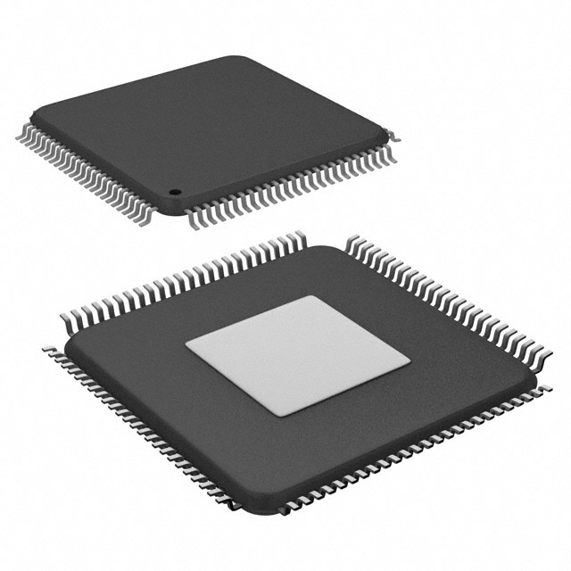
eTQFP64 (10 x 10 x 1.0 mm)
eTQFP100 (14 x 14 x 1.0 mm)
– Memory Error Management Unit (MEMU)
for collection and reporting of error events
in memories
– Cyclic redundancy check (CRC) unit
• Crossbar switch architecture for concurrent
access to peripherals, Flash, or RAM from
multiple bus masters with end-to-end ECC
eTQFP144 (20 x 20 x 1.0 mm) eLQFP176 (24 x 24 x 1.4 mm)
• Enhanced modular IO subsystem (eMIOS): up
to 64 timed I/O channels with 16-bit counter
resolution
FPBGA292 (17 x 17 x 1.8 mm)
Features
• AEC-Q100 qualified
• High performance e200z420n3 dual core
– 32-bit Power Architecture technology CPU
– Core frequency as high as 180 MHz
– Variable Length Encoding (VLE)
• 4224 KB (4096 KB code flash + 128 KB data
flash) on-chip flash memory: supports read
during program and erase operations, and
multiple blocks allowing EEPROM emulation
• 176 KB HSM dedicated flash memory (144 KB
code + 32 KB data)
• 384 KB on-chip general-purpose SRAM (in
addition to 128 KB core local data RAM: 64 KB
included in each CPU)
• Multi-channel direct memory access controller
(eDMA) with 64 channels
• 1 interrupt controller (INTC)
• Comprehensive new generation ASIL-B safety
concept
– ASIL-B of ISO 26262
– FCCU for collection and reaction to failure
notifications
May 2021
This is information on a product in full production.
• Body cross triggering unit (BCTU)
– Triggers ADC conversions from any eMIOS
channel
– Triggers ADC conversions from up to 2
dedicated PIT_RTIs
• Enhanced analog-to-digital converter system
with:
– 3 independent fast 12-bit SAR analog
converters
– 1 supervisor 12-bit SAR analog converter
– 1 10-bit SAR analog converter with STDBY
mode support
• Communication interfaces
– 18 LINFlexD modules
– 8 deserial serial peripheral interface (DSPI)
modules
– 8 MCAN interfaces with advanced shared
memory scheme and ISO CAN-FD support
– Dual-channel FlexRay controller
– 1 ethernet controller 10/100 Mbps,
compliant IEEE 802.3-2008
• Low power capabilities
– Versatile low power modes
– Ultra low power standby with RTC
– Smart Wake-up Unit for contact monitoring
– Fast wakeup schemes
• Dual phase-locked loops with stable clock
domain for peripherals and FM modulation
domain for computational shell
DS11620 Rev 8
1/153
www.st.com
�SPC584Cx, SPC58ECx
• Nexus development interface (NDI) per IEEE-ISTO 5001-2003 standard, with some
support for 2010 standard
• Boot assist Flash (BAF) supports factory programming using a serial bootload through the
asynchronous CAN or LIN/UART
• Junction temperature range -40 °C to 150 °C
Table 1. Device summary
Part number
Package
2 MB
Single core
eTQFP64
3 MB
Dual core
Single core
4 MB
Dual core
Single core
Dual core
SPC584C70E1 SPC58EC70E1 SPC584C74E1 SPC58EC74E1 SPC584C80E1 SPC58EC80E1
eTQFP100 SPC584C70E3 SPC58EC70E3 SPC584C74E3 SPC58EC74E3 SPC584C80E3 SPC58EC80E3
eTQFP144 SPC584C70E5 SPC58EC70E5 SPC584C74E5 SPC58EC74E5 SPC584C80E5 SPC58EC80E5
eLQFP176 SPC584C70E7 SPC58EC70E7 SPC584C74E7 SPC58EC74E7 SPC584C80E7 SPC58EC80E7
FPBGA292 SPC584C70C3 SPC58EC70C3 SPC584C74C3 SPC58EC74C3 SPC584C80C3 SPC58EC80C3
2/153
DS11620 Rev 8
�SPC584Cx, SPC58ECx
Contents
Contents
1
Introduction . . . . . . . . . . . . . . . . . . . . . . . . . . . . . . . . . . . . . . . . . . . . . . . . 6
2
Description . . . . . . . . . . . . . . . . . . . . . . . . . . . . . . . . . . . . . . . . . . . . . . . . . 7
2.1
Device feature summary . . . . . . . . . . . . . . . . . . . . . . . . . . . . . . . . . . . . . . 7
2.2
Block diagram . . . . . . . . . . . . . . . . . . . . . . . . . . . . . . . . . . . . . . . . . . . . . . . 8
2.3
Features overview . . . . . . . . . . . . . . . . . . . . . . . . . . . . . . . . . . . . . . . . . . .11
3
Package pinouts and signal descriptions . . . . . . . . . . . . . . . . . . . . . . . 13
4
Electrical characteristics . . . . . . . . . . . . . . . . . . . . . . . . . . . . . . . . . . . . 14
4.1
Introduction . . . . . . . . . . . . . . . . . . . . . . . . . . . . . . . . . . . . . . . . . . . . . . . 14
4.2
Absolute maximum ratings . . . . . . . . . . . . . . . . . . . . . . . . . . . . . . . . . . . . 15
4.3
Operating conditions . . . . . . . . . . . . . . . . . . . . . . . . . . . . . . . . . . . . . . . . 17
4.3.1
Power domains and power up/down sequencing . . . . . . . . . . . . . . . . . 19
4.4
Electrostatic discharge (ESD) . . . . . . . . . . . . . . . . . . . . . . . . . . . . . . . . . 20
4.5
Electromagnetic compatibility characteristics . . . . . . . . . . . . . . . . . . . . . . 21
4.6
Temperature profile . . . . . . . . . . . . . . . . . . . . . . . . . . . . . . . . . . . . . . . . . 22
4.7
Device consumption . . . . . . . . . . . . . . . . . . . . . . . . . . . . . . . . . . . . . . . . . 23
4.8
I/O pad specification . . . . . . . . . . . . . . . . . . . . . . . . . . . . . . . . . . . . . . . . . 26
4.8.1
I/O input DC characteristics . . . . . . . . . . . . . . . . . . . . . . . . . . . . . . . . . . 26
4.8.2
I/O output DC characteristics . . . . . . . . . . . . . . . . . . . . . . . . . . . . . . . . . 29
4.8.3
I/O pad current specifications . . . . . . . . . . . . . . . . . . . . . . . . . . . . . . . . 34
4.9
Reset pad (PORST) electrical characteristics . . . . . . . . . . . . . . . . . . . . . 37
4.10
PLLs . . . . . . . . . . . . . . . . . . . . . . . . . . . . . . . . . . . . . . . . . . . . . . . . . . . . . 40
4.11
4.12
4.10.1
PLL0 . . . . . . . . . . . . . . . . . . . . . . . . . . . . . . . . . . . . . . . . . . . . . . . . . . . 40
4.10.2
PLL1 . . . . . . . . . . . . . . . . . . . . . . . . . . . . . . . . . . . . . . . . . . . . . . . . . . . 42
Oscillators . . . . . . . . . . . . . . . . . . . . . . . . . . . . . . . . . . . . . . . . . . . . . . . . . 43
4.11.1
Crystal oscillator 40 MHz . . . . . . . . . . . . . . . . . . . . . . . . . . . . . . . . . . . . 43
4.11.2
Crystal Oscillator 32 kHz . . . . . . . . . . . . . . . . . . . . . . . . . . . . . . . . . . . . 44
4.11.3
RC oscillator 16 MHz . . . . . . . . . . . . . . . . . . . . . . . . . . . . . . . . . . . . . . . 45
4.11.4
Low power RC oscillator . . . . . . . . . . . . . . . . . . . . . . . . . . . . . . . . . . . . 46
ADC system . . . . . . . . . . . . . . . . . . . . . . . . . . . . . . . . . . . . . . . . . . . . . . . 47
4.12.1
ADC input description . . . . . . . . . . . . . . . . . . . . . . . . . . . . . . . . . . . . . . 47
DS11620 Rev 8
3/153
5
�Contents
SPC584Cx, SPC58ECx
SAR ADC 12-bit electrical specification . . . . . . . . . . . . . . . . . . . . . . . . . 48
4.12.3
SAR ADC 10-bit electrical specification . . . . . . . . . . . . . . . . . . . . . . . . . 53
4.13
Temperature Sensor . . . . . . . . . . . . . . . . . . . . . . . . . . . . . . . . . . . . . . . . . 56
4.14
LFAST pad electrical characteristics . . . . . . . . . . . . . . . . . . . . . . . . . . . . 57
4.15
5
4.12.2
4.14.1
LFAST interface timing diagrams . . . . . . . . . . . . . . . . . . . . . . . . . . . . . . 57
4.14.2
LFAST LVDS interface electrical characteristics . . . . . . . . . . . . . . . . . . 58
4.14.3
LFAST PLL electrical characteristics . . . . . . . . . . . . . . . . . . . . . . . . . . . 61
Power management . . . . . . . . . . . . . . . . . . . . . . . . . . . . . . . . . . . . . . . . . 63
4.15.1
Power management integration . . . . . . . . . . . . . . . . . . . . . . . . . . . . . . . 63
4.15.2
Voltage regulators . . . . . . . . . . . . . . . . . . . . . . . . . . . . . . . . . . . . . . . . . 69
4.15.3
Voltage monitors . . . . . . . . . . . . . . . . . . . . . . . . . . . . . . . . . . . . . . . . . . 70
4.16
Flash . . . . . . . . . . . . . . . . . . . . . . . . . . . . . . . . . . . . . . . . . . . . . . . . . . . . 73
4.17
AC Specifications . . . . . . . . . . . . . . . . . . . . . . . . . . . . . . . . . . . . . . . . . . . 77
4.17.1
Debug and calibration interface timing . . . . . . . . . . . . . . . . . . . . . . . . . 77
4.17.2
DSPI timing with CMOS pads . . . . . . . . . . . . . . . . . . . . . . . . . . . . . . . . 83
4.17.3
Ethernet timing . . . . . . . . . . . . . . . . . . . . . . . . . . . . . . . . . . . . . . . . . . . . 93
4.17.4
FlexRay timing . . . . . . . . . . . . . . . . . . . . . . . . . . . . . . . . . . . . . . . . . . . . 99
4.17.5
CAN timing . . . . . . . . . . . . . . . . . . . . . . . . . . . . . . . . . . . . . . . . . . . . . . 103
4.17.6
UART timing . . . . . . . . . . . . . . . . . . . . . . . . . . . . . . . . . . . . . . . . . . . . . 103
4.17.7
I2C timing . . . . . . . . . . . . . . . . . . . . . . . . . . . . . . . . . . . . . . . . . . . . . . . 104
Package information . . . . . . . . . . . . . . . . . . . . . . . . . . . . . . . . . . . . . . . 106
5.1
eTQFP64 package information . . . . . . . . . . . . . . . . . . . . . . . . . . . . . . . 106
5.1.1
5.2
eTQFP100 package information . . . . . . . . . . . . . . . . . . . . . . . . . . . . . . . 111
5.2.1
5.3
4/153
Package mechanical drawings and data information . . . . . . . . . . . . . 125
FPBGA292 package information . . . . . . . . . . . . . . . . . . . . . . . . . . . . . . 126
5.5.1
5.6
Package mechanical drawings and data information . . . . . . . . . . . . . 120
eLQFP176 package information . . . . . . . . . . . . . . . . . . . . . . . . . . . . . . . 121
5.4.1
5.5
Package mechanical drawings and data information . . . . . . . . . . . . . 115
eTQFP144 package information . . . . . . . . . . . . . . . . . . . . . . . . . . . . . . .116
5.3.1
5.4
Package mechanical drawings and data information . . . . . . . . . . . . . 110
Package mechanical drawings and data information . . . . . . . . . . . . . 128
Package thermal characteristics . . . . . . . . . . . . . . . . . . . . . . . . . . . . . . 130
5.6.1
eTQFP64 . . . . . . . . . . . . . . . . . . . . . . . . . . . . . . . . . . . . . . . . . . . . . . . 130
5.6.2
eTQFP100 . . . . . . . . . . . . . . . . . . . . . . . . . . . . . . . . . . . . . . . . . . . . . . 130
5.6.3
eTQFP144 . . . . . . . . . . . . . . . . . . . . . . . . . . . . . . . . . . . . . . . . . . . . . . 131
DS11620 Rev 8
�SPC584Cx, SPC58ECx
Contents
5.6.4
LQFP176 . . . . . . . . . . . . . . . . . . . . . . . . . . . . . . . . . . . . . . . . . . . . . . . 132
5.6.5
FPBGA292 . . . . . . . . . . . . . . . . . . . . . . . . . . . . . . . . . . . . . . . . . . . . . . 133
5.6.6
General notes for specifications at maximum junction temperature . . 133
6
Ordering information . . . . . . . . . . . . . . . . . . . . . . . . . . . . . . . . . . . . . . 136
7
Revision history . . . . . . . . . . . . . . . . . . . . . . . . . . . . . . . . . . . . . . . . . . 140
DS11620 Rev 8
5/153
5
�Introduction
1
SPC584Cx, SPC58ECx
Introduction
This document describes the features of the family and options available within the family
members, and highlights important electrical and physical characteristics of the device. To
ensure a complete understanding of the device functionality, refer also to the device
reference manual and errata sheet.
6/153
DS11620 Rev 8
�SPC584Cx, SPC58ECx
2
Description
Description
The SPC584Cx and SPC58ECx microcontroller is the first in a new family of devices
superseding the SPC564Cx and SPC56ECx family. SPC584Cx and SPC58ECx builds on
the legacy of the SPC564Cx and SPC56ECx family, while introducing new features coupled
with higher throughput to provide substantial reduction of cost per feature and significant
power and performance improvement (MIPS per mW). On the SPC584Cx and SPC58ECx
device, there are two processor cores e200z420 and one e200z0 core embedded in the
Hardware Security Module.
2.1
Device feature summary
Table 2 lists a summary of major features for the SPC584Cx and SPC58ECx device. The
feature column represents a combination of module names and capabilities of certain
modules. A detailed description of the functionality provided by each on-chip module is
given later in this document.
Table 2. Features List
Feature
Description
SPC58 family
40 nm
Number of Cores
2
Local RAM
2x 64 KB Data
Single Precision Floating Point
Yes
SIMD
No
VLE
Yes
8 KB Instruction
Cache
4 KB Data
Core MPU: 24 per CPU
MPU
System MPU: 24 per XBAR
Semaphores
Yes
CRC Channels
2x4
Software Watchdog Timer (SWT)
3
Core Nexus Class
3+
4 x SCU
Event Processor
4 x PMC
Run control Module
Yes
System SRAM
384 KB (including 256 KB of standby RAM)
Flash
4096 KB code / 128 KB data
Flash fetch accelerator
2 x 4 x 256-bit
DMA channels
64
DS11620 Rev 8
7/153
12
�Description
SPC584Cx, SPC58ECx
Table 2. Features List (continued)
Feature
Description
DMA Nexus Class
3
LINFlexD
18
MCAN (ISO CAN-FD compliant)
8
DSPI
8
I2C
1
FlexRay
1 x Dual channel
Ethernet
1 MAC with Time Stamping, AVB and VLAN support
SIPI / LFAST Debugger
High Speed
8 PIT channels
System Timers
4 AUTOSAR® (STM)
RTC/API
eMIOS
2 x 32 channels
BCTU
64 channels
Interrupt controller
1 x 568 sources
ADC (SAR)
5
Temp. sensor
Yes
Self Test Controller
Yes
PLL
Dual PLL with FM
Integrated linear voltage regulator
Yes
External Power Supplies
5 V, 3.3 V
HALT Mode
Low Power Modes
STOP Mode
Smart Standby with output controller, analog and digital inputs
Standby Mode
2.2
Block diagram
The figures below show the top-level block diagrams.
8/153
DS11620 Rev 8
�SPC584Cx, SPC58ECx
Description
Figure 1. Block diagram
JTAGM
JTAGC
DCI
SPU
NPC
INTC
SWT_0 IAC
D-MEM
Control
D-Cache
Control
64 KB
D-MEM
4 KB
2 way
Core Memory Protection Unit
(CMPU)
BIU with E2E ECC
Decorated Storage Access
S6
Instruction
32 ADD
64 DATA
Load / Store
32 ADD
64 DATA
M0
M1
DMA CHMUX_3
DMA CHMUX_2
DMA CHMUX_1
DMA CHMUX_0
64 Ch
eDMA_1
32 ADD
64 DATA
Concentrator_1
E2E ECC
PAMU
VLE
Delayed Lock-step with Redundancy Checkers
8 KB
2 way
SIPI_1
Unified
Backdoor
Interface
With
E2E ECC
FlexRay_0
I-Cache
Control
ETHERNET_0
EFPU2
Delayed Lock-step with Redundancy Checkers
VLE
Nexus3p
Nexus3p
e200 z420n3 – 180 MHz
dual issue
Main Core_0
EFPU2
I-Cache
Control
8 KB
2 way
HSM
D-MEM
Control
D-Cache
Control
64 KB
D-MEM
4 KB
2 way
Unified
Backdoor
Interface
With
E2E ECC
Core Memory Protection Unit
(CMPU)
Delayed Lock-step with Redundancy Checkers
SWT_2 IAC
e200 z420n3 – 180 MHz
dual issue
Main Core_2
BIU with E2E ECC
Decorated Storage Access
Nexus Data
Trace
Nexus Data
Trace
Nexus Data
Trace
32 ADD
64 DATA
32 ADD
64 DATA
32 ADD
64 DATA
Instruction
32 ADD
64 DATA
Load / Store
32 ADD
64 DATA
M3
M2
M6
M4
M5
Cross Bar Switch (XBAR) AMBA 2.0 v6 AHB – 64 bits
System Memory Protection Unit
S3
S2
S5
S4
32 ADD
64 DATA
32 ADD
64 DATA
32 ADD
64 DATA
32 ADD
64 DATA
Periph.
Bridge 2
E2E ECC
Periph.
Bridge 1
E2E ECC
PRAMC_2
with E2E
ECC
PRAMC_3
with E2E
ECC
32 ADD
32 DATA
32 ADD
32 DATA
32 ADD
64 DATA
32 ADD
64 DATA
Peripheral
Cluster 2
Peripheral
Cluster 1
SRAM
Array 2
256 KB
SRAM
Array 3
128 KB
DS11620 Rev 8
S0
32 ADD
64 DATA
S7
S1
32 ADD
64 DATA
PFLASHC_1
Set-Associative Prefetch
Buffers
with E2E ECC
256 Page Line
FLASH
4 MB
EEPROM
4x32 KB
Non Volatile Memory
Multiple RWW partitions
9/153
12
�Description
SPC584Cx, SPC58ECx
Figure 2. Periphery allocation
BCTU_0
PBRIDGE_2
STDBY_CTU_0
XBAR_1
eMIOS_0
XBIC_Concentrator_1
ETHERNET_0
SMPU_1
SAR_ADC_12bit_0
XBIC_1
SAR_ADC_10bit_STDBY
PCM_0
SAR_ADC_12bit_B0
PFLASH_1
FLEXRAY_0
SEM42
I2C_0
INTC_1
DSPI_0, 2, 4, 6
SWT_0, 2, 3
LINFlexD_0, 2, 4, 6, 8, 10, 12,14,16
STM_0, 2
CAN_SUB_0_MESSAGE_RAM
eDMA_1
CAN_SUB_0_M_CAN_0..3
PRAM_2, 3
CCCU
TDM_0
HSM
DTS
JDC
JTAGM
MEMU
IMA
CRC_0
DMAMUX_0, 2
PIT_0
RTC/API
WKPU
MC_PCU
PBRIDGE_2 – Peripheral Cluster 2
STCU
DSPI_1, 3, 5, 7
LINFlexD_1, 3, 5, 7, 9, 11, 13, 15, 17
MC_RGM
CAN_SUB_1_MESSAGE_RAM
RCOSC_DIG
CAN_SUB_1_M_CAN_1..4
RC1024K_DIG
FCCU
OSC_DIG
CRC_1
OSC32K_DIG
DMAMUX_1, 3
PLL_DIG
PIT_1
CMU_0_PLL0_XOSC_IRCOSC
CMU_1_CORE_XBAR
MC_CGM
CMU_2_HPBM
MC_ME
CMU_3_PBRIDGE
SIUL2
CMU_6_SARADC
FLASH_0
CMU_11_FBRIDGE
FLASH_ALT_0
CMU_12_EMIOS
PASS
CMU_14_PFBRIDGE
PBRIDGE_1 – Peripheral Cluster 1
PMC_DIG
SSCM
PBRIDGE_1
eMIOS_1
SAR_ADC_12bit_1, 3
SIPI_1
LFAST_1
Note: In this diagram, ON-platform modules are shown in orange color and OFF-platform modules
are shown in blue color.
10/153
DS11620 Rev 8
�SPC584Cx, SPC58ECx
2.3
Description
Features overview
On-chip modules within SPC584Cx and SPC58ECx include the following features:
•
•
Two main CPUs, dual issue, 32-bit CPU core complexes (e200z4).
–
Power Architecture embedded specification compliance
–
Instruction set enhancement allowing variable length encoding (VLE), encoding a
mix of 16-bit and 32-bit instructions, for code size footprint reduction
–
Single-precision floating point operations
–
64 KB local data RAM for Core_0 and Core_2
–
8 KB I-Cache and 4 KB D-Cache for Core_0 and Core_2
4224 KB (4096 KB code flash + 128 KB data flash) on-chip flash memory
–
Supports read during program and erase operations, and multiple blocks allowing
EEPROM emulation
•
176 KB HSM dedicated flash memory (144 KB code + 32 KB data)
•
384 KB on-chip general-purpose SRAM (+ 128 KB local data RAM: 64 KB included in
each CPU)
•
Multi channel direct memory access controllers
–
64 eDMA channels
•
One interrupt controller (INTC)
•
Dual phase-locked loops with stable clock domain for peripherals and FM modulation
domain for computational shell
•
Crossbar switch architecture for concurrent access to peripherals, Flash, or RAM from
multiple bus masters with end-to-end ECC
•
Hardware security module (HSM) with HW cryptographic co-processor
•
System integration unit lite (SIUL)
•
Boot assist Flash (BAF) supports factory programming using a serial bootload through
the asynchronous CAN or LIN/UART.
•
Hardware support for safety ASIL-B level related applications
•
Enhanced modular IO subsystem (eMIOS): up to 64 (2 x 32) timed I/O channels with
16-bit counter resolution
•
•
–
Buffered updates
–
Support for shifted PWM outputs to minimize occurrence of concurrent edges
–
Supports configurable trigger outputs for ADC conversion for synchronization to
channel output waveforms
–
Shared or independent time bases
–
DMA transfer support available
Body cross triggering unit (BCTU)
–
Triggers ADC conversions from any eMIOS channel
–
Triggers ADC conversions from up to 2 dedicated PIT_RTIs
–
One event configuration register dedicated to each timer event allows to define the
corresponding ADC channel
–
Synchronization with ADC to avoid collision
Enhanced analog-to-digital converter system with:
–
Three independent fast 12-bit SAR analog converters
DS11620 Rev 8
11/153
12
�Description
12/153
SPC584Cx, SPC58ECx
–
One supervisor 12-bit SAR analog converter
–
One 10-bit SAR analog converter with STDBY mode support
•
Eight deserial serial peripheral interface (DSPI) modules
•
Eighteen LIN and UART communication interface (LINFlexD) modules
–
LINFlexD_0 is a Master/Slave
–
All others are Masters
•
Eight modular controller area network (MCAN) modules, all supporting flexible data
rate (ISO CAN-FD compliant)
•
Dual-channel FlexRay controller
•
One ethernet controller 10/100 Mbps, compliant IEEE 802.3-2008
–
IEEE 1588-2008 Time stamping (internal 64-bit time stamp)
–
IEEE 802.1AS and IEEE 802.1Qav (AVB-Feature)
–
IEEE 802.1Q VLAN tag detection
–
IPv4 and IPv6 checksum modules
•
Nexus development interface (NDI) per IEEE-ISTO 5001-2003 standard, with some
support for 2010 standard.
•
Device and board test support per Joint Test Action Group (JTAG) (IEEE 1149.1 and
IEEE 1149.7), 2-pin JTAG interface.
•
Standby power domain with smart wake-up sequence
DS11620 Rev 8
�SPC584Cx, SPC58ECx
3
Package pinouts and signal descriptions
Package pinouts and signal descriptions
Refer to the SPC584Cx and SPC58ECx IO_ Definition document.
It includes the following sections:
1.
Package pinouts
2.
Pin descriptions
a)
Power supply and reference voltage pins
b)
System pins
c)
LVDS pins
d)
Generic pins
DS11620 Rev 8
13/153
13
�Electrical characteristics
SPC584Cx, SPC58ECx
4
Electrical characteristics
4.1
Introduction
The present document contains the target Electrical Specification for the 40 nm family 32-bit
MCU SPC584Cx and SPC58ECx products.
In the tables where the device logic provides signals with their respective timing
characteristics, the symbol “CC” (Controller Characteristics) is included in the “Symbol”
column.
In the tables where the external system must provide signals with their respective timing
characteristics to the device, the symbol “SR” (System Requirement) is included in the
“Symbol” column.
The electrical parameters shown in this document are guaranteed by various methods. To
give the customer a better understanding, the classifications listed in Table 3 are used and
the parameters are tagged accordingly in the tables where appropriate.
Table 3. Parameter classifications
Classification tag
14/153
Tag description
P
Those parameters are guaranteed during production testing on each individual device.
C
Those parameters are achieved by the design characterization by measuring a statistically
relevant sample size across process variations.
T
Those parameters are achieved by design validation on a small sample size from typical
devices.
D
Those parameters are derived mainly from simulations.
DS11620 Rev 8
�SPC584Cx, SPC58ECx
4.2
Electrical characteristics
Absolute maximum ratings
Table 4 describes the maximum ratings for the device. Absolute maximum ratings are stress
ratings only, and functional operation at the maxima is not guaranteed. Exposure to
absolute maximum rating conditions for extended periods may affect device reliability.
Stress beyond the listed maxima, even momentarily, may affect device reliability or cause
permanent damage to the device.
Table 4. Absolute maximum ratings
Value
Symbol
C
Parameter
Conditions
Unit
Min
Typ
Max
VDD_LV
SR
D
Core voltage
operating life
range(1)
—
–0.3
—
1.4
V
VDD_HV_IO_MAIN
VDD_HV_IO_FLEX
VDD_HV_OSC
VDD_HV_FLA
SR
D
I/O supply
voltage(2)
—
–0.3
—
6.0
V
VSS_HV_ADV
SR
D
ADC ground
voltage
Reference to
digital ground
–0.3
—
0.3
V
VDD_HV_ADV
SR
D
ADC Supply
voltage(2)
Reference to
VSS_HV_ADV
–0.3
—
6.0
V
VSS_HV_ADR_S
SR
D
SAR ADC
ground
reference
—
–0.3
—
0.3
V
VDD_HV_ADR_S
SR
D
SAR ADC
voltage
reference(2)
Reference to
VSS_HV_ADR_S
–0.3
—
6.0
V
VSS-VSS_HV_ADR_S
SR
D
VSS_HV_ADR_S
differential
voltage
—
–0.3
—
0.3
V
VSS-VSS_HV_ADV
SR
D
VSS_HV_ADV
differential
voltage
—
–0.3
—
0.3
V
—
–0.3
—
6.0
Relative to Vss
–0.3
—
—
Relative to
VDD_HV_IO and
VDD_HV_ADV
—
—
0.3
VIN
TTRIN
IINJ
SR
SR
SR
D
I/O input voltage
range(2)(3) (4)
V
D
Digital Input pad
transition time(5)
—
—
—
1
ms
T
Maximum DC
injection current
for each
analog/digital
PAD(6)
—
–5
—
5
mA
DS11620 Rev 8
15/153
16
�Electrical characteristics
SPC584Cx, SPC58ECx
Table 4. Absolute maximum ratings (continued)
Value
Symbol
TSTG
TPAS
C
SR
SR
Parameter
Conditions
Unit
Min
Typ
Max
T
Maximum nonoperating
Storage
temperature
range
—
–55
—
125
°C
C
Maximum nonoperating
temperature
during passive
lifetime
—
–55
—
150(7)
°C
—
—
20
years
TSTORAGE
SR
—
Maximum
No supply; storage
storage time,
temperature in
assembled part
range –40 °C to
programmed in
60 °C
ECU
TSDR
SR
T
Maximum solder
temperature Pbfree packaged(8)
—
—
—
260
°C
MSL
SR
T
Moisture
sensitivity
level(9)
—
—
—
3
—
Maximum
cumulated
XRAY dose
Typical range for
X-rays source
during
inspection:80 ÷
130 KV; 20 ÷
50 μA
—
—
1
grey
TXRAY dose
SR
T
1. VDD_LV: allowed 1.335 V - 1.400 V for 60 seconds cumulative time at the given temperature profile. Remaining time allowed
1.260 V - 1.335 V for 10 hours cumulative time at the given temperature profile. Remaining time as defined in Section 4.3:
Operating conditions.
2. VDD_HV: allowed 5.5 V – 6.0 V for 60 seconds cumulative time at the given temperature profile, for 10 hours cumulative
time with the device in reset at the given temperature profile. Remaining time as defined in Section 4.3: Operating
conditions.
3. The maximum input voltage on an I/O pin tracks with the associated I/O supply maximum. For the injection current
condition on a pin, the voltage will be equal to the supply plus the voltage drop across the internal ESD diode from I/O pin
to supply. The diode voltage varies greatly across process and temperature, but a value of 0.3 V can be used for nominal
calculations.
4. Relative value can be exceeded if design measures are taken to ensure injection current limitation (parameter IINJ).
5. This limitation applies to pads with digital input buffer enabled. If the digital input buffer is disabled, there are no maximum
limits to the transition time.
6. The limits for the sum of all normal and injected currents on all pads within the same supply segment can be found in
Section 4.8.3: I/O pad current specifications.
7. 175°C are allowed for limited time. Mission profile with passive lifetime temperature >150°C have to be evaluated by ST to
confirm that are granted by product qualification.
8. Solder profile per IPC/JEDEC J-STD-020D.
9. Moisture sensitivity per JDEC test method A112.
16/153
DS11620 Rev 8
�SPC584Cx, SPC58ECx
4.3
Electrical characteristics
Operating conditions
Table 5 describes the operating conditions for the device, and for which all the specifications
in the data sheet are valid, except where explicitly noted. The device operating conditions
must not be exceeded or the functionality of the device is not guaranteed.
Table 5. Operating conditions
Value(1)
Symbol
C
Parameter
Conditions
Unit
Min
Typ
Max
FSYS(2)
SR
P
Operating
system clock
frequency(3)
—
—
—
180
MHz
TA_125 Grade(4)
SR
D
Operating
Ambient
temperature
—
–40
—
125
°C
TJ_125 Grade(4)
SR
P
Junction
temperature
under bias
TA = 125 °C
–40
—
150
°C
TA_105 Grade(4)
SR
D
Ambient
temperature
under bias
—
–40
—
105
°C
TJ_105 Grade(4)
SR
D
Operating
Junction
temperature
TA = 105 °C
–40
—
130
°C
VDD_LV
SR
P
Core supply
voltage(5)
—
1.14
1.20
1.26(6) (7)
V
VDD_HV_IO_MAIN
VDD_HV_IO_FLEX
VDD_HV_FLA
VDD_HV_OSC
SR
P
IO supply
voltage
—
3.0
—
5.5
V
VDD_HV_ADV
SR
P
ADC supply
voltage
—
3.0
—
5.5
V
VSS_HV_ADVVSS
SR
D
ADC ground
differential
voltage
—
–25
—
25
mV
VDD_HV_ADR_S
SR
P
SAR ADC
reference
voltage
—
3.0
—
5.5
V
D
SAR ADC
reference
differential
voltage
—
—
—
25
mV
P
SAR ADC
ground
reference
voltage
—
VDD_HV_ADR_SVDD_HV_ADV
VSS_HV_ADR_S
SR
SR
DS11620 Rev 8
VSS_HV_ADV
V
17/153
19
�Electrical characteristics
SPC584Cx, SPC58ECx
Table 5. Operating conditions (continued)
Value(1)
Symbol
C
Parameter
Conditions
Unit
Min
Typ
Max
VSS_HV_ADR_SVSS_HV_ADV
SR
D
VSS_HV_ADR_S
differential
voltage
—
–25
—
25
mV
VRAMP_HV
SR
D
Slew rate on
HV power
supply
—
—
—
100
V/ms
VIN
SR
P
I/O input
voltage range
—
0
—
5.5
V
Digital pins and
analog pins
–3.0
—
3.0
mA
Digital pins and
analog pins
–10
—
10
mA
IINJ1
SR
T
Injection
current (per
pin) without
performance
degradation(8)
(9) (10)
IINJ2
SR
D
Dynamic
Injection
current (per
pin) with
performance
degradation(10)
(11)
1. The ranges in this table are design targets and actual data may vary in the given range.
2. The maximum number of PRAM wait states has to be configured accordingly to the system clock frequency. Refer to
Table 6.
3. Maximum operating frequency is applicable to the cores and platform of the device. See the Clock Chapter in the
Microcontroller Reference Manual for more information on the clock limitations for the various IP blocks on the device.
4. In order to evaluate the actual difference between ambient and junction temperatures in the application, refer to
Section 5.6: Package thermal characteristics.
5. Core voltage as measured on device pin to guarantee published silicon performance.
6. Core voltage can exceed 1.26 V with the limitations provided in Section 4.2: Absolute maximum ratings, provided that
HVD134_C monitor reset is disabled.
7. 1.260 V - 1.290 V range allowed periodically for supply with sinusoidal shape and average supply value below or equal to
1.236 V at the given temperature profile.
8. Full device lifetime. I/O and analog input specifications are only valid if the injection current on adjacent pins is within these
limits. See Section 4.2: Absolute maximum ratings for maximum input current for reliability requirements.
9. The I/O pins on the device are clamped to the I/O supply rails for ESD protection. When the voltage of the input pins is
above the supply rail, current will be injected through the clamp diode to the supply rails. For external RC network
calculation, assume typical 0.3 V drop across the active diode. The diode voltage drop varies with temperature.
10. The limits for the sum of all normal and injected currents on all pads within the same supply segment can be found in
Section 4.8.3: I/O pad current specifications.
11. Positive and negative Dynamic current injection pulses are allowed up to this limit. I/O and ADC specifications are not
granted. See the dedicated chapters for the different specification limits. See the Absolute Maximum Ratings table for
maximum input current for reliability requirements. Refer to the following pulses definitions: Pulse1 (ISO 7637-2:2011),
Pulse 2a(ISO 7637-2:2011 5.6.2), Pulse 3a (ISO 7637-2:2011 5.6.3), Pulse 3b (ISO 7637-2:2011 5.6.3).
18/153
DS11620 Rev 8
�SPC584Cx, SPC58ECx
Electrical characteristics
Table 6. PRAM wait states configuration
4.3.1
PRAMC WS
Clock Frequency (MHz)
1
< 180
0
< 120
Power domains and power up/down sequencing
The following table shows the constraints and relationships for the different power domains.
Supply1 (on rows) can exceed Supply2 (on columns), only if the cell at the given row and
column is reporting ‘ok’. This limitation is valid during power-up and power-down phases, as
well as during normal device operation.
Table 7. Device supply relation during power-up/power-down sequence
Supply2
Supply1
VDD_LV
VDD_HV_IO_FLEX
VDD_HV_IO_MAIN
VDD_HV_FLA
VDD_HV_OSC
VDD_HV_ADV
VDD_HV_ADR
not allowed
ok
ok
ok
ok
VDD_HV_IO_FLEX
ok
VDD_HV_IO_MAIN
VDD_HV_FLA
VDD_HV_OSC
ok
ok
VDD_HV_ADV
ok
ok
not allowed
VDD_HV_ADR
ok
ok
not allowed
ok
not allowed
During power-up, all functional terminals are maintained in a known state as described in
the device pinout Microsoft Excel file attached to the IO_Definition document.
DS11620 Rev 8
19/153
19
�Electrical characteristics
4.4
SPC584Cx, SPC58ECx
Electrostatic discharge (ESD)
The following table describes the ESD ratings of the device:
•
All ESD testing are in conformity with CDF-AEC-Q100 Stress Test Qualification for
Automotive Grade Integrated Circuits,
•
Device failure is defined as: “If after exposure to ESD pulses, the device does not meet
the device specification requirements, which include the complete DC parametric and
functional testing at room temperature and hot temperature, maximum DC parametric
variation within 10% of maximum specification”.
Table 8. ESD ratings
Parameter
ESD for Human Body Model (HBM)(1)
ESD for field induced Charged Device Model (CDM)(2)
C
Conditions
Value
Unit
T
All pins
2000
V
T
All pins
500
V
T
Corner Pins
750
V
1. This parameter tested in conformity with ANSI/ESD STM5.1-2007 Electrostatic Discharge Sensitivity Testing.
2. This parameter tested in conformity with ANSI/ESD STM5.3-1990 Charged Device Model - Component Level.
20/153
DS11620 Rev 8
�SPC584Cx, SPC58ECx
4.5
Electrical characteristics
Electromagnetic compatibility characteristics
EMC measurements at IC-level IEC standards are available from STMicroelectronics on
request.
DS11620 Rev 8
21/153
21
�Electrical characteristics
4.6
SPC584Cx, SPC58ECx
Temperature profile
The device is qualified in accordance to AEC-Q100 Grade1 requirements, such as HTOL
1,000 h and HTDR 1,000 hrs, TJ = 150 °C.
Mission profile exceeding AEC-Q100 Grade 1, and with junction Temperature equal to or
lower than 150 °C have to be evaluated by ST to confirm that are covered by product
qualification. Contact your STMicroelectronics Sales representative for validation.
22/153
DS11620 Rev 8
�SPC584Cx, SPC58ECx
4.7
Electrical characteristics
Device consumption
Table 9. Device consumption
Value(1)
Symbol
IDD_LKG(2),(3)
C
CC
Parameter
Conditions
Unit
Min
Typ
Max
C
TJ = 40 °C
—
—
14
D
TJ = 25 °C
—
—
10
D Leakage current on the
VDD_LV supply
D
TJ = 55 °C
—
—
20
TJ = 95 °C
—
—
50
D
TJ = 120 °C
—
—
90
P
TJ = 150 °C
—
—
180
—
—
—
210
mA
mA
IDD_LV(3)
CC
P
Dynamic current on
the VDD_LV supply,
very high consumption
profile(4)
IDD_HV
CC
P
Total current on the
VDD_HV supply(4)
fMAX
—
—
64
mA
IDD_LV_GW
CC
T
Dynamic current on
the VDD_LV supply,
gateway profile(5)
—
—
—
170
mA
IDD_HV_GW
CC
T
Dynamic current on
the VDD_HV supply,
gateway profile(5)
—
—
—
37
mA
IDD_LV_BCM
CC
T
Dynamic current on
the VDD_LV supply,
body profile(6)
—
—
—
150
mA
IDD_HV_BCM
CC
T
Dynamic current on
the VDD_HV supply,
body profile(6)
—
—
—
44
mA
IDD_MAIN_CORE_AC
CC
T
Main Core dynamic
current(7)
fMAX
—
—
50
mA
IDD_HSM_AC
CC
T
HSM platform dynamic
operating current(8)
fMAX/2
—
—
20
mA
T
Dynamic current on
the VDD_LV supply
+Total current on the
VDD_HV supply
—
—
71
100
mA
T
Dynamic current on
the VDD_LV supply
+Total current on the
VDD_HV supply
—
—
15
30
mA
IDDHALT(9)
IDDSTOP(10)
CC
CC
DS11620 Rev 8
23/153
25
�Electrical characteristics
SPC584Cx, SPC58ECx
Table 9. Device consumption (continued)
Value(1)
Symbol
C
Parameter
Typ
Max
TJ = 25 °C
—
85
160
TJ = 40 °C
—
—
250
TJ = 55 °C
—
—
370
TJ = 120 °C
—
1.2
2.2
P
TJ = 150 °C
—
2.9
5.0
D
TJ = 25 °C
—
100
180
TJ = 40 °C
—
—
270
TJ = 55 °C
—
—
410
TJ = 120 °C
—
—
2.4
P
TJ = 150 °C
—
—
5.5
D
TJ = 25 °C
—
150
250
TJ = 40 °C
—
—
390
TJ = 55 °C
—
—
590
TJ = 120 °C
—
2.0
3.5
TJ = 150 °C
—
5.1
8
D
SSWU running over all
STANDBY period with
OPC/TU commands
execution and keeping
ADC off(12)
TJ = 40 °C
—
1.0
3.5
mA
D
SSWU running over all
STANDBY period with
OPC/TU/ADC
commands execution
and keeping ADC
on(13)
TJ = 40 °C
—
3.5
5.0
mA
C
CC
D
D
C
IDDSTBY32
CC
D
D
C
IDDSTBY256
CC
D
D
Total standby mode
current on VDD_LV and
VDD_HV supply, 8 KB
RAM(11)
Total standby mode
current on VDD_LV and
VDD_HV supply, 32 KB
RAM(11)
Total standby mode
current on VDD_LV and
VDD_HV supply,
256 KB RAM(11)
P
IDDSSWU1
IDDSSWU2
CC
CC
Unit
Min
D
IDDSTBY8
Conditions
µA
mA
µA
mA
µA
mA
1. The ranges in this table are design targets and actual data may vary in the given range.
2. The leakage considered is the sum of core logic and RAM memories. The contribution of analog modules is not considered,
and they are computed in the dynamic IDD_LV and IDD_HV parameters.
3. IDD_LKG (leakage current) and IDD_LV (dynamic current) are reported as separate parameters, to give an indication of the
consumption contributors. The tests used in validation, characterization and production are verifying that the total
consumption (leakage+dynamic) is lower or equal to the sum of the maximum values provided (IDD_LKG + IDD_LV). The two
parameters, measured separately, may exceed the maximum reported for each, depending on the operative conditions and
the software profile used.
4. Use case: 2 x e200Z4 @180 MHz, HSM @90 MHz, all IPs clock enabled, Flash access with prefetch disabled, Flash
consumption includes parallel read and program/erase, all SARADC in continuous conversion, DMA continuously triggered
by ADC conversion, 4 DSPI / 8 CAN / 2 LINFlex and 2 DSPI transmitting, 2 x EMIOS running (8 channels in OPWMT
mode), FIRC, SIRC, FXOSC, PLL0-1 running. The switching activity estimated for dynamic consumption does not include
I/O toggling, which is highly dependent on the application. Details of the software configuration are available separately.
The total device consumption is IDD_LV + IDD_HV + IDD_LKG for the selected temperature.
5. Gateway use case: Two cores running at 160 MHz, DMA, PLL, FLASH read only 25%, 8xCAN, 1xEthernet, HSM,
2xSARADC.
6. BCM use case: One Core running at 160 MHz, no lockstep no, DMA, PLL, FLASH read only 25%, 2xCAN, HSM,
4xSARADC.
24/153
DS11620 Rev 8
�SPC584Cx, SPC58ECx
Electrical characteristics
7. Dynamic consumption of one core, including the dedicated I/D-caches and I/D-MEMS contribution.
8. Dynamic consumption of the HSM module, including the dedicated memories, during the execution of Electronic Code
Book crypto algorithm on 1 block of 16 byte of shared RAM.
9. Flash in Low Power. Sysclk at 160 MHz, PLL0_PHI at 160 MHz, XTAL at 40 MHz, FIRC 16 MHz ON, RCOSC1M off.
FlexCAN: instances: 0, 1, 2, 3, 4, 5, 6, 7 ON (configured but no reception or transmission), Ethernet ON (configured but no
reception or transmission), ADC ON (continuously converting). All others IPs clock-gated.
10. Sysclk = RC16 MHz, RC16 MHz ON, RC1 MHz ON, PLL OFF. All possible peripherals off and clock gated. Flash in power
down mode.
11. STANDBY mode: device configured for minimum consumption, RC16 MHz off, RC1 MHz on, OSC32K off, SSWU off.
12. SSWU1 mode adder: FIRC = ON, SSWU clocked at 8 MHz and running over all STANDBY period, ADC off. The total
standby consumption can be obtained by adding this parameter to the IDDSTBY parameter for the selected memory size
and temperature.
13. SSWU2 mode adder: FIRC = ON, SSWU clocked at 8 MHz and running over all STANDBY period, ADC on in continuous
conversion. The total standby consumption can be obtained by adding this parameter to the IDDSTBY parameter for the
selected memory size and temperature.
DS11620 Rev 8
25/153
25
�Electrical characteristics
4.8
SPC584Cx, SPC58ECx
I/O pad specification
The following table describes the different pad type configurations.
Table 10. I/O pad specification descriptions
Pad type
Description
Weak configuration
Provides a good compromise between transition time and low electromagnetic emission.
Medium configuration
Strong configuration
Provides transition fast enough for the serial communication channels with controlled
current to reduce electromagnetic emission.
Provides fast transition speed; used for fast interface.
Very strong
configuration
Provides maximum speed and controlled symmetric behavior for rise and fall transition.
Used for fast interface including Ethernet and FlexRay interfaces requiring fine control of
rising/falling edge jitter.
Differential
configuration
A few pads provide differential capability providing very fast interface together with good
EMC performances.
Input only pads
Standby pads
Note:
These low input leakage pads are associated with the ADC channels.
These pads (LP pads) are active during STANDBY. They are configured in CMOS level
logic and this configuration cannot be changed. Moreover, when the device enters the
STANDBY mode, the pad-keeper feature is activated for LP pads. It means that:
– if the pad voltage level is above the pad keeper high threshold, a weak pull-up resistor
is automatically enabled
– if the pad voltage level is below the pad keeper low threshold, a weak pull-down resistor
is automatically enabled.
For the pad-keeper high/low thresholds please consider (VDD_HV_IO_MAIN / 2) +/-20%.
Each I/O pin on the device supports specific drive configurations. See the signal description
table in the device reference manual for the available drive configurations for each I/O pin.
PMC_DIG_VSIO register has to be configured to select the voltage level (3.3 V or 5.0 V) for
each IO segment.
Logic level is configurable in running mode while it is CMOS not-configurable in STANDBY
for LP (low power) pads, so if a LP pad is used to wakeup from STANDBY, it should be
configured as CMOS also in running mode in order to prevent device wrong behavior in
STANDBY.
4.8.1
I/O input DC characteristics
The following table provides input DC electrical characteristics, as described in Figure 3.
26/153
DS11620 Rev 8
�SPC584Cx, SPC58ECx
Electrical characteristics
Figure 3. I/O input electrical characteristics
VIN
VDD
VIH
VHYS
VIL
VINTERNAL
(SIUL register)
Table 11. I/O input electrical characteristics
Value
Symbol
C
Parameter
Conditions
Unit
Min
Typ
Max
TTL
Vihttl
SR
P
Input high level
TTL
—
2
—
VDD_HV_IO
+ 0.3
V
Vilttl
SR
P
Input low level
TTL
—
–0.3
—
0.8
V
Vhysttl
CC
C
Input hysteresis
TTL
—
0.3
—
—
V
CMOS
Vihcmos
SR
P
Input high level
CMOS
—
0.65 * VDD
—
VDD_HV_IO
+ 0.3
V
Vilcmos
SR
P
Input low level
CMOS
—
–0.3
—
0.35 * VDD
V
Vhyscmos
CC
C
Input hysteresis
CMOS
—
0.10 * VDD
—
—
V
COMMON
ILKG
CC
P
Pad input
leakage
INPUT-ONLY pads
TJ = 150 °C
—
—
200
nA
ILKG
CC
P
Pad input
leakage
STRONG pads
TJ = 150 °C
—
—
1,000
nA
ILKG
CC
P
Pad input
leakage
VERY STRONG pads,
TJ = 150 °C
—
—
1,000
nA
DS11620 Rev 8
27/153
36
�Electrical characteristics
SPC584Cx, SPC58ECx
Table 11. I/O input electrical characteristics (continued)
Value
Symbol
C
Parameter
Conditions
Unit
Min
Typ
Max
CP1
CC
D
Pad
capacitance
—
—
—
10
pF
Vdrift
CC
D
Input Vil/Vih
temperature
drift
In a 1 ms period, with a
temperature variation
3 V
TJ < 150 °C,
VDD_HV_ADV > 3 V,
V
DD_HV_ADR_S > 3 V
Total unadjusted error
in 12-bit
TJ < 150 °C,
configuration(7)
> 3 V,
V
Unit
Min
Max
–4
4
–6
6
LSB
–6
6
D
High frequency mode,
TJ < 150 °C,
VDD_HV_ADV > 3 V,
VDD_HV_ADR_S > 3 V
–12
12
D
Mode 1, TJ < 150 °C,
VDD_HV_ADV > 3 V
VDD_HV_ADR_S > 3 V
–1.5
1.5
–2.0
2.0
DD_HV_ADV
(12b)
3 V > VDD_HV_ADR_S > 2 V
D
TUE10
CC
C
C
Mode 1, TJ < 150 °C,
VDD_HV_ADV > 3 V,
Total unadjusted error 3 V > V
DD_HV_ADR_S > 2 V
in 10-bit
Mode 2, TJ < 150 °C,
configuration(7)
VDD_HV_ADV > 3 V
VDD_HV_ADR_S > 3 V
Mode 3, TJ < 150 °C,
VDD_HV_ADV > 3 V
VDD_HV_ADR_S > 3 V
DS11620 Rev 8
LSB
(10b)
–3.0
3.0
–4.0
4.0
51/153
55
�Electrical characteristics
SPC584Cx, SPC58ECx
Table 27. SARn ADC electrical specification (continued)
Value
Symbol
ΔTUE12
C
CC
D
Parameter
Differential nonlinearity
CC
T
Unit
Min
Max
VIN < VDD_HV_ADV
VDD_HV_ADR − VDD_HV_ADV
∈ [0:25 mV]
–1
1
VIN < VDD_HV_ADV
VDD_HV_ADR − VDD_HV_ADV
∈ [25:50 mV]
–2
2
VIN < VDD_HV_ADV
VDD_HV_ADR − VDD_HV_ADV
∈ [50:75 mV]
–4
4
VIN < VDD_HV_ADV
VDD_HV_ADR − VDD_HV_ADV
∈ [75:100 mV]
–6
6
–2.5
2.5
VDD_HV_ADV < VIN <
VDD_HV_ADR
VDD_HV_ADR − VDD_HV_ADV
∈ [25:50 mV]
–4
4
VDD_HV_ADV < VIN <
VDD_HV_ADR
VDD_HV_ADR − VDD_HV_ADV
∈ [50:75 mV]
–7
7
VDD_HV_ADV < VIN <
VDD_HV_ADR
VDD_HV_ADR − VDD_HV_ADV
∈ [75:100 mV]
–12
12
Standard frequency mode,
VDD_HV_ADV > 4 V
VDD_HV_ADR_S > 4 V
–1
2
High frequency mode,
VDD_HV_ADV > 4 V
VDD_HV_ADR_S > 4 V
–1
TUE degradation due V
DD_HV_ADV < VIN <
to VDD_HV_ADR offset V
DD_HV_ADR
with respect to
VDD_HV_ADR − VDD_HV_ADV
VDD_HV_ADV
∈ [0:25 mV]
P
DNL(8)
Conditions
LSB
(12b)
LSB
(12b)
2
1. Minimum ADC sample times are dependent on adequate charge transfer from the external driving circuit to the internal
sample capacitor. The time constant of the entire circuit must allow the sampling capacitor to charge within 1/2 LSB within
the sampling window. Refer to Figure 8 for models of the internal ADC circuit, and the values to use in external RC sizing
and calculating the sampling window duration.
2. Mode1: 6 sampling cycles + 10 conversion cycles at 13.33 MHz.
3. Mode2: 5 sampling cycles + 10 conversion cycles at 13.33 MHz.
4. Mode3: 6 sampling cycles + 10 conversion cycles at 16 MHz.
5. IADCREFH and IADCREFL are independent from ADC clock frequency. It depends on conversion rate: consumption is driven
by the transfer of charge between internal capacitances during the conversion.
6. Current parameter values are for a single ADC.
52/153
DS11620 Rev 8
�SPC584Cx, SPC58ECx
Electrical characteristics
7. TUE is granted with injection current within the range defined in Table 26, for parameters classified as T and D.
8. DNL is granted with injection current within the range defined in Table 26, for parameters classified as T and D.
4.12.3
SAR ADC 10-bit electrical specification
The ADC comparators are 10-bit Successive Approximation Register analog-to-digital
converters with full capacitive DAC. The SARn architecture allows input channel
multiplexing.
Note:
The functional operating conditions are given in the DC electrical specifications. Absolute
maximum ratings are stress ratings only, and functional operation at the maxima is not
guaranteed. Stress beyond the listed maximum may affect device reliability or cause
permanent damage to the device.
Table 28. ADC-Comparator electrical specification
Value
Symbol
C
P
Parameter
Conditions
SR
tADCINIT
SR
— ADC initialization time
tADCBIASINIT
SR
—
ADC BIAS initialization
time
tADCINITSBY
SR
—
ADC initialization time
in standby
tADCPRECH
SR
T
ADC precharge time
ΔVPRECH
SR
D
Precharge voltage
precision
tADCSAMPLE
tADCEVAL
IADCREFH(3),(4)
IADCREFL(5)
SR
SR
CC
CC
T
Clock frequency
P ADC sample
P
D
T
D
13.33
>13.33
16.0
—
1.5
—
µs
—
5
—
µs
8
—
µs
Fast channel
1/fADCK
—
Standard channel
2/fADCK
—
0
0.25
V
5/fADCK(2)
—
µs
10-bit ADC mode, Standard
channel
6/fADCK
—
µs
10-bit ADC mode
10/fADCK
—
ADC comparator mode
2/fADCK
—
Run mode
(average across all codes)
—
7
Power Down mode
—
1
ADC comparator mode
—
19.5
Run mode
VDD_HV_ADR_S ≤ 5.5 V
—
15
Power Down mode
VDD_HV_ADR_S ≤ 5.5 V
—
1
ADC comparator mode
—
20.5
Standby Mode
TJ < 150 °C
10-bit ADC mode, Fast
channel
ADC evaluation time
ADC low reference
current
7.5
High frequency mode
time(1)
ADC high reference
current
Max
Standard frequency mode
fADCK
Unit
Min
DS11620 Rev 8
MHz
µs
µs
µA
µA
53/153
55
�Electrical characteristics
SPC584Cx, SPC58ECx
Table 28. ADC-Comparator electrical specification (continued)
Value
Symbol
IADV_S(5)
TUE10
C
CC
Parameter
Conditions
Max
Run mode
—
4
Power Down mode
—
0.04
T
TJ < 150 °C,
VDD_HV_ADV > 3 V,
VDD_HV_ADR_S > 3 V
–2
2
P
TJ < 150 °C,
VDD_HV_ADV > 3 V,
VDD_HV_ADR_S > 3 V
–3
3
P V
DD_HV_ADV power
supply
current
D
CC
T
Total unadjusted error
in 10-bit configuration(6) TJ < 150 °C,
VDD_HV_ADV > 3 V,
3 V > VDD_HV_ADR_S > 2 V
54/153
CC
TUE degradation due
to VDD_HV_ADR offset
D
with respect to
VDD_HV_ADV
3
–3
3
VIN < VDD_HV_ADV
VDD_HV_ADR − VDD_HV_ADV ∈
[0:25 mV]
–1.0
1.0
VIN < VDD_HV_ADV
VDD_HV_ADR − VDD_HV_ADV ∈
[25:50 mV]
–2.0
2.0
VIN < VDD_HV_ADV
VDD_HV_ADR − VDD_HV_ADV ∈
[50:75 mV]
–3.5
3.5
VIN < VDD_HV_ADV
VDD_HV_ADR − VDD_HV_ADV ∈
[75:100 mV]
–6.0
6.0
VDD_HV_ADV < VIN <
VDD_HV_ADR
VDD_HV_ADR − VDD_HV_ADV ∈
[0:25 mV]
–2.5
2.5
VDD_HV_ADV < VIN <
VDD_HV_ADR
VDD_HV_ADR − VDD_HV_ADV ∈
[25:50 mV]
–4.0
4.0
VDD_HV_ADV < VIN <
VDD_HV_ADR
VDD_HV_ADR − VDD_HV_ADV ∈
[50:75 mV]
–7.0
7.0
VDD_HV_ADV < VIN <
VDD_HV_ADR
VDD_HV_ADR − VDD_HV_ADV ∈
[75:100 mV]
–12.0
12.0
DS11620 Rev 8
mA
LSB
–3
High frequency mode,
TJ < 150 °C,
VDD_HV_ADV > 3 V,
VDD_HV_ADR_S > 3 V
D
ΔTUE10
Unit
Min
(10b)
LSB
(10b)
�SPC584Cx, SPC58ECx
Electrical characteristics
Table 28. ADC-Comparator electrical specification (continued)
Value
Symbol
C
P
DNL(7)
CC
Parameter
Conditions
Standard frequency mode,
VDD_HV_ADV > 4 V
Differential non-linearity VDD_HV_ADR_S > 4 V
std. mode
High frequency mode,
T
VDD_HV_ADV > 4 V
VDD_HV_ADR_S > 4 V
Unit
Min
Max
–1
2
LSB
(10b)
–1
2
1. Minimum ADC sample times are dependent on adequate charge transfer from the external driving circuit to the internal
sample capacitor. The time constant of the entire circuit must allow the sampling capacitor to charge within 1/2 LSB within
the sampling window. Refer to Figure 8 for models of the internal ADC circuit, and the values to use in external RC sizing
and calculating the sampling window duration.
2. In case the ADC is used as Fast Comparator the sampling time is tADCSAMPLE = 2/fADCK.
3. IADCREFH and IADCREFL are independent from ADC clock frequency. It depends on conversion rate: consumption is driven
by the transfer of charge between internal capacitances during the conversion.
4. Current parameter values are for a single ADC.
5. All channels of all SAR-ADC12bit and SAR-ADC10bit are impacted with same degradation, independently from the ADC
and the channel subject to current injection.
6. TUE is granted with injection current within the range defined in Table 26, for parameters classified as T and D.
7. DNL is granted with injection current within the range defined in Table 26, for parameters classified as T and D.
DS11620 Rev 8
55/153
55
�Electrical characteristics
4.13
SPC584Cx, SPC58ECx
Temperature Sensor
The following table describes the temperature sensor electrical characteristics.
Table 29. Temperature sensor electrical characteristics
Value
Symbol
C
Parameter
Conditions
Unit
Min
Typ
Max
—
CC
—
Temperature monitoring range
—
–40
—
150
°C
TSENS
CC
T
Sensitivity
—
—
5.18
—
mV/°C
TACC
CC
P
Accuracy
TJ < 150 °C
–3
—
3
°C
56/153
DS11620 Rev 8
�SPC584Cx, SPC58ECx
4.14
Electrical characteristics
LFAST pad electrical characteristics
The LFAST(LVDS Fast Asynchronous Serial Transmission) pad electrical characteristics
apply to high-speed debug serial interfaces on the device.
4.14.1
LFAST interface timing diagrams
Figure 9. LFAST LVDS timing definition
Signal excursions above this level NOT allowed
Max. common mode input at RX
1743 mV
1600 mV
|ΔVOD|
Max Differential Voltage =
285 mV (LFAST)
PAD_P
Minimum Data Bit Time
Opening =
0.55 * T (LFAST)
|ΔVOD|
Min Differential
Voltage =
100 mV (LFAST)
“No-Go”
VOS = 1.2 V +/- 10%
TX common mode
VICOM
PAD_N
ΔPEREYE
ΔPEREYE
Data Bit Period
T = 1 /FDATA
Min. common mode input at RX
Signal excursions below this level NOT allowed
DS11620 Rev 8
150 mV
0V
57/153
62
�Electrical characteristics
SPC584Cx, SPC58ECx
Figure 10. Power-down exit time
H
lfast_pwr_down
L
tPD2NM_TX
Differential
Data Lines
TX
pad_p/pad_n
Data Valid
Figure 11. Rise/fall time
VIH
Differential
Data Lines
TX
|ΔVOD(min)|
|ΔVOD(min)|
pad_p/pad_n
VIL
tTR
tTR
4.14.2
LFAST LVDS interface electrical characteristics
The following table contains the electrical characteristics for the LFAST interface.
Table 30. LVDS pad startup and receiver electrical characteristics
Symbol(1),(2)
Value
C
Parameter
Conditions
Unit
Min
Typ
Max
STARTUP(3),(4)
tSTRT_BIAS
CC T
Bias current reference startup
time(5)
—
—
0.5
4
μs
tPD2NM_TX
CC T
Transmitter startup time (power
down to normal mode)(6)
—
—
0.4
2.75
μs
58/153
DS11620 Rev 8
�SPC584Cx, SPC58ECx
Electrical characteristics
Table 30. LVDS pad startup and receiver electrical characteristics (continued)
Symbol(1),(2)
Value
C
Parameter
Conditions
Unit
Min
Typ
Max
tSM2NM_TX
CC T
Transmitter startup time (sleep
mode to normal mode)(7)
Not applicable to the
MSC/DSPI LVDS pad
—
0.4
0.6
µs
tPD2NM_RX
CC T
Receiver startup time (power
down to normal mode)(8)
—
—
20
40
ns
tPD2SM_RX
CC T
Receiver startup time (power
down to sleep mode)(9)
Not applicable to the
MSC/DSPI LVDS pad
—
20
50
ns
ILVDS_BIAS
CC D LVDS bias current consumption
Tx or Rx enabled
—
—
0.95
mA
TRANSMISSION LINE CHARACTERISTICS (PCB Track)
Z0
SR D
Transmission line characteristic
impedance
—
47.5
50
52.5
Ω
ZDIFF
SR D
Transmission line differential
impedance
—
95
100
105
Ω
(10)
—
1.6(11)
V
RECEIVER
0.15
VICOM
SR T
Common mode voltage
—
|ΔVI|
SR T
Differential input voltage(12)
—
100
—
—
mV
VHYS
CC T
Input hysteresis
—
25
—
—
mV
RIN
CC D
Terminating resistance
VDD_HV_IO =
5.0 V ± 10%
-40 °C < TJ< 150 °C
80
—
150
VDD_HV_IO =
3.3 V ± 10%
-40 °C < TJ < 150 °C
80
—
175
—
—
3.5
6.0
pF
CIN
CC D Differential input capacitance(13)
Ω
ILVDS_RX
CC C
Receiver DC current
consumption
Enabled
—
—
1.6
mA
IPIN_RX
CC D
Maximum consumption on
receiver input pin
ΔVI = 400 mV,
RIN = 80 Ω
—
—
5
mA
1. The LVDS pad startup and receiver electrical characteristics in this table apply to both the LFAST & High-speed Debug
(HSD) LVDS pad.
2. All LVDS pad electrical characteristics are valid from -40 °C to 150 °C.
3. All startup times are defined after a 2 peripheral bridge clock delay from writing to the corresponding enable bit in the LVDS
control registers (LCR) of the LFAST and High-speed Debug modules. The value of the LCR bits for the LFAST/HSD
modules don’t take effect until the corresponding SIUL2 MSCR ODC bits are set to LFAST LVDS mode. Startup times for
MSC/DSPI LVDS are defined after 2 peripheral bridge clock delay after selecting MSC/DSPI LVDS in the corresponding
SIUL2 MSCR ODC field.
4. Startup times are valid for the maximum external loads CL defined in both the LFAST/HSD and MSC/DSPI transmitter
electrical characteristic tables.
5. Bias startup time is defined as the time taken by the current reference block to reach the settling bias current after being enabled.
6. Total transmitter startup time from power down to normal mode is tSTRT_BIAS + tPD2NM_TX + 2 peripheral bridge clock periods.
7. Total transmitter startup time from sleep mode to normal mode is tSM2NM_TX + 2 peripheral bridge clock periods. Bias block
remains enabled in sleep mode.
DS11620 Rev 8
59/153
62
�Electrical characteristics
SPC584Cx, SPC58ECx
8. Total receiver startup time from power down to normal mode is tSTRT_BIAS + tPD2NM_RX + 2 peripheral bridge clock periods.
9. Total receiver startup time from power down to sleep mode is tPD2SM_RX + 2 peripheral bridge clock periods. Bias block remains enabled in sleep mode.
10. Absolute min = 0.15 V – (285 mV/2) = 0 V
11. Absolute max = 1.6 V + (285 mV/2) = 1.743 V
12. Value valid for LFAST mode. The LXRXOP[0] bit in the LFAST LVDS Control Register (LCR) must be set to one to ensure
proper LFAST receive timing.
13. Total internal capacitance including receiver and termination, co-bonded GPIO pads, and package contributions.
Table 31. LFAST transmitter electrical characteristics
Value
Symbol(1),(2),(3) C
fDATA
SR
VOS
Parameter
D
Conditions
Unit
Min
Typ
Max
Data rate
—
—
—
320
Mbps
CC P
Common mode voltage
—
1.08
—
1.32
V
|ΔVOD|
CC P
Differential output voltage swing
(terminated)(4),(5)
—
110
—
285
mV
tTR
CC T
Rise time from -|ΔVOD(min)| to
+|ΔVOD(min)|. Fall time from
+|ΔVOD(min)| to -|ΔVOD(min)|
—
0.26
—
1.25
ns
CL
SR
External lumped differential load
capacitance(4)
VDD_HV_IO = 4.5 V
—
—
6.0
VDD_HV_IO = 3.0 V
—
—
4.0
—
3.6
mA
2.85
mA
D
ILVDS_TX
CC C
Transmitter DC current consumption
Enabled
—
IPIN_TX
CC D
Transmitter DC current sourced through
output pin
—
1.1
1. This table is applicable to LFAST LVDS pads used in LFAST configuration (SIUL2_MSCR_IO_n.ODC=101).
2. The LFAST and High-Speed Debug LFAST pad electrical characteristics are based on worst case internal capacitance
values shown in Figure 12.
3. All LFAST and High-Speed Debug LVDS pad electrical characteristics are valid from -40 °C to 150 °C.
4. Valid for maximum data rate fDATA. Value given is the capacitance on each terminal of the differential pair, as shown in
Figure 12.
5. Valid for maximum external load CL.
60/153
DS11620 Rev 8
pF
�SPC584Cx, SPC58ECx
Electrical characteristics
Figure 12. LVDS pad external load diagram
Die
PCB
Package
GPIO Driver
CL
1pF
2.5pF
100 Ω
terminator
LVDS Driver
GPIO Driver
CL
1pF
2.5pF
4.14.3
LFAST PLL electrical characteristics
The following table contains the electrical characteristics for the LFAST PLL.
Table 32. LFAST PLL electrical characteristics
Symbol(1)
Value
C
Parameter
Conditions
Unit
Min
Typ
Max
fRF_REF
SR D PLL reference clock frequency (CLKIN)
—
10(2)
—
30
MHz
ERRREF
CC D
—
-1
—
1
%
—
30
—
70
%
DCREF
PLL reference clock frequency error
CC D PLL reference clock duty cycle (CLKIN)
PN
CC D
Integrated phase noise (single side
band)
fRF_REF = 20 MHz
—
—
-58
dBc
fVCO
CC P
PLL VCO frequency
—
312
—
320(3)
MHz
—
150(4)
µs
tLOCK
CC D
PLL phase lock
—
DS11620 Rev 8
—
61/153
62
�Electrical characteristics
SPC584Cx, SPC58ECx
Table 32. LFAST PLL electrical characteristics (continued)
Symbol(1)
Value
C
Parameter
Conditions
T
ΔPERREF SR
Input reference clock jitter (peak to peak)
T
ΔPEREYE CC T
Unit
Min
Typ
Max
Single period,
fRF_REF = 20 MHz
—
—
350
ps
Long term,
fRF_REF = 20 MHz
-500
—
500
ps
—
—
—
400
ps
Output Eye Jitter (peak to peak)(5)
1. The specifications in this table apply to both the interprocessor bus and debug LFAST interfaces.
2. If the input frequency is lower than 20 MHz, it is required to set a input division factor of 1.
3. The 320 MHz frequency is achieved with a 20 MHz reference clock.
4. The total lock time is the sum of the coarse lock time plus the programmable lock delay time 2 clock cycles of the peripheral
bridge clock that is connected to the PLL on the device (to set the PLL enable bit).
5. Measured at the transmitter output across a 100 Ω termination resistor on a device evaluation board. See Figure 12.
62/153
DS11620 Rev 8
�SPC584Cx, SPC58ECx
4.15
Electrical characteristics
Power management
The power management module monitors the different power supplies as well as it
generates the required internal supplies. The device can operate in the following
configurations:
Table 33. Power management regulators
Device
External
regulator
Internal
SMPS
regulator
SPC584Cx
SPC58ECx
—
—
Internal
linear
regulator
external
ballast
Internal
linear
regulator
internal
ballast
Auxiliary
regulator
Clamp
regulator
Internal
standby
regulator(1)
X
X(2)
X
X
X
1. Standby regulator is automatically activated when the device enters standby mode.
2. The operability of the device with internal ballast can be limited by the maximum thermal dissipation of the device in the
application. The internal ballast option is available only on specific devices, contact the local sales.
4.15.1
Power management integration
Use the integration schemes provided below to ensure the proper device function,
according to the selected regulator configuration.
The internal regulators are supplied by VDD_HV_IO_MAIN supply and are used to generate
VDD_LV supply.
Place capacitances on the board as near as possible to the associated pins and limit the
serial inductance of the board to less than 5 nH.
It is recommended to use the internal regulators only to supply the device itself.
DS11620 Rev 8
63/153
72
�Electrical characteristics
SPC584Cx, SPC58ECx
Figure 13. Internal regulator with external ballast mode
&)/$
9''B+9
&(
966
%&75/
9''B+9B)/$
&%
9''B+9B,2
4(;7
&%9
9''B+9B,2
&+9Q
0DLQ�5HJ�
966
9''B/9
$X[�5HJ
&/9Q
966
&ODPS5HJ
966B+9B$'9
&$'&
64/153
DS11620 Rev 8
9''B+9B$'9
�SPC584Cx, SPC58ECx
Electrical characteristics
Figure 14. Internal regulator with internal ballast mode
&)/$
&(
966
9''B+9B,2
%&75/
9''B+9B)/$
&%9
9''B+9B,2
0DLQ�5HJ
9''B/9
&/9Q
966
&+9Q
$X[�5HJ
966
&ODPS5HJ
966B+9B$'9
9''B+9B$'9
&$'&
DS11620 Rev 8
65/153
72
�Electrical characteristics
SPC584Cx, SPC58ECx
Figure 15. Standby regulator with external ballast mode
&)/$
9''B+9
&%9
&(
966
9''B+9B,2
%&75/
&%
9''B+9B)/$
4(;7
9''B+9B,2
&+9Q
6WDQGE\�UHJ�
9''B/9
&/9Q
966
966B+9B$'9
9''B+9B$'9
&$'&
66/153
DS11620 Rev 8
966
�SPC584Cx, SPC58ECx
Electrical characteristics
Figure 16. Standby regulator with internal ballast mode
&)/$
&(
966
9''B+9B,2
9''B+9B)/$
&%9
9''B+9B,2
&+9Q
6WDQGE\ 5HJ
9''B/9
966
&/9Q
966
966B+9B$'9
9''B+9B$'9
&$'&
Table 34. External components integration
Symbol
C
Value
Conditions(1)
Parameter
Unit
Min
Typ
Max
—
1.1
2.2
3.0
µF
Total resistance including
board track
5
—
50
mΩ
Each VDD_LV/VSS pair
—
100
—
nF
Common Components
CE
SR
D
Internal voltage regulator stability
external capacitance(2) (3)
RE
SR
D
Stability capacitor equivalent
serial resistance
CLVn
SR
Internal voltage regulator
D decoupling external capacitance
RLVn
SR
D
Stability capacitor equivalent
serial resistance
—
—
—
50
mΩ
CBV
SR
Bulk capacitance for HV supply
D (2)
on one VDD_HV_IO_MAIN/
VSS pair
—
4.7
—
µF
CHVn
SR
D
Decoupling capacitance for
ballast and IOs (2)
on all VDD_HV_IO/VSS and
VDD_HV_ADR/VSS pairs
—
100
—
nF
(2) (4) (5)
DS11620 Rev 8
67/153
72
�Electrical characteristics
SPC584Cx, SPC58ECx
Table 34. External components integration (continued)
Symbol
C
Value
Conditions(1)
Parameter
CFLA
SR
D
Decoupling capacitance for Flash
supply (2)(6)
CADC
SR
D
ADC supply external
capacitance(2) (6)
Unit
Min
Typ
Max
—
—
10
—
nF
VDD_HV_ADV/VSS_HV_ADV
pair
—
1.5
—
µF
—
HV_IO
Internal Linear Regulator with External Ballast Mode
QEXT
SR
D
Recommended external NPN
transistors
VQ
SR
D
External NPN transistor collector
voltage
—
NJD2873T4, BCP68, 2SCR574D
2.0
VDD_
V
_MAIN
CB
SR
Internal voltage regulator stability
D external capacitance on ballast
base (2) (7)
—
—
2.2
—
µF
RB
SR
D
Stability capacitor equivalent
serial resistance
Total resistance including
board track
5
—
50
mΩ
1. VDD = 3.3 V ± 10% / 5.0 V ± 10%, TJ = –40 / 150 °C, unless otherwise specified.
2. Recommended X7R or X5R ceramic –50% / +35% variation across process, temperature, voltage and after aging.
3. CE capacitance is required both in internal and external ballast mode.
4. For noise filtering, add a high frequency bypass capacitance of 10 nF.
5. For applications it is recommended to implement at least 5 CLV capacitances.
6. Recommended X7R capacitors. For noise filtering, add a high frequency bypass capacitance of 100 nF.
7. CB capacitance is required if only the external ballast is implemented.
68/153
DS11620 Rev 8
�SPC584Cx, SPC58ECx
4.15.2
Electrical characteristics
Voltage regulators
Table 35. Linear regulator specifications
Value
Symbol
C
Parameter
Conditions
CC P
Main regulator output voltage
VMREG
CC P
Typ
Max
Power-up, before
trimming, no load
1.14
1.22
1.30
After trimming,
maximum load
1.09
1.19
1.24
—
—
325
—
—
450
—
—
150
mA
-100
—
100
mA
IMREG = max
—
—
17
IMREG = 0 mA
—
—
—
Main regulator current provided to Internal ballast
VDD_LV domain
T The maximum current supported
is the sum of the Main Regulator External ballast
and the Auxiliary Regulator
maximum current both regulators
are working in parallel.
IDDMREG
CC
IDDCLAMP
Main regulator rush current
sinked from VDD_HV_IO_MAIN
CC D
domain during VDD_LV domain
loading
ΔIDDMREG
CC
T
IMREGINT
CC
D Main regulator current
D consumption
Main regulator output current
variation
Unit
Min
Power-up condition
20 µs observation
window
V
mA
mA
Table 36. Auxiliary regulator specifications
Value
Symbol
C
Parameter
Conditions
VAUX
CC
P Aux regulator output voltage
IDDAUX
CC
T
ΔIDDAUX
CC
T Aux regulator current variation
IAUXINT
CC
D Aux regulator current
D consumption
Unit
Min
Typ
Max
After trimming, internal
regulator mode
1.09
1.19
1.22
V
—
—
—
150
mA
-100
—
100
mA
IMREG = max
—
—
1.1
IMREG = 0 mA
—
—
1.1
Aux regulator current provided to
VDD_LV domain
20 µs observation
window
DS11620 Rev 8
mA
69/153
72
�Electrical characteristics
SPC584Cx, SPC58ECx
Table 37. Clamp regulator specifications
Value
Symbol
VCLAMP
C
Parameter
Conditions
CC P Clamp regulator output voltage
ΔIDDCLAMP CC T Clamp regulator current variation
ICLAMPINT
CC D
Clamp regulator current
consumption
Unit
Min
Typ
Max
After trimming, internal
regulator mode
1.18
1.22
1.33
V
20 µs observation
window
-100
—
100
mA
—
—
0.7
mA
IMREG = 0 mA
Table 38. Standby regulator specifications
Value
Symbol
VSBY
IDDSBY
4.15.3
C
Parameter
Conditions
CC P Standby regulator output voltage
CC T
Standby regulator current
provided to VDD_LV domain
Unit
Min
Typ
Max
After trimming,
maximum load
1.02
1.06
1.26
External Ballast
—
—
50
Internal Ballast
—
—
10
V
mA
Voltage monitors
The monitors and their associated levels for the device are given in Table 39. Figure 17
illustrates the workings of voltage monitoring threshold.
70/153
DS11620 Rev 8
�SPC584Cx, SPC58ECx
Electrical characteristics
Figure 17. Voltage monitor threshold definition
VDD_xxx
VHVD
VLVD
TVMFILTER
TVMFILTER
HVD TRIGGER
(INTERNAL)
TVMFILTER
TVMFILTER
LVD TRIGGER
(INTERNAL)
Table 39. Voltage monitor electrical characteristics
Symbol
C
Supply/Parameter(1)
Value(2)
Conditions
Unit
Min
Typ
Max
1.80
2.18
2.40
V
PowerOn Reset HV
VPOR200_C
CC P VDD_HV_IO_MAIN
—
Minimum Voltage Detectors HV
VMVD270_C
CC P VDD_HV_IO_MAIN
—
2.71
2.76
2.80
V
VMVD270_F
CC P VDD_HV_FLA
—
2.71
2.76
2.80
V
CC P VDD_HV_IO_MAIN (in Standby)
—
2.68
2.76
2.84
V
VMVD270_SBY
Low Voltage Detectors HV
VLVD290_C
CC P VDD_HV_IO_MAIN
—
2.89
2.94
2.99
V
VLVD290_F
CC P VDD_HV_FLA
—
2.89
2.94
2.99
V
VLVD290_AS
CC P VDD_HV_ADV (ADCSAR pad)
—
2.89
2.94
2.99
V
VLVD290_IF
CC P VDD_HV_IO_FLEX
—
2.89
2.94
2.99
V
VLVD400_AS
CC P VDD_HV_ADV (ADCSAR pad)
—
4.15
4.23
4.31
V
DS11620 Rev 8
71/153
72
�Electrical characteristics
SPC584Cx, SPC58ECx
Table 39. Voltage monitor electrical characteristics (continued)
Symbol
C
Supply/Parameter(1)
Value(2)
Conditions
Unit
Min
Typ
Max
VLVD400_IM
CC P VDD_HV_IO_MAIN
—
4.15
4.23
4.31
V
VLVD400_IF
CC P VDD_HV_IO_FLEX
—
4.15
4.23
4.31
V
3.68
3.75
3.82
V
High Voltage Detectors HV
VHVD400_IF
CC P VDD_HV_IO_FLEX
—
Upper Voltage Detectors HV
VUVD600_F
CC P VDD_HV_FLA
—
5.72
5.82
5.92
V
VUVD600_IF
CC P VDD_HV_IO_FLEX
—
5.72
5.82
5.92
V
—
0.29
0.60
0.97
V
PowerOn Reset LV
VPOR031_C
CC P VDD_LV
Minimum Voltage Detectors LV
VMVD082_C
CC P VDD_LV
—
0.85
0.88
0.91
V
VMVD094_C
CC P VDD_LV
—
0.98
1.00
1.02
V
VMVD094_FA
CC P VDD_LV (Flash)
—
1.00
1.02
1.04
V
VMVD094_FB
CC P VDD_LV (Flash)
—
1.00
1.02
1.04
V
Low Voltage Detectors LV
VLVD100_C
CC P VDD_LV
—
1.06
1.08
1.11
V
VLVD100_SB
CC P VDD_LV (In Standby)
—
0.99
1.01
1.03
V
VLVD100_F
CC P VDD_LV (Flash)
—
1.08
1.10
1.12
V
1.28
1.31
1.33
V
High Voltage Detectors LV
VHVD134_C
CC P VDD_LV
—
Upper Voltage Detectors LV
VUVD140_C
CC P VDD_LV
—
1.34
1.37
1.39
V
VUVD140_F
CC P VDD_LV (Flash)
—
1.34
1.37
1.39
V
—
5
—
25
μs
Common
TVMFILTER
CC D Voltage monitor filter(3)
1. Even if LVD/HVD monitor reaction is configurable, the application ensures that the device remains in the operative
condition range, and the internal LVDx monitors are disabled by the application. Then an external voltage monitor with
minimum threshold of VDD_LV(min) = 1.08 V measured at the device pad, has to be implemented.
For HVDx, if the application disables them, then they need to grant that VDD_LV and VDD_HV voltage levels stay withing
the limitations provided in Section 4.2: Absolute maximum ratings.
2. The values reported are Trimmed values, where applicable.
3. See Figure 17. Transitions shorter than minimum are filtered. Transitions longer than maximum are not filtered, and will be
delayed by TVMFILTER time. Transitions between minimum and maximum can be filtered or not filtered, according to
temperature, process and voltage variations.
72/153
DS11620 Rev 8
�SPC584Cx, SPC58ECx
4.16
Electrical characteristics
Flash
The following table shows the Wait State configuration.
Table 40. Wait State configuration
APC
RWSC
Frequency range (MHz)
0
f