ST1L02xx
Very low quiescent BiCMOS voltage regulator
Features
■
Fixed output voltage: 1.8 V, 2.5 V, 3.3 V (1.5 V,
under customer request)
■
Output voltage tolerance: ± 2 % at 25 °C
■
Output current capability: 1 A minimum
■
Very low quiescent current: max 500 µA over
temperature range
■
Typ. dropout 0.7 V (@ IO = 1 A)
■
Stable with low ESR ceramic capacitors
■
Available with and without the external output
voltage sense pin
■
Thermal shutdown protection with hysteresis
■
Over current protection
■
Operating junction temperature range:
from 0 to 125 °C
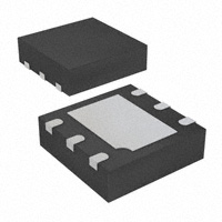
DFN6D (3x3 mm)
Internal protection circuitry includes thermal
protection with hysteresis and over current
limiting.
The ST1L02xx is especially suitable for data
storage applications such as HDDs, where can be
used to supply the read channel and memory
chips requiring 3.3 V.
The regulator is available in the small and thin
DFN6D (3x3 mm) package.
Description
The ST1L02xx is a low drop linear voltage
regulator capable to supply up to 1 A output
current.
The output voltage is fixed to 3.3 V, but under
customer request, it’s possible to have also 1.5 V,
1.8 V and 2.5 V. Thanks to the BiCMOS
technology, the quiescent current is well
controlled and maintained below 650 µA over the
whole allowed junction temperature range.
The ST1L02xx is stable with low ESR output
ceramic capacitors.
Table 1.
Device summary
Part numbers
Order codes
Package
ST1L02XX18
ST1L02PU18R
DFN6D (3x3 mm)
ST1L02XX25
ST1L02PU25R
DFN6D (3x3 mm)
ST1L02XX33
ST1L02PU33R
DFN6D (3x3 mm)
ST1L02XX
ST1L02PUR (1)
DFN6D (3x3 mm)
1. Only 3.3 V
March 2008
Rev 8
1/19
www.st.com
19
�ST1L02xx
Contents
1
Diagram . . . . . . . . . . . . . . . . . . . . . . . . . . . . . . . . . . . . . . . . . . . . . . . . . . . 3
2
Pin configuration . . . . . . . . . . . . . . . . . . . . . . . . . . . . . . . . . . . . . . . . . . . 4
3
Maximum ratings . . . . . . . . . . . . . . . . . . . . . . . . . . . . . . . . . . . . . . . . . . . . 5
4
Electrical characteristics . . . . . . . . . . . . . . . . . . . . . . . . . . . . . . . . . . . . . 6
5
Typical application . . . . . . . . . . . . . . . . . . . . . . . . . . . . . . . . . . . . . . . . . . 9
6
Typical characteristics . . . . . . . . . . . . . . . . . . . . . . . . . . . . . . . . . . . . . . 10
7
Package mechanical data . . . . . . . . . . . . . . . . . . . . . . . . . . . . . . . . . . . . 14
8
Revision history . . . . . . . . . . . . . . . . . . . . . . . . . . . . . . . . . . . . . . . . . . . 18
2/19
�ST1L02xx
Diagram
1
Diagram
Figure 1.
Schematic diagram
3/19
�Pin configuration
ST1L02xx
2
Pin configuration
Figure 2.
Pin connections (top through view)
ST1L02PXxx
ST1L02PX *
* Only 3.3 V.
Table 2.
Pin description
Pin n° for
ST1L02PXxx
Pin n° for
ST1L02PX
Symbol
1, 3
1, 4, 5
N.C.
Not connected.
2
6
GND
Ground. The exposed metallic pad of the package is connected to
GND.
4
2
VO
5
-
VO_SENSE
6
3
VI
4/19
Name and function
Output voltage pin. Bypass with a 4.7 µF capacitor to GND.
Sense output voltage pin. Must be connected to pin 4.
Supply voltage input pin. Bypass with a 4.7 µF capacitor to GND.
�ST1L02xx
Maximum ratings
3
Maximum ratings
Table 3.
Absolute maximum ratings
Symbol
Parameter
Value
Unit
VI
DC supply voltage
10
V
PTOT
Power dissipation
internally limited
W
Output current
internally limited
A
0 to 150
°C
-65 to 150
°C
260
°C
IO
TOP
Operating junction temperature range
TSTG
Storage temperature range (1)
TLEAD
Lead temperature (Soldering) 10 Sec.
1. Storage temperature >125 °C are acceptable only if the regulator is soldered to a PCBA.
Note:
Absolute maximum ratings are those values beyond which damage to the device may occur.
Functional operation under these condition is not implied.
Table 4.
Thermal data
Symbol
Parameter
Value
Unit
RthJC
Thermal resistance junction-case
10
°C/W
RthJA
Thermal resistance junction-ambient
55
°C/W
5/19
�Electrical characteristics
ST1L02xx
4
Electrical characteristics
Table 5.
Electrical characteristics for ST1L02XX18
(refer to the typical application schematic, VI = 4.5 V to 7 V, IO = 5 mA to 1 A, CI = 4.7 µF,
CO = 4.7 µF, TJ = 0 to 125 °C, unless otherwise specified). Typical values are intended at
TJ = 25 °C unless otherwise specified.
Symbol
Parameter
Test
Typ.
Max.
Unit
VO
Output voltage
VI = 4.75 V to 5.25 V, T=25°C
1.764
1.8
1.836
V
VO
Output voltage
VI = 4.75 V to 5.25 V
1.746
1.8
1.854
V
ΔVO
Line regulation
VI = 4.75 V to 5.25 V
15
mV
ΔVO
Load regulation
VI = 4.75 V, IO = 10 mA to 1 A
10
mV
Output current limit
VI = 5.5 V
IS
IOMIN
Dropout voltage (1)
IQ
Quiescent current
IQ
Quiescent current
Supply voltage rejection
(2)
mA
IO = 0.8 A
1.6
V
IO = 1 A
1.6
V
VI = 5 V, IO = 2 mA to 1 A, T = 25°C
500
µA
VI = 7 V, IO = 2 mA to 1 A
650
µA
VI = 5 ± 0.5 V, IO = 5 mA, f = 120 Hz
B = 10 Hz to 10 kHz, VI = 5 V,
IO = 5 mA
ΔVO/ΔIO
Load transient (rising) (3)
VI = 5 V, any 200 mA step from
100 mA to 1 A, tR ≥ 1 µs
ΔVO/ΔIO
Load transient (falling) (3)
ΔVO/ΔVI
Start-up transient (3)
ΔVO/ΔIO
Short circuit removal response
TSH
A
2
RMS Output noise (2)
eN
1.0
Minimum output current for
regulation
Vd
SVR
(3)
50
75
dB
0.003
%VO
5
%VO
VI = 5 V, IO = 1 A to 10 mA, tF ≥ 1 µs
3.6
V
VI =0 V to 5 V, IO = 10 mA to 1 A,
tR ≥ 1 µs
3.5
V
VI = 5 V, IO = short to 10 mA
3.5
V
Thermal shutdown trip point (3) VI = 5 V
1. See minimum start-up voltage, VI = 3.3 V.
2. Guaranteed by design. Not tested in production.
3. CI = 10 µF, CO = 10 µF, all X7R ceramic capacitors.
6/19
Min.
165
°C
�ST1L02xx
Table 6.
Electrical characteristics
Electrical characteristics for ST1L02XX25
(refer to the typical application schematic, VI = 4.5 V to 7 V, IO = 5 mA to 1 A, CI = 4.7 µF,
CO = 4.7 µF, TJ = 0 to 125 °C, unless otherwise specified). Typical values are intended at
TJ = 25 °C unless otherwise specified.
Symbol
Parameter
Test
Min.
Typ.
Max.
Unit
2.45
2.5
2.55
V
2.4375
2.5
2.5625
V
VO
Output voltage
VI = 4.75 V to 5.25 V, T = 25°C
VO
Output voltage
VI = 4.75 V to 5.25 V
ΔVO
Line regulation
VI = 4.75 V to 5.25 V
15
mV
ΔVO
Load regulation
VI = 4.75 V, IO = 10 mA to 1 A
10
mV
Output current limit
VI = 5.5 V
IS
IOMIN
Dropout voltage (1)
IQ
Quiescent current
IQ
Quiescent current
Supply voltage rejection
(2)
1.0
V
IO = 1 A
0.7
1.1
V
VI = 5 V, IO = 2 mA to 1 A, T= 25°C
500
µA
VI = 7 V, IO = 2 mA to 1 A
650
µA
VI = 5 ± 0.5 V, IO = 5 mA, f = 120 Hz
ΔVO/ΔIO
Load transient (rising) (3)
VI =5 V, any 200 mA step from
100mA to 1A, tR ≥ 1 µs
ΔVO/ΔIO
Load transient (falling) (3)
ΔVO/ΔVI
Start-up transient (3)
ΔVO/ΔIO
Short circuit removal response
TSH
mA
0.6
B = 10 Hz to 10 kHz, VI = 5V,
IO = 5 mA
(3)
2
IO = 0.8 A
RMS Output noise (2)
eN
A
Minimum output current for
regulation
Vd
SVR
1.0
50
75
dB
0.003
%VO
5
%VO
VI = 5 V, IO = 1 A to 10 mA, tF ≥ 1 µs
3.6
V
VI =0 V to 5 V, IO = 10 mA to 1 A,
tR ≥ 1 µs
3.5
V
VI = 5 V, IO = short to 10 mA
3.5
V
Thermal shutdown trip point (2) VI = 5 V
165
°C
1. See minimum start-up voltage, VI = 3.2 V.
2. Guaranteed by design. Not tested in production
3. CI = 10 µF, CO = 10 µF, all X7R ceramic capacitors.
7/19
�Electrical characteristics
Table 7.
ST1L02xx
Electrical characteristics for ST1L02XX33
(refer to the typical application schematic, VI = 4.5V to 7V, IO = 5mA to 1A, CI = 4.7µF,
CO = 4.7 µF, TJ = 0 to 125 °C, unless otherwise specified). Typical values are intended at
TJ = 25 °C unless otherwise specified.
Symbol
Parameter
Test
Min.
Typ.
Max.
Unit
VO
Output voltage
VI = 4.75 V to 5.25 V, T = 25°C
3.234
3.3
3.366
V
VO
Output voltage
VI = 4.75 V to 5.25 V
3.2175
3.3
3.3825
V
ΔVO
Line regulation
VI = 4.75 V to 5.25 V
15
mV
ΔVO
Load regulation
VI = 4.75 V, IO = 10 mA to 1 A
10
mV
Output current limit
VI = 5.5 V
IS
IOMIN
Dropout voltage
IQ
Quiescent current
IQ
Quiescent current
Supply voltage rejection
(2)
1.0
V
IO = 1 A
0.7
1.1
V
VI = 5 V, IO = 2 mA to 1 A, T= 25°C
500
µA
VI = 7 V, IO = 2 mA to 1 A
650
µA
VI = 5 ± 0.5V, IO = 5 mA, f = 120 Hz
ΔVO/ΔIO
Load transient (rising) (1)
VI = 5 V, any 200 mA step from
100 mA to 1 A, tR ≥ 1 µs
ΔVO/ΔIO
Load transient (falling) (1)
ΔVO/ΔVI
Start-up transient (1)
ΔVO/ΔIO
Short circuit removal response
TSH
50
75
dB
0.003
%VO
5
%VO
VI = 5 V, IO = 1 A to 10 mA, tF ≥ 1 µs
3.6
V
VI =0 V to 5 V, IO = 10 mA to 1 A,
tR ≥ 1 µs
3.5
V
VI = 5 V, IO = short to 10 mA
3.5
V
Thermal shutdown trip point (2) VI = 5 V
1. CI = 10 µF, CO = 10 µF, all X7R ceramic capacitors.
2. Guaranteed by design. Not tested in production.
8/19
mA
0.6
B = 10 Hz to 10 kHz, VI = 5 V,
IO = 5 mA
(1)
2
IO = 0.8 A
RMS Output noise (2)
eN
A
Minimum output current for
regulation
Vd
SVR
1.0
165
°C
�ST1L02xx
Typical application
5
Typical application
Figure 3.
Application schematic for ST1L02PM
Figure 4.
Application schematic for ST1L02PMxx
Note:
The regulator is designed to be stable with either tantalum and ceramic capacitors on the
input and the output. The expected values of the input and output ceramic capacitors are
from 1 µF to 22 µF with 4.7 µF typical. The input capacitor must be connected within 0.5
inches of the VI terminal. The output capacitor must also be connected within 0.5 inches of
output pin. There is no upper limit to the value of the input capacitor.
9/19
�Typical characteristics
ST1L02xx
6
Typical characteristics
Figure 5.
Output voltage vs temperature
Figure 6.
Line regulation vs temperature
Figure 7.
Line regulation vs temperature
Figure 8.
Load regulation vs temperature
Figure 9.
Dropout voltage vs temperature
Figure 10. Quiescent current vs temperature
10/19
�ST1L02xx
Typical characteristics
Figure 11. Quiescent current vs temperature
Figure 12. Quiescent current vs temperature
Figure 13. Quiescent current vs temperature
Figure 14. Quiescent current vs output current
Figure 15. Supply voltage rejection vs
temperature
Figure 16. Supply voltage rejection vs
frequency
11/19
�Typical characteristics
Figure 17. Output noise vs frequency
ST1L02xx
Figure 18. Change of VO with step load
change
VI=5V, IO=100mA to 300mA, CO=10μF, CI=10μF, tRISE≥1µs
Figure 19. Change of VO with step load
change
VI=5V, IO=300mA to 500mA, CO=10μF, CI=10μF, tRISE≥1µs
Figure 20. Change of VO with step load
change
VI=5V, IO=500mA to 700mA, CO=10μF, CI=10μF, tRISE≥1µs,
TJ=25°C
Figure 21. Change of VO with step load
change
Figure 22. Change of VO with step load
change
VI=5V, IO=700mA to 900mA, CO=10μF, CI=10μF, tRISE≥1µs,
TJ=25°C
VI=5V, IO=10mA to S.C., CO=10μF, CI=10μF, tRISE≥1µs,
TJ=25°C
12/19
�ST1L02xx
Typical characteristics
Figure 23. Line transient
VI = 4.75 V to 5.25 V, IO = 500 mA, CO=10 µF, CI = 2.2 µF,
tRISE ≥ 1 µs
13/19
�Package mechanical data
7
ST1L02xx
Package mechanical data
In order to meet environmental requirements, ST offers these devices in ECOPACK®
packages. These packages have a lead-free second level interconnect. The category of
second Level Interconnect is marked on the package and on the inner box label, in
compliance with JEDEC Standard JESD97. The maximum ratings related to soldering
conditions are also marked on the inner box label. ECOPACK is an ST trademark.
ECOPACK specifications are available at: www.st.com.
14/19
�ST1L02xx
Package mechanical data
DFN6D (3x3 mm) mechanical data
mm.
inch.
Dim.
Min.
A
0.80
A1
0
A3
0.02
Max.
Min.
1.00
0.031
0.05
0
0.20
b
0.23
D
2.90
D2
2.23
E
2.90
E2
1.50
e
L
Typ.
3.00
3.00
0.40
Max.
0.039
0.001
0.002
0.008
0.45
0.009
3.10
0.114
2.50
0.088
3.10
0.114
1.75
0.059
0.95
0.30
Typ.
0.018
0.118
0.122
0.098
0.118
0.122
0.069
0.037
0.50
0.012
0.016
0.020
7946637B
15/19
�Package mechanical data
ST1L02xx
Tape & Reel QFNxx/DFNxx (3x3) Mechanical Data
mm.
inch.
Dim.
Min.
Typ.
A
Min.
Typ.
330
13.2
Max.
12.992
C
12.8
D
20.2
0.795
N
60
2.362
T
16/19
Max.
0.504
0.519
18.4
0.724
Ao
3.3
0.130
Bo
3.3
0.130
Ko
1.1
0.043
Po
4
0.157
P
8
0.315
�ST1L02xx
Package mechanical data
Figure 24. DFN6 (3x3 mm) footprint recommended data
17/19
�Revision history
ST1L02xx
8
Revision history
Table 8.
Document revision history
Date
Revision
25-Feb-2005
1
First release.
10-Jan-2006
2
Add new order codes and tables of the electrical characteristics.
16-May-2006
3
General feature has been updated and add note 3 in table 6.
05-Jul-2006
4
Updated mechanical data DFN6 (3x3).
22-Feb-2007
5
Add note in Figure 2 and in order codes.
03-Apr-2007
6
Add order codes and mechanical data DFN6D.
05-Sep-2007
7
Add Table 1 in cover page.
12-Mar-2008
8
Removed: mechanical data DFN6.
18/19
Changes
�ST1L02xx
Please Read Carefully:
Information in this document is provided solely in connection with ST products. STMicroelectronics NV and its subsidiaries (“ST”) reserve the
right to make changes, corrections, modifications or improvements, to this document, and the products and services described herein at any
time, without notice.
All ST products are sold pursuant to ST’s terms and conditions of sale.
Purchasers are solely responsible for the choice, selection and use of the ST products and services described herein, and ST assumes no
liability whatsoever relating to the choice, selection or use of the ST products and services described herein.
No license, express or implied, by estoppel or otherwise, to any intellectual property rights is granted under this document. If any part of this
document refers to any third party products or services it shall not be deemed a license grant by ST for the use of such third party products
or services, or any intellectual property contained therein or considered as a warranty covering the use in any manner whatsoever of such
third party products or services or any intellectual property contained therein.
UNLESS OTHERWISE SET FORTH IN ST’S TERMS AND CONDITIONS OF SALE ST DISCLAIMS ANY EXPRESS OR IMPLIED
WARRANTY WITH RESPECT TO THE USE AND/OR SALE OF ST PRODUCTS INCLUDING WITHOUT LIMITATION IMPLIED
WARRANTIES OF MERCHANTABILITY, FITNESS FOR A PARTICULAR PURPOSE (AND THEIR EQUIVALENTS UNDER THE LAWS
OF ANY JURISDICTION), OR INFRINGEMENT OF ANY PATENT, COPYRIGHT OR OTHER INTELLECTUAL PROPERTY RIGHT.
UNLESS EXPRESSLY APPROVED IN WRITING BY AN AUTHORIZED ST REPRESENTATIVE, ST PRODUCTS ARE NOT
RECOMMENDED, AUTHORIZED OR WARRANTED FOR USE IN MILITARY, AIR CRAFT, SPACE, LIFE SAVING, OR LIFE SUSTAINING
APPLICATIONS, NOR IN PRODUCTS OR SYSTEMS WHERE FAILURE OR MALFUNCTION MAY RESULT IN PERSONAL INJURY,
DEATH, OR SEVERE PROPERTY OR ENVIRONMENTAL DAMAGE. ST PRODUCTS WHICH ARE NOT SPECIFIED AS "AUTOMOTIVE
GRADE" MAY ONLY BE USED IN AUTOMOTIVE APPLICATIONS AT USER’S OWN RISK.
Resale of ST products with provisions different from the statements and/or technical features set forth in this document shall immediately void
any warranty granted by ST for the ST product or service described herein and shall not create or extend in any manner whatsoever, any
liability of ST.
ST and the ST logo are trademarks or registered trademarks of ST in various countries.
Information in this document supersedes and replaces all information previously supplied.
The ST logo is a registered trademark of STMicroelectronics. All other names are the property of their respective owners.
© 2008 STMicroelectronics - All rights reserved
STMicroelectronics group of companies
Australia - Belgium - Brazil - Canada - China - Czech Republic - Finland - France - Germany - Hong Kong - India - Israel - Italy - Japan Malaysia - Malta - Morocco - Singapore - Spain - Sweden - Switzerland - United Kingdom - United States of America
www.st.com
19/19
�


 工商网监
湘ICP备2023018690号
工商网监
湘ICP备2023018690号
