ST2378E
8-bit dual supply 1.71 V to 5.5 V level translator
with I/O VCC ±15 kV ESD protection
Datasheet - production data
Description
Flip-Chip20
The ST2378E device is an 8-bit, dual supply,
bidirectional level translator with ±15 kV ESD
protection on I/Os at VCC side. It is designed to
interface data transfer between low voltage
ASICs/PLDs and higher voltage systems.
Externally applied voltage, VCC and VL, set logic
levels at both sides with the range specified as
1.71 V VL 5.5 V and VL VCC 5.5 V.
For proper operation, VCC should be set higher
than VL.
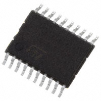
TSSOP20
Features
High speed
– tPD = 15 ns (max.) at TA = 85 °C
– VL = 1.8 V
– VCC = 5.5 V
Guaranteed data rate
– 13 Mbps (1.8 V VL VCC 5.5 V)
Low power dissipation
– ITS-VL = ITS-VCC = 1 A (max.) at TA = 85 °C
– IQVL = 100 A (max.) at TA = 85 °C
– IQCC = 10 A (max.) at TA = 85 °C
Output impedance
– |IOHA| = 20 A (min.) at VL = 1.8 V; VCC = 5.5 V
– IOLA = 1.0 A (min.) at VL = 1.8 V; VCC = 5.5 V
Utilizing a transmission-gate-based design, this
device allows bidirectional asynchronous data
transfer, which means each channel is allowed to
have either VCC to VL or VL to VCC data transfer
direction independently and no direction pin is
required. The ST2378E device operates at a
guaranteed data rate of 13 Mbps over the entire
specified operating voltage range.
Among the other features, the OE pin allows
disable mode operation whereby current
consumption is reduced to less than 1 μA.
Table 1. Device summary
Part number
Temp.
range (°C)
Package
Marking
Bidirectional level translation
ST2378EBJR
-40 to 85
Flip-Chip20 ST2378E
Totem pole and open drain driving for I2C
communications
ST2378ETTR
-40 to 85
TSSOP20
ST2378E
5 V tolerant on enable pin
Wide operating voltage range
– VL (opr.) = 1.71 V to VCC
– VCC (opr.) = 1.71 V to 5.5 V
ESD performance
HBM > 15 kV ESD protection on I/O VCC lines
Lead-free Flip-Chip and TSSOP package
May 2015
This is information on a product in full production.
DocID009489 Rev 3
1/20
www.st.com
�Contents
ST2378E
Contents
1
Block diagram . . . . . . . . . . . . . . . . . . . . . . . . . . . . . . . . . . . . . . . . . . . . . . 3
2
Pin settings . . . . . . . . . . . . . . . . . . . . . . . . . . . . . . . . . . . . . . . . . . . . . . . . 4
3
2.1
Pin connection . . . . . . . . . . . . . . . . . . . . . . . . . . . . . . . . . . . . . . . . . . . . . . 4
2.2
Pin description . . . . . . . . . . . . . . . . . . . . . . . . . . . . . . . . . . . . . . . . . . . . . . 4
Electrical data . . . . . . . . . . . . . . . . . . . . . . . . . . . . . . . . . . . . . . . . . . . . . . 5
3.1
Maximum ratings . . . . . . . . . . . . . . . . . . . . . . . . . . . . . . . . . . . . . . . . . . . . 5
3.2
Recommended operating conditions . . . . . . . . . . . . . . . . . . . . . . . . . . . . . 5
4
Electrical characteristics . . . . . . . . . . . . . . . . . . . . . . . . . . . . . . . . . . . . . 6
5
Test circuit . . . . . . . . . . . . . . . . . . . . . . . . . . . . . . . . . . . . . . . . . . . . . . . . 11
6
Waveforms . . . . . . . . . . . . . . . . . . . . . . . . . . . . . . . . . . . . . . . . . . . . . . . . 12
7
Package information . . . . . . . . . . . . . . . . . . . . . . . . . . . . . . . . . . . . . . . . 14
8
2/20
7.1
TSSOP20 package information . . . . . . . . . . . . . . . . . . . . . . . . . . . . . . . . 15
7.2
TSSOP20 packing information . . . . . . . . . . . . . . . . . . . . . . . . . . . . . . . . . 16
7.3
Flip-Chip20 package information . . . . . . . . . . . . . . . . . . . . . . . . . . . . . . . 17
7.4
Flip-Chip20 packing information . . . . . . . . . . . . . . . . . . . . . . . . . . . . . . . . 18
Revision history . . . . . . . . . . . . . . . . . . . . . . . . . . . . . . . . . . . . . . . . . . . 19
DocID009489 Rev 3
�ST2378E
1
Block diagram
Block diagram
Figure 1. Block diagram
Figure 2. Functional diagram (1 I/O line)
DocID009489 Rev 3
3/20
20
�Pin settings
ST2378E
2
Pin settings
2.1
Pin connection
Figure 3. Pin connection
Flip-Chip20
(bottom view) bump side
2.2
TSSOP20 (top view)
Pin description
Table 2. Pin description
4/20
Flip-Chip20 pin N°
TSSOP20 pin N°
Symbol
Name and function
E2, D1, D2, C1, C2, B1,
B2, A1
2, 18, 4, 16, 6, 14, 8, 12
I/OVL1 to I/OVL8
Data inputs/outputs
E3, D4, D3, C4, C3, B4,
B3, A4
19, 3, 17, 5, 15, 7, 13, 9 I/OVCC1 to I/OVCC8
Data inputs/outputs
A2
11
OE
Output enable inputs
A3
10
GND
Ground (0 V)
E1
1
VL
Positive supply voltage
E4
20
VCC
Positive supply voltage
DocID009489 Rev 3
�ST2378E
Electrical data
3
Electrical data
3.1
Maximum ratings
Table 3. Absolute maximum rating
Symbol
Parameter
Value
Unit
VL
Supply voltage
-0.3 to VCC
V
VCC
Supply voltage
-0.3 to +7.0
V
VOE
DC control input voltage
-0.3 to +7.0
V
-0.3 to VL + 0.3
V
-0.3 to VCC + 0.3
V
DC input diode current (OE control pin)
20
mA
IIOVL
DC output current
25
mA
IIOVCC
DC output current
25
mA
Continuous
mA
100
mA
VI/OVL
VI/OVCC
IIK
ISCTOUT
ICCB
DC I/OVL input voltage (OE = GND or VL)
DC I/OVCC input voltage (OE = GND or VL)
Short-circuit duration I/OVL, I/OVCC driven from 40 mA
source
DC VCC or ground current
Pd
Power dissipation(1)
500
mW
Tstg
Storage temperature
-65 to +150
°C
TL
Lead temperature (10 sec.)
300
°C
Value
Unit
1. 500 mW: 65 °C derated to 300 mW by 10 mW/°C: 65 °C to 85 °C.
3.2
Recommended operating conditions
Table 4. Recommended operating conditions
Symbol
Parameter
VL
Supply voltage
1.71 to VCC
V
VCC
Supply voltage
1.71 to 5.5
V
Input voltage (OE output enable pin, VL power supply
referred)
0 to 5.5
V
I/OVL voltage
0 to VL
V
I/OVCC voltage
0 to VCC
V
Operating temperature
-40 to 85
°C
0 to 10
ns/V
1.71 < VL < VCC < 5 V
0 to 10
ns/V
VCC = VL = 5 V
0 to 3
ns/V
VI
VI/OVL
VI/OVCC
Top
dt/dv
Input rise and fall time (OE control pin)(1)
dt/dv
Input rise and fall time(2)
1. VOE from 10% VL to 90% VL.
2. VIOVL from 10%VL to 90%VL; VIOVCC from 10% VCC to 90% VCC.
DocID009489 Rev 3
5/20
20
�Electrical characteristics
4
ST2378E
Electrical characteristics
Table 5. DC specification
Test condition(1)
Symbol Parameter
VIHL
VILL
VIHC
VILC
VIH-TS
VIL-TS
VOHL
VOLL
6/20
High level
input
voltage
(I/OVL)
Low level
input
voltage
(I/OVL)
High level
input
voltage
(I/OVCC)
Low level
input
voltage
(I/OVCC)
High level
input
voltage
(OE)
Low level
input
voltage
(OE)
High level
output
voltage
I/OVL
Low level
output
voltage
I/OVL
Value
TA = 25 °C
VL (V)(2) VCC (V)(2)
Min.
Typ.(3)
-40 to 85 °C
Max.
Min.
Max.
1.8
VL to 5.5
VL-0.2
VL-0.2
2.5
VL to 5.5
0.75 VL
0.75 VL
3.3
VL to 5.5
0.75 VL
0.75 VL
5.0
VL to 5.5
0.75 VL
0.75 VL
1.8
VL to 5.5
0.15
0.15
2.5
VL to 5.5
0.30
0.30
3.3
VL to 5.5
0.30
0.30
5.0
VL to 5.5
0.30
0.30
1.8
VL to 5.5
VL-0.2
VL-0.2
2.5
VL to 5.5
0.75 VCC
0.75 VCC
3.3
VL to 5.5
0.75 VCC
0.75 VCC
5.0
VL to 5.5
0.75 VCC
0.75 VCC
1.8
VL to 5.5
0.15
0.15
2.5
VL to 5.5
0.30
0.30
3.3
VL to 5.5
0.30
0.30
5.0
VL to 5.5
0.30
0.30
1.8
VL to 5.5
VL-0.2
VL-0.2
2.5
VL to 5.5
0.75 VL
0.75 VL
3.3
VL to 5.5
0.75 VL
0.75 VL
5.0
VL to 5.5
0.75 VL
0.75 VL
1.8
VL to 5.5
0.15
0.15
2.5
VL to 5.5
0.25 VL
0.25
VL
3.3
VL to 5.5
0.25 VL
0.25
VL
5.0
VL to 5.5
0.25 VL
0.25
VL
IO = -20 A
0.67 VL
I/OVCC VCC -0.2
1.8 to
5.5
Unit
V
V
V
V
V
V
0.67 VL
VL to 5.5
V
IO = 1.0 mA
I/OVCC 0.15 V
DocID009489 Rev 3
0.40
0.40
�ST2378E
Electrical characteristics
Table 5. DC specification (continued)
Test condition(1)
Symbol Parameter
VOHC
High level
output
voltage
I/OVCC
VOLC
Low level
output
voltage
I/OVCC
ITSL
Control
input
leakage
current
(OE)
High
impedance
input
ITS-LKG leakage
current
(IOVL,
I/OVCC)
IQVCC
IQVL
ITS-VL
TA = 25 °C
VL (V)(2) VCC (V)(2)
Min.
IO = -20 A
I/OVL VL -0.2
1.8 to
5.5
Value
Typ.(3)
-40 to 85 °C
Max.
Min.
Unit
Max.
0.67 VCC
0.67 VCC
VL to 5.5
V
IO = 1.0 mA
I/OVL 0.15 V
0.40
0.40
1.8 to
5.5
VL to 5.5 VI = GND or 5.5
1
1
A
1.8 to
5.5
VL to 5.5 OE = GND
1
1
A
Quiescent
1.8 to
supply
5.5
current VCC
VL to 5.5
I/OVL, I/OVCC
unconnected
0.1
1
10
A
Quiescent
supply
current VL
VL to 5.5
I/OVL, I/OVCC
unconnected
13
20
100
A
VL to 5.5
OE = GND
I/OVL= GND to VL
I/OVCC = GND to
VCC
1
1
A
1.8 to
5.5
High
impedance
mode
1.8 to
quiescent 5.5
supply
current VL
1. For normal operation, ensure VL < (VCC + 0.3 V). During power-up, VL > (VCC + 0.3 V) will not damage the device.
2. Power supply range: VL, VCC 1.8 V ± 5%, 2.5 ± 0.2 V, 3.3 ± 0.3 V, 5.0 ± 0.5 V.
3. Typical values are referred to TA = 25 °C.
DocID009489 Rev 3
7/20
20
�Electrical characteristics
ST2378E
Table 6. AC electrical characteristics (totem pole driving)
Symbol
tRVCC
tFVCC
tRVL
tFVL
Parameter
Rise time
I/OVCC(5)
Fall time I/OVCC(5)
Rise time
I/OVL(5)
Fall time I/OVL
(5)
tPLH
tIOVL-VCC
Propagation delay time(6)
I/OVL-LH to I/OVCC-LH
I/OVL-HL to I/OVCC-HL
tPHL
8/20
Test condition(1)
Value
CL= 15 pF, tr = tf 6 ns(2)
Driver output
RT50
-40 to +85 °C
VL (V)(3)
VCC (V)(3)
1.8
Unit
Typ.(4)
Max.
1.8
11
15
1.8
2.5
11
15
1.8
3.3
10
15
1.8
5.0
9
15
2.5
3.3
8
15
1.8
1.8
6
15
1.8
2.5
7
15
1.8
3.3
8
15
1.8
5.0
10
15
2.5
3.3
6
15
1.8
1.8
12
15
1.8
2.5
10
15
1.8
3.3
9
15
1.8
5.0
10
15
2.5
3.3
7
15
1.8
1.8
7
15
1.8
2.5
6
15
1.8
3.3
6
15
1.8
5.0
7
15
2.5
3.3
4
15
1.8
1.8
6
15
1.8
2.5
7
15
1.8
3.3
7
15
1.8
5.0
7
15
2.5
3.3
4
15
1.8
1.8
5
15
1.8
2.5
5
15
1.8
3.3
6
15
1.8
5.0
8
15
2.5
3.3
4
15
DocID009489 Rev 3
Min.
ns
ns
ns
ns
ns
�ST2378E
Electrical characteristics
Table 6. AC electrical characteristics (totem pole driving) (continued)
Symbol
Parameter
tPLH
tIOVCC-VL
Propagation delay time(6)
I/OVCC-LH to I/OVL-LH
I/OVCC-HL to I/OVL-HL
tPHL
tPZL tPZH
tPLZ tPZL
tOSLH
tOSHL
DR
Output enable and disable time
Channel to channel skew time(7),(8)
Maximum data rate
Test condition(1)
Value
CL = 15 pF, tr = tf 6
ns(2) Driver output
RT50
-40 to +85 °C
VL (V)(3)
VCC (V)(3)
1.8
Unit
Typ.(4)
Max.
1.8
2
15
1.8
2.5
2
15
1.8
3.3
2
15
1.8
5.0
2
15
2.5
3.3
2
15
1.8
1.8
5
15
1.8
2.5
5
15
1.8
3.3
5
15
1.8
5.0
6
15
2.5
3.3
4
15
1.8
1.8
60
80
1.8
5.0
150
200
1.8
1.8
0.1
1
1.8
5.0
0.5
1
1.8 to 5.0
VL to 5.0
Min.
13
ns
ns
ns
Mbps
1. For normal operation, ensure VL < (VCC + 0.3 V). During power-up, VL > (VCC + 0.3 V) will not damage the device.
2. For VCC = VL = 1.8 V, tr = tf 4 ns.
3. Power supply range: VL, VCC 1.8 V ± 5%, 2.5 ± 0.2 V, 3.3 ± 0.3 V, 5.0 ± 0.5 V.
4. Typical values are referred to TA = 25 °C.
5. Rise time: 10% to 90%, fall time 90% to 10%.
6. Propagation delay time: 50% to 50%.
7. Skew is defined as the absolute value of the difference between the actual propagation delay for any two outputs of the
same device switching in the same direction, either HIGH or LOW (tOSLH = | tPLHm - tPLHn|, tOSHL = | tPHLm - tPHLn|.
8.
Each translator equally loaded; parameter guaranteed by design.
DocID009489 Rev 3
9/20
20
�Electrical characteristics
ST2378E
Table 7. AC characteristic (open drain driving)
Symbol
Parameter
tRVCC
Rise time I/OVCC(5)
tFVCC
Fall time I/OVCC(5)
tRVL
Rise time I/OVL(5)
tFVL
Fall time I/OVL(5)
tIOVL-VCC
tIOVCC-VL
tPZL tPZH
tPLZ tPZL
tOSLH
tOSHL
DR
Propagation delay time(6)
I/OVL-LH to I/OVCC-LH
I/OVL-HL to I/OVCC-HL
Propagation delay time(6)
I/OVCC-LH to I/OVL-LH
I/OVCC-HL to I/OVL-HL
tPLH
tPHL
tPLH
tPHL
Output enable and disable time
Channel to channel skew time(7),(8)
Maximum data rate
Test condition(1)
Value
CL = 15 pF, tr = tf 6
ns(2) Driver output
RT 50
-40 to +85 °C
VL (V)(3)
VCC (V)(3)
1.8
Unit
Typ.(4)
Max.
1.8
210
300
1.8
5.0
59
150
1.8
1.8
12
30
1.8
5.0
20
30
1.8
1.8
210
300
1.8
5.0
96
150
1.8
1.8
11
30
1.8
5.0
11
30
1.8
1.8
210
300
1.8
5.0
100
150
1.8
1.8
7
20
1.8
5.0
14
20
1.8
1.8
210
300
1.8
5.0
57
150
1.8
1.8
7
20
1.8
5.0
8
20
1.8
1.8
60
80
1.8
5.0
150
200
1.8
1.8
10
20
1.8
5.0
2
10
1.8 to 5.0
VL to 5.0
Min.
800
ns
ns
ns
ns
ns
ns
ns
ns
kbps
1. For normal operation, ensure VL < (VCC + 0.3 V). During power-up, VL > (VCC + 0.3 V) will not damage the device.
2. For VCC = VL = 1.8 V, tr = tf 4 ns.
3. Power supply range: VL, VCC 1.8 V ± 5%, 2.5 ± 0.2 V, 3.3 ± 0.3 V, 5.0 ± 0.5 V.
4. Typical values are referred to TA = 25 °C.
5. Rise time:10% to 90%, fall time 90% to 10%.
6. Propagation delay time: 50% to 50%.
7.
Skew is defined as the absolute value of the difference between the actual propagation delay for any two outputs of the
same device switching in the same direction, either HIGH or LOW (tOSLH = | tPLHm - tPLHn|, tOSHL = | tPHLm - tPHLn|.
8. Each translator equally loaded; parameter guaranteed by design.
10/20
DocID009489 Rev 3
�ST2378E
5
Test circuit
Test circuit
Figure 4. Test circuit
Table 8. Test circuit switches
Switch
Test
Note:
Driving I/OVL
Driving I/OVCC
Open drain driving
tPLH, tPHL
Open
Open
Open
tPZL, tPLZ
VCC
VL
-
tPZH, tPHZ
GND
GND
-
CL = 15/50 pF or equivalent (includes jig and probe capacitance).
R1 = 1 kΩ or equivalent.
RT = ZOUT of pulse generator (typically 50 Ω ).
Table 9. Truth table
Control pin
1.
Bidirectional input/outputs
OE
I/OVL
I/OVCC
H(1)
H(1)
H(2)
H(1)
L
L
L
Z
Z
High level VL power supply referred.
2. High level VCC power supply referred.
Note:
X = do not care; Z = high impedance.
DocID009489 Rev 3
11/20
20
�Waveforms
6
ST2378E
Waveforms
Table 10. Waveform symbol value
Driving I/OVL
Driving I/OVCC
Symbol
1.8 V VLVCC 2.5
V
3.3 V VLVCC 5.0
V
1.8 V VLVCC 2.5
V
3.3 V VLVCC 5.0
V
VIH
VL
VL
VCC
VCC
VIM
50% VL
50% VL
50% VCC
50% VCC
VOM
50% VCC
50% VCC
50% VCC
50% VCC
VX
VOL +0.15 V
VOL +0.3 V
VOL +0.15 V
VOL +0.3 V
VY
VOH -0.15 V
VOH -0.3 V
VOH -0.15 V
VOH -0.3 V
Figure 5. Waveform - propagation delay (f = 1 MHz; 50% duty cycle)
12/20
DocID009489 Rev 3
�ST2378E
Waveforms
Figure 6. Waveform - output enable and disable time (f = 1 MHz; 50% duty cycle)
DocID009489 Rev 3
13/20
20
�Package information
7
ST2378E
Package information
In order to meet environmental requirements, ST offers these devices in different grades of
ECOPACK® packages, depending on their level of environmental compliance. ECOPACK
specifications, grade definitions and product status are available at: www.st.com.
ECOPACK is an ST trademark.
14/20
DocID009489 Rev 3
�ST2378E
7.1
Package information
TSSOP20 package information
Figure 7. TSSOP20 package outline
Table 11. TSSOP20 package mechanical data
Dimensions
Symbol
mm
Min.
Typ.
A
inch
Max.
Min.
Typ.
1.2
A1
0.05
A2
0.8
b
Max.
0.047
0.15
0.002
0.004
0.006
1.05
0.031
0.039
0.041
0.19
0.30
0.007
0.012
c
0.09
0.20
0.004
0.0079
D
6.4
6.5
6.6
0.252
0.256
0.260
E
6.2
6.4
6.6
0.244
0.252
0.260
E1
4.3
4.4
4.48
0.169
0.173
0.176
e
1
0.0256
BSC
0.65 BSC
K
0°
L
0.45
0.60
8°
0°
0.75
0.018
DocID009489 Rev 3
8°
0.024
0.030
15/20
20
�Package information
7.2
ST2378E
TSSOP20 packing information
Figure 8. TSSOP20 tape and reel outline
1. Drawing not to scale.
Table 12. TSSOP20 tape and reel mechanical data
Dimensions
Symbol
mm
Min.
A
Max.
Min.
330
13.2
Typ.
Max.
12.992
C
12.8
D
20.2
0.795
N
60
2.362
T
16/20
Typ.
inch
0.504
22.4
0.519
0.882
Ao
6.8
7
0.268
0.276
Bo
6.9
7.1
0.272
0.280
Ko
1.7
1.9
0.067
0.075
Po
3.9
4.1
0.153
0.161
P
11.9
12.1
0.468
0.476
DocID009489 Rev 3
�ST2378E
7.3
Package information
Flip-Chip20 package information
Figure 9. Flip-Chip20 package outline
Table 13. Flip-Chip20 package mechanical data
Dimensions
Symbol
mm
mils
Min.
Typ.
Max.
Min.
Typ.
Max.
A
0.81
0.89
1.00
31.9
35.0
39.4
A1
0.15
0.24
0.35
5.9
9.4
13.8
A2
0.65
25.6
b
0.25
0.30
0.35
9.8
11.8
13.8
D
2.41
2.46
2.51
94.9
96.9
98.8
D1
E
2.00
1.93
1.98
78.7
2.03
76.0
78.0
E1
1.5
59.1
e
0.50
19.7
SE
0.25
9.8
DocID009489 Rev 3
79.9
17/20
20
�Package information
7.4
ST2378E
Flip-Chip20 packing information
Figure 10. Flip-Chip20 tape and reel outline
1. Drawing not to scale.
Table 14. Flip-Chip20 tape and reel mechanical data
Dimensions
Symbol
mm
Min.
Typ.
A
Max.
Min.
Typ.
180
13.2
Max.
7.086
C
12.8
D
20.2
0.795
N
60
2.362
T
18/20
inch
0.504
0.519
14.4
0.567
Ao
2.13
2.23
2.33
0.084
0.088
0.092
Bo
2.62
2.72
2.82
0.103
0.107
0.111
Ko
1.05
1.15
1.25
0.041
0.045
0.049
Po
3.9
4.1
0.153
0.161
P
3.9
4.1
0.153
0.161
DocID009489 Rev 3
�ST2378E
8
Revision history
Revision history
Table 15. Document revision history
Date
Revision
Changes
10-Apr-2006
1
Initial release.
18-Sep-2012
2
Updated Figure 2 (added resistor values).
Updated notes and cross-references of the notes below Table 5 to
Table 7, replaced tFCC by tFVCC in Table 6 and Table 7.
Updated ECOPACK text in Section 7., reformatted Section 7 (added
Table 11 to Table 14, moved note below Figure 8 and Figure 10).
Minor corrections throughout document.
18-May-2015
3
Added Table 1: Device summary.
Revised presentation of Section 7: Package information.
Minor textual updates.
DocID009489 Rev 3
19/20
20
�ST2378E
IMPORTANT NOTICE – PLEASE READ CAREFULLY
STMicroelectronics NV and its subsidiaries (“ST”) reserve the right to make changes, corrections, enhancements, modifications, and
improvements to ST products and/or to this document at any time without notice. Purchasers should obtain the latest relevant information on
ST products before placing orders. ST products are sold pursuant to ST’s terms and conditions of sale in place at the time of order
acknowledgement.
Purchasers are solely responsible for the choice, selection, and use of ST products and ST assumes no liability for application assistance or
the design of Purchasers’ products.
No license, express or implied, to any intellectual property right is granted by ST herein.
Resale of ST products with provisions different from the information set forth herein shall void any warranty granted by ST for such product.
ST and the ST logo are trademarks of ST. All other product or service names are the property of their respective owners.
Information in this document supersedes and replaces information previously supplied in any prior versions of this document.
© 2015 STMicroelectronics – All rights reserved
20/20
DocID009489 Rev 3
�