AS3980
UHF RFID Single Chip Reader EPC
Class1 Gen2
General Description
The AS3980 is an UHF RFID reader IC enabling battery-powered,
small form-factor handheld and embedded UHF reader systems
for a single tag environment of EPC Class1 Gen2 compliant UHF
RFID tags. The device directly supports ISO 18000-6C/ EPC
Class1 Gen2 transponders in a single-tag environment. The
AS3980 operates at very low power, which means that this
advanced RFID reader IC is suitable for use in portable and
battery-powered equipment such as mobile phones. AS3980
requires only an external simple 8-bit μC to create a complete
RFID reader system. AS3980 is highly integrated and
implements the RFID functions on chip thus eliminating a need
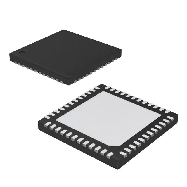
for a complex RFID co-processor. Packaged in a 7 x 7 mm QFN
outline, the IC benefits from fabrication process technology
unique to ams to deliver very high sensitivity and providing
high immunity to the effects of antenna reflections and
self-jamming. This is critical in mobile and embedded
applications, in which antenna design is often compromised by
cost or size constraints. High sensitivity enables end-product
designs to achieve their required read range while using a
simpler and cheaper antenna, thus reducing system
bill-of-materials cost.
Ordering Information and Content Guide appear at end of
datasheet.
Key Benefits & Features
The benefits and features of AS3980, UHF RFID Single Chip
Reader EPC Class1 Gen2 are listed below:
Figure 1:
Added Value of Using AS3980
Benefit
Optimized for battery operation
ISO 18000-6C implemented in HW.
Feature
• Supply voltage range 3.0V to 3.6V
• Limited operation possible down to 2.7V
• Peripheral I/O supply range: 1.65V to 5.5V
Low coding effort and MCU requirements
• Basic protocol support for ISO 18000-6C (EPC Class1 Gen2)
• Reception mode M8 on 40kHz link frequency
High PSRR
• Integrated supply regulators
Flexible modulation method
• ASK or PR-ASK modulation
Small package footprint – saving PCB area
• 48-pin QFN (7x7x0.9 mm) package
ams Short Datasheet
[v1-00] 2015-Jul-03
Page 1
Document Feedback
�AS3980 − General Description
Benefit
Feature
Avoidance of communication holes
• Automatic I/Q selection
Tag movement detection support
• Phase bit for tag tracking with 8-bit linear RSSI
Wide temperature range
• -40ºC to 85ºC
Applications
The AS3980 device is well suited for:
• Embedded consumer/industrial applications with cost
constraints such as beverage dispensing.
• Hand-Held readers.
• Mobile UHF RFID readers.
• Battery-Powered stationary readers.
• FMCG and brand protection
• Product authentication
Block Diagram
The functional blocks of this device for reference are
shown below:
Figure 2:
AS3980 Block Diagram
AS3980
Analog Front-End
IQ
Mixer
Gain
Amplifiers
RX
Filter
Digitizer
I
MIXS_IN
IRQ
Q
EN
RSSI
RFOPX
PA
0 dBm
Balu
n
I
Q
Shaping
RFONX
OSCI
TCXO
20 MHz
Oscillato
r&
Timing
System
Page 2
Document Feedback
SPI
SCLK
MOSI
MISO
NCS
Protocol & Logic
VCO /
PLL
TX Framing
OSCO
+3.3 V
Supply
Regulators and
References
MCU
Interface
Serial Conversion
and
CRC Parity Check
RX
Decoder Bit
Framing
DUAL 24
Byte FIFO
Registers
ams Short Datasheet
[v1-00] 2015-Jul-03
�AS3980 − Pin Assignment
The AS3980 pin assignments are described below.
Pin Assignment
Figure 3:
Pin Diagram
COMN_A
COMP_A
VDD_LF
LF_CEXT
VDD_A
VOSC
AGD
CD1
CD2
ADC
VDD_IO
SCLK
48
47
46
45
44
43
42
41
40
39
38
37
AS3980 Pin Assignment: This figure
shows the pin assignment and location
viewed from top.
COMP_B
1
36
CLSYS
COMN_B
2
35
MOSI
VDD_LFI
3
34
MISO
NC
4
33
NCS
MIXS_IN
5
32
IRQ
NC
6
31
EN
VDD_TXPAB
7
30
OSCO
CBV
8
29
OSCI
CBIB
9
28
VDD_D
VDD_MIX
10
27
OAD
VEXT
11
26
OAD2
VDD_B
12
25
VSN
AS3980
15
16
17
18
19
20
21
22
23
VSN
NC
NC
VSN
VSN
NC
NC
VSN
RFONX
24
14
RFOPX
13
VDD_RF
VEXT_RF
49 (exposed pad)
Figure 4:
Pin Description
Pin Number
Pin Name
Pin Type
Description
48-Pin QFN
1
COMP_B
Analog I/O
Internal node, connect de-coupling capacitor to VDD_LFI
2
COMN_B
Analog I/O
Internal node, connect de-coupling capacitor to VDD_LFI
3
VDD_LFI
Supply pad
Positive supply for LF input stage, connect to VDD_MIX
4
NC
5
MIXS_IN
6
NC
7
VDD_TXPAB
Supply pad
Bias positive supply. Connect to VDD_MIX
8
CBV
Analog I/O
Internal node, connect de-coupling capacitor to VDD_MIX
9
CBIB
Analog I/O
Internal node, connect de-coupling capacitor to ground
10
VDD_MIX
Analog I/O
Mixer positive supply, internally regulated
ams Short Datasheet
[v1-00] 2015-Jul-03
Not connected
Analog input
Single ended mixer input
Not connected
Page 3
Document Feedback
�AS3980 − Pin Assignment
Pin Number
Pin Name
Pin Type
Description
48-Pin QFN
11
VEXT
Supply pad
Main positive supply input, input to regulators
12
VDD_B
Analog I/O
Buffer positive supply, internally regulated
13
VDD_RF
Analog I/O
RF positive supply, internally regulated
14
VEXT_RF
Supply pad
RF positive supply regulator input
15
VSN
Supply pad
Negative supply
16
NC
Not connected
17
NC
Not connected
18
VSN
Supply pad
Negative supply
19
VSN
Supply pad
Negative supply
20
NC
Not connected
21
NC
Not connected
22
VSN
23
Supply pad
Negative supply
RFONX
Analog output
Low power linear negative RF output (~0dBm)
24
RFOPX
Analog output
Low power linear positive RF output (~0dBm)
25
VSN
Supply pad
Negative supply
26
OAD2
Analog I/O
Analog or digital received signal output
27
OAD
Analog I/O
Analog or digital received signal output
28
VDD_D
Analog I/O
Positive supply for logic, internally regulated
29
OSCI
Analog input
Crystal oscillator input or short to ground in case external
TCXO is used
30
OSCO
Analog I/O
Crystal oscillator output or external 20MHz clock input
31
EN
Digital input
Enable input
32
IRQ
Digital output
Interrupt request output
33
NCS
Digital input
Serial Peripheral Interface Enable (active low)
34
MISO
Digital output
/ tri-state
Serial Peripheral Interface DATA output
35
MOSI
Digital input
Serial Peripheral Interface DATA input
36
CLSYS
Digital output
Clock Output for MCU
37
SCLK
Digital input
Serial Peripheral Interface Clock
Page 4
Document Feedback
ams Short Datasheet
[v1-00] 2015-Jul-03
�AS3980 − Pin Assignment
Pin Number
Pin Name
Pin Type
Description
48-Pin QFN
Supply pad
Positive supply for peripheral communication, connect to
host positive supply
ADC
Analog input
ADC input for external power detector support
40
CD2
Analog I/O
Internal node de-coupling capacitor
41
CD1
Analog I/O
Internal node de-coupling capacitor
42
AGD
Analog I/O
Analog reference voltage
43
VOSC
Analog I/O
Internal node de-coupling capacitor
44
VDD_A
Analog I/O
Analog part positive supply, internally regulated
45
LF_CEXT
Analog output
PLL Loop filter
46
VDD_LF
Analog I/O
Positive supply for LF processing, internally regulated
47
COMP_A
Analog I/O
Internal node, connect de-coupling capacitor to VDD_LFI
48
COMN_A
Analog I/O
Internal node, connect de-coupling capacitor to VDD_LFI
49
Exposed Pad
Supply pad
Exposed pad of the package
38
VDD_IO
39
ams Short Datasheet
[v1-00] 2015-Jul-03
Page 5
Document Feedback
�AS3980 − Absolute Maximum Ratings
Stresses beyond those listed under “Absolute Maximum
Ratings” may cause permanent damage to the device. These are
stress ratings only. Functional operation of the device at these
or any other conditions beyond those indicated under Electrical
Characteristics is not implied. Exposure to absolute maximum
rating conditions for extended periods may affect device
reliability.
Absolute Maximum Ratings
Figure 5:
Absolute Maximum Ratings
Symbol
Parameter
Min
Max
Units
Comments
Electrical Parameters
VDD_IO
Supply voltage VDD_IO
-0.3
6.0
V
Supply voltage VEXT
-0.3
4
V
VEXT_RF
Supply voltage VEXT_RF
-0.3
4.5
V
VINH
Input pin voltage host
interface
-0.3
VDD_IO
+ 0.5
V
VINO
Input pin voltage, other
pins
-0.3
VEXT +
0.5
V
VEXT
I_scr
Input current (latch-up
immunity)
-100
100
mA
Valid for inputs EN, IRQ, MOSI,
SCLK, NCS
Norm: JEDEC 78, AGD excluded
from Latch-up immunity test for EN
is high. AGD is a reference voltage
pin and must be kept at the
reference
Electrostatic Discharge
ESDHBM
Electrostatic discharge
for the RF pins 5, 23 and
24
±1
Electrostatic discharge
for other pins
±2
kV
Norm: JESD22-A114E
kV
Continuous Power Dissipation
PT
Total power dissipation
(all supplies and outputs)
Page 6
Document Feedback
1.6
W
ams Short Datasheet
[v1-00] 2015-Jul-03
�AS3980 − Absolute Maximum Ratings
Symbol
Parameter
Min
Max
Units
Comments
Temperature Ranges and Storage Conditions
TJ
Maximum operating
virtual junction
temperature
Tstrg
Storage temperature
Tbody
Package Body
Temperature
RHNC
Relative Humidity
non-condensing
MSL
Moisture Sensitivity
Level
ams Short Datasheet
[v1-00] 2015-Jul-03
-55
5
3
120
°C
125
°C
260
°C
85
%
Norm: IPC/JEDEC J-STD-020. The
reflow peak soldering temperature
(body temperature) is specified
according IPC/JEDEC J-STD-020
“Moisture/Reflow Sensitivity
Classification for Non-hermetic
Solid State Surface Mount Devices”
Represents a max. floor life time of
168h
Page 7
Document Feedback
�AS3980 − Electrical Characteristics
Electrical Characteristics
All limits are guaranteed. The parameters with min and max
values are guaranteed with production tests or SQC (Statistical
Quality Control) methods.
V EXT = 3.3 V, V EXT_RF = 3.3 V, V DD_IO = 3.3 V, TA = 25 ºC unless
otherwise noted.
Figure 6:
Electrical Characteristics
Symbol
Parameter
IEXT
Supply current without
VDD_RF current
ISTBY
Supply current in standby
mode
IPD
Supply current in
power-down mode
Conditions
VEXT consumption
Min
Typ
65 (1)
75
mA
3
mA
All system disabled
including supply
voltage regulators
Max
Units
1
10
μA
1.45
1.55
1.65
V
1
1.8
2.0
V
VAGD
AGD voltage
VPOR
Power on reset voltage
(POR)
VRD
Regulator drop
see note (2)
300
mV
Rejection of external supply
noise on the supply
regulator
see note (3)
26
dB
RF output power
VDD_B =3V
0
dBm
50
Ω
PPSSR
PRF
RRFIN
Single ended mixer input
impedance
VSENS_NOM
Input sensitivity
Nominal mixer
setting, PER=0.1%
-67
dBm
VSENS_GAIN
Input sensitivity
Increased mixer
gain, PER=0.1%
-77
dBm
VSENS_LBT
LBT sensitivity
Maximum LBT
sensitivity
-90
dBm
Third order intercept point
Nominal mixer
setting (4)
VEXT = 3V
17
dBm
Input 1dB compression
point
Nominal mixer
setting (4)
VEXT = 3V
7
dBm
Recovery time after
modulation
Maximum LF
selected
18
μs
IP3
1dBCP
TREC
Page 8
Document Feedback
ams Short Datasheet
[v1-00] 2015-Jul-03
�AS3980 − Electrical Characteristics
Symbol
Parameter
Conditions
Min
Typ
Max
Units
CMOS Input (valid for all CMOS inputs)
VIH
High level input voltage
see note (5)
VIL
Low level input voltage
see note (6)
lLEAK
0.8 *
VDD_IO
V
Input leakage current
0.2 *
VDD_IO
V
1
μA
CMOS Output (valid for all CMOS outputs)
Note: On all outputs, it is recommended to use loads with the smallest required drive capability in order to
prevent current/spikes problems.
fSCLK
RNMOS
RPMOS
SCLK frequency
Output NMOS resistance on
digital pins
Output PMOS resistance on
digital pins
hs_output = 1(7),
VDD_IO ≥ 3V,
CLOAD = 50pF
5
MHz
hs_output = 1,
VDD_IO ≥ 1.65V,
CLOAD = 50pF
3
MHz
hs_output = 0,
VDD_IO ≥ 3V,
CLOAD = 50pF
2
MHz
hs_output = 1
120
Ω
hs_output = 1,
VDD_IO > 3V
150
Ω
hs_output = 1,
VDD_IO > 1.65V
300
Ω
Note(s) and/or Footnote(s):
1. Using ic_bia_m option bits, the consumption can be decreased up to 9%. The drawback of decreased power consumption
can be higher noise, lower output power, and declining sensitivity.
2. After execution of direct command: Automatic Power Supply Level Setting (A2 h).
3. The difference between the external supply and the regulated voltage is higher than 300mV.
4. Register settings for nominal mixer settings: 0A:01 h, 0D:84h , 22:13h .
5. At supply voltage ≤1.8V, the minimum VIH is defined as 0.9*V DD_IO.
6. At supply voltage ≤1.8V, the maximum VIL is defined as 0.1*V DD_IO.
7. Option bit 7 of Miscellaneous Register 1.
ams Short Datasheet
[v1-00] 2015-Jul-03
Page 9
Document Feedback
�AS3980 − Typical Operating Characteristics
Typical Operating
Characteristics
All in this specification defined tolerances for external
components need to be assured over the whole operation
condition range and also over lifetime.
Figure 7:
Typical Operating Characteristics
Symbol
Parameter
Min
Max
Units
VDD_IO
Positive supply voltage
VDD_IO
1.65
5.5
V
VEXT
Positive supply voltage
VEXT
2.7
3.6
V
VEXT_RF
Positive supply voltage
VEXTRF
2.7
4.3
V
VSS
Negative supply voltage
0
0
V
-40
85
°C
TAMB
Ambient temperature
Page 10
Document Feedback
Comments
For optimal power supply
rejection and performance a
supply voltage of at least 3.3
V is required. A supply voltage
above 3.0V allows operation
with reduced power supply
rejection. Operation down to
2.7V is possible with reduced
performance.
Valid for all VSS and VSN pins
ams Short Datasheet
[v1-00] 2015-Jul-03
�AS3980 − PCB Pad Layout
PCB Pad Layout
Figure 8:
Recommended PCB Pad Layout
5.24 mm
0.75
mm
0.05mm
5.24 mm
0.3
0.5mm
3m
m
0.3mm
0.07mm
0.55mm
3.25mm
3.35mm
AS3980 PCB Pad Layout : This figure shows the recommended PCB land pattern of the AS3980 device.
ams Short Datasheet
[v1-00] 2015-Jul-03
Page 11
Document Feedback
�AS3980 − Soldering Information
Soldering Information
Stencil Design & Solder Paste Application
1. Stainless steel stencils are recommended for solder
paste application.
2. A stencil thickness of 0.125 – 0.150 mm (5 – 6 mils) is
recommended for screening.
3. For the PCB thermal pad, solder paste should be printed
on the PCB by designing a stencil with an array of smaller
openings that sum to 50% of the QFN thermal pad area
as shown in Figure 9.
4. The aperture opening for the signal pads should be
between 50-80% of the QFN pad area as shown in
Figure 10.
5. Optionally, for better solder paste release, the aperture
walls should be trapezoidal and the corners rounded.
6. The fine pitch of the IC leads requires accurate
alignment of the stencil and the printed circuit board.
The stencil and printed circuit assembly should be
aligned to within + 1 mil prior to application of the
solder paste.
7. No-clean flux is recommended since flux from
underneath the thermal pad will be difficult to clean if
water-soluble flux is used.
Figure 9:
Solder Paste Application on Paddle
Solder Paste Paddle Pattern: Solder
paste should be applied through an
array of squares (or circles) which totals
50 % of the total area of the paddle.
Page 12
Document Feedback
ams Short Datasheet
[v1-00] 2015-Jul-03
�AS3980 − Soldering Information
Figure 10:
Solder Paste Application on Pads
Minimum 50 % coverage
62 % coverage
Maximum 80 % coverage
Solder Paste on Pads: The aperture opening for the signal pads should be between 50-80% of the QFN pad area.
Soldering Options & Package Placement
1. Hand soldering of these devices is not recommended
even for prototypes.
2. Infrared or Convection mass reflow soldering is the
preferred method of QFN attachment.
3. Manual placement and/or manual repositioning of QFN
packages is not recommended.
Solder Reflow Profile
The PCB assembly should be instrumented and the reflow
oven’s process parameters established to ensure the solder
paste manufacturer’s reflow profile specification is met during
the assembly process. See Figure 12.
The maximum PCB temperature recommended by the supplier
must not be exceeded.
ams Short Datasheet
[v1-00] 2015-Jul-03
Page 13
Document Feedback
�AS3980 − Soldering Information
Figure 11:
Solder Reflow Profile
Profile Feature
Average ramp-up rate (Tsmax to TP)
Lead-free Assembly
3 °C/second max.
Preheat
• Temperature Min (Tsmin)
150 °C
200 °C
60 – 120 seconds
• Temperature Max (Tsmax)
• Time (tL)
Time maintained above:
• Temperature (TL)
217 °C
60 – 150 seconds
• Time (tL)
Peak/classification temperature (TP)
260 °C
Time within 5 °C of actual peak temperature (TP)
30 seconds
Ramp-down rate
6 °C/second max.
Time 25 °C to peak temperature
8 minutes max.
JEDEC standard Lead-free reflow profile: According to J-STD-020D.
Temperature [°C]
Figure 12:
Recommended Reflow Soldering Profile
tP
TP
Ramp
Up
TL
TL
Critical
Zone
TL to TP
Tsmax
Ramp Down
Tsmin
TL
25
t 25°C to Peak Temperature
Page 14
Document Feedback
Time [s]
ams Short Datasheet
[v1-00] 2015-Jul-03
�AS3980 − Package Drawings & Markings
Package Drawings & Markings
Figure 13:
Package Drawings
AS3980
YYWWXZZ @
Symbol
Min
Nom
A
0.80
0.90
1.00
A1
0
0.02
0.05
A3
-
0.20 REF
-
L
0.48
0.53
0.58
L1
0
-
0.15
L2
0.35
0.40
0.45
b
0.18
0.25
0.30
D
RoHS
Green
Max
7.00 BSC
E
7.00 BSC
e
0.50 BSC
D2
5.04
5.14
5.24
E2
5.04
5.14
5.24
aaa
-
0.15
-
bbb
-
0.10
-
ccc
-
0.10
-
ddd
-
0.05
-
eee
-
0.08
-
fff
-
0.10
-
N
48
Note(s) and/or Footnote(s):
1. Dimensioning and tolerances conform to ASME Y14.5M-1994.
2. All dimensions are in millimeters. Angles are in degrees.
3. Dimension b applies to metallized terminal and is measured between 0.25mm and 0.30mm from terminal tip. Dimension L1
represents terminal full back from package edge up to 0.15mm is acceptable.
4. Co-planarity applies to the exposed heat slug as well as the terminal.
5. Radius on terminal is optional.
6. N is the total number of terminals.
7. This drawing is subject to change without notice.
ams Short Datasheet
[v1-00] 2015-Jul-03
Page 15
Document Feedback
�AS3980 − Package Drawings & Mark ings
Figure 14:
Packaging Code YYWWXZZ@
YY
WW
X
ZZ
@
Year
Working week assembly /
packaging
Plant identifier
Free choice /
traceability code
Sublot Identifier
Packaging Code YYWWXZZ: This figure explains the laser marked date code on the package.
Page 16
Document Feedback
ams Short Datasheet
[v1-00] 2015-Jul-03
�AS3980 − Ordering & Contact Information
Ordering & Contact Information
Figure 15:
Ordering Information
Ordering Code
AS3980-BQFM
AS3980-BQFT
Package
Marking
Delivery Form
48-pin QFN
(7x7x0.9 mm)
AS3980
Tape & Reel
Delivery
Quantity
50
500
Ordering Information: This figure shows ordering information for the AS3980 device.
Buy our products or get free samples online at:
www.ams.com/ICdirect
Technical Support is available at:
www.ams.com/Technical-Support
Provide feedback about this document at:
www.ams.com/Document-Feedback
For further information and requests, e-mail us at:
ams_sales@ams.com
For sales offices, distributors and representatives, please visit:
www.ams.com/contact
Headquarters
ams AG
Tobelbaderstrasse 30
8141 Unterpremstaetten
Austria, Europe
Tel: +43 (0) 3136 500 0
Website: www.ams.com
ams Short Datasheet
[v1-00] 2015-Jul-03
Page 17
Document Feedback
�AS3980 − RoHS Compliant & ams Green Statement
RoHS Compliant & ams Green
Statement
RoHS: The term RoHS compliant means that ams AG products
fully comply with current RoHS directives. Our semiconductor
products do not contain any chemicals for all 6 substance
categories, including the requirement that lead not exceed
0.1% by weight in homogeneous materials. Where designed to
be soldered at high temperatures, RoHS compliant products are
suitable for use in specified lead-free processes.
ams Green (RoHS compliant and no Sb/Br): ams Green
defines that in addition to RoHS compliance, our products are
free of Bromine (Br) and Antimony (Sb) based flame retardants
(Br or Sb do not exceed 0.1% by weight in homogeneous
material).
Important Information: The information provided in this
statement represents ams AG knowledge and belief as of the
date that it is provided. ams AG bases its knowledge and belief
on information provided by third parties, and makes no
representation or warranty as to the accuracy of such
information. Efforts are underway to better integrate
information from third parties. ams AG has taken and continues
to take reasonable steps to provide representative and accurate
information but may not have conducted destructive testing or
chemical analysis on incoming materials and chemicals. ams AG
and ams AG suppliers consider certain information to be
proprietary, and thus CAS numbers and other limited
information may not be available for release.
Page 18
Document Feedback
ams Short Datasheet
[v1-00] 2015-Jul-03
�AS3980 − Copyrights & Disclaimer
Copyrights & Disclaimer
Copyright ams AG, Tobelbader Strasse 30, 8141
Unterpremstaetten, Austria-Europe. Trademarks Registered. All
rights reserved. The material herein may not be reproduced,
adapted, merged, translated, stored, or used without the prior
written consent of the copyright owner.
Devices sold by ams AG are covered by the warranty and patent
indemnification provisions appearing in its General Terms of
Trade. ams AG makes no warranty, express, statutory, implied,
or by description regarding the information set forth herein.
ams AG reserves the right to change specifications and prices
at any time and without notice. Therefore, prior to designing
this product into a system, it is necessary to check with ams AG
for current information. This product is intended for use in
commercial applications. Applications requiring extended
temperature range, unusual environmental requirements, or
high reliability applications, such as military, medical
life-support or life-sustaining equipment are specifically not
recommended without additional processing by ams AG for
each application. This product is provided by ams AG “AS IS”
and any express or implied warranties, including, but not
limited to the implied warranties of merchantability and fitness
for a particular purpose are disclaimed.
ams AG shall not be liable to recipient or any third party for any
damages, including but not limited to personal injury, property
damage, loss of profits, loss of use, interruption of business or
indirect, special, incidental or consequential damages, of any
kind, in connection with or arising out of the furnishing,
performance or use of the technical data herein. No obligation
or liability to recipient or any third party shall arise or flow out
of ams AG rendering of technical or other services.
ams Short Datasheet
[v1-00] 2015-Jul-03
Page 19
Document Feedback
�AS3980 − Document Status
Document Status
Document Status
Product Preview
Preliminary Datasheet
Datasheet
Datasheet (discontinued)
Page 20
Document Feedback
Product Status
Definition
Pre-Development
Information in this datasheet is based on product ideas in
the planning phase of development. All specifications are
design goals without any warranty and are subject to
change without notice
Pre-Production
Information in this datasheet is based on products in the
design, validation or qualification phase of development.
The performance and parameters shown in this document
are preliminary without any warranty and are subject to
change without notice
Production
Information in this datasheet is based on products in
ramp-up to full production or full production which
conform to specifications in accordance with the terms of
ams AG standard warranty as given in the General Terms of
Trade
Discontinued
Information in this datasheet is based on products which
conform to specifications in accordance with the terms of
ams AG standard warranty as given in the General Terms of
Trade, but these products have been superseded and
should not be used for new designs
ams Short Datasheet
[v1-00] 2015-Jul-03
�AS3980 − Revision Information
Revision Information
ams Short Datasheet
[v1-00] 2015-Jul-03
The initial version of short datasheet was derived from version
2-01 of full datasheet.
Page 21
Document Feedback
�AS3980 − Content Guide
Content Guide
Page 22
Document Feedback
1
1
2
2
General Description
Key Benefits & Features
Applications
Block Diagram
3
6
8
10
11
Pin Assignment
Absolute Maximum Ratings
Electrical Characteristics
Typical Operating Characteristics
PCB Pad Layout
12
12
13
13
Soldering Information
Stencil Design & Solder Paste Application
Soldering Options & Package Placement
Solder Reflow Profile
15
17
18
19
20
21
Package Drawings & Markings
Ordering & Contact Information
RoHS Compliant & ams Green Statement
Copyrights & Disclaimer
Document Status
Revision Information
ams Short Datasheet
[v1-00] 2015-Jul-03
�


 工商网监
湘ICP备2023018690号
工商网监
湘ICP备2023018690号
