ST25TA512B, ST25TA02KB
ST25TA02KB‑D, ST25TA02KB‑P
Datasheet
NFC Forum Type 4 Tag IC with up to 2-Kbit EEPROM
Features
Contactless interface
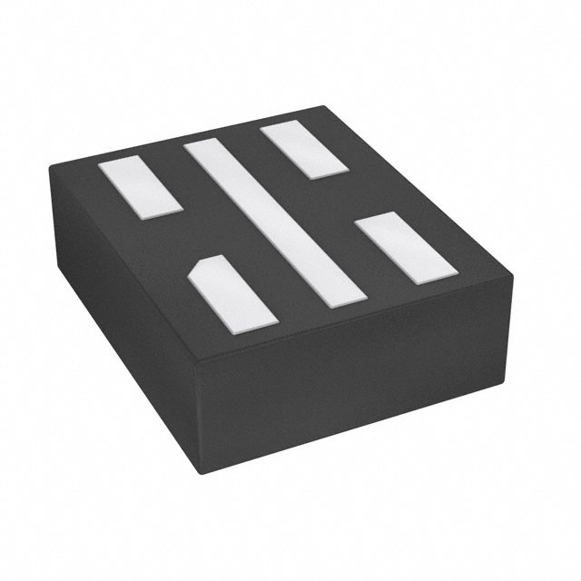
UFDFPN5
(1.7x1.4mm)
Wafer
•
•
•
•
NFC Forum Type 4 Tag, certified by the NFC Forum
ISO/IEC 14443 Type A
106 kbps data rate
Internal tuning capacitance: 50 pF
Memory
•
•
•
•
•
•
•
•
•
•
Up to 256-byte (2-Kbit) EEPROM
Support NDEF data structure
Data retention: 200 years
Endurance: 1 million erase-write cycles
Read up to 256 bytes in a single command
Write up to 54 bytes in a single command
Chaining capability
7-byte unique identifier (UID)
128-bit password protection
20-bit event counter with anti-tearing
Product identification and protection
Product status link
ST25TA512B
ST25TA02KB
ST25TA02KB-D
ST25TA02KB-P
•
TruST25™ digital signature
Package
•
UFDFPN5 ECOPACK®2
Digital output
•
GPO: configurable general purpose output
–
driven by an open drain transistor, available on ST25TA02KB-D only
–
enabling no DC consumption (CMOS output buffer), available on
ST25TA02KB-P only.
Description
The ST25TA512B and ST25TA02KB devices are NFC tag ICs, with an optional
general purpose output available on ST25TA02KB-D and ST25TA02KB-P.
They embed an up to 2 -Kbit EEPROM, and can be operated from a 13.56 MHz
RFID reader or an NFC phone.
The ST25TA512B, ST25TA02KB,
ST25TA02KB-D and ST25TA02KB-P devices are NFC Forum Type 4 Tags.
They communicate using the ISO/IEC 14443 Type A protocol, and feature a digital
signature generated by TruST25™ (a set of software and procedures) used to prove
the origin of the chip in cloning detection.
DS12365 - Rev 2 - September 2018
For further information contact your local STMicroelectronics sales office.
www.st.com
�ST25TA512B, ST25TA02KB, ST25TA02KB‑D, ST25TA02KB‑P
Functional description
1
Functional description
The ST25TA512B, ST25TA02KB, ST25TA02KB-D and ST25TA02KB-P (hereinafter referred to as ST25TAxxxB)
devices are NFC tags that can be accessed from the RF interface, based on the ISO/IEC 14443 Type A standard.
The ST25TAxxxB are compatible with the NFC Forum Type 4 Tag specifications and support all corresponding
commands.
Figure 1, Figure 2 and Figure 3 show the block diagram, respectively, of the ST25TA02KB/ST25TA512B,
ST25TA02KB-D and ST25TA02KB-P devices.
Figure 1. Block diagram - ST25TA02KB and ST25TA512B
RF interface
based on
ISO/IEC 14443
Type A standard
AC1
AC0
Analog Front-end
based on
ISO/IEC 14443
Type A standard
Power
management
unit
UID and
System
area
Digital unit
User
memory
Internal tuning
capacitance
NFC Forum
Type 4
tag protocol
Figure 2. Block diagram - ST25TA02KB-P
RF interface
based on
ISO/IEC 14443
Type A standard
AC1
AC0
Analog Front-end
based on
ISO/IEC 14443
Type A standard
Power
management
unit
UID and
System
area
Digital unit
User
memory
Internal tuning
capacitance
VDCG
GPO
f (VDCG)
GPO
VSS
DS12365 - Rev 2
NFC Forum
Type 4
tag protocol
page 2/62
�ST25TA512B, ST25TA02KB, ST25TA02KB‑D, ST25TA02KB‑P
Functional description
Figure 3. Block diagram - ST25TA02KB-D
RF interface
based on
ISO/IEC 14443
Type A standard
Analog Front-end
based on
ISO/IEC 14443
Type A standard
AC1
Power
management
unit
UID and
System
area
Digital unit
User
memory
Internal tuning
capacitance
AC0
GPO
NFC Forum
Type 4
tag protocol
VSS
Table 1. Signal names
Signal name
AC0, AC1
Function
Direction
Antenna coils
-
Supply voltage for CMOS GPO driver
Power
VSS (2)
Ground
-
GPO(2)
Interrupt output
CMOS or Open drain output
VDCG
(1)
1. Only available on ST25TA02KB-P.
2. Only available on ST25TA02KB-P and ST25TA02KB-D.
Figure 4. 5-pin package connections - ST25TA02KB-D
GPO 1
VSS 2
AC0 3
ABCD
XYZW
5 NC
5
1
2
VSS
2
2
4 AC1
4
3
Bottom view
(pads side)
Top view
(marking side)
1.
See Section 13 Package information for package dimensions, and how to identify pin 1.
Figure 5. 5-pin package connections - ST25TA02KB-P
GPO 1
VSS 2
AC0 3
ABCD
XYZW
Top view
(marking side)
1.
DS12365 - Rev 2
5 VDCG
5
1
2 VSS
2
2
4 AC1
4
3
Bottom view
(pads side)
See Section 13 Package information for package dimensions, and how to identify pin 1.
page 3/62
�ST25TA512B, ST25TA02KB, ST25TA02KB‑D, ST25TA02KB‑P
Functional mode
1.1
Functional mode
The ST25TAxxxB have only one functional mode available (see Table 2).
Table 2. Functional mode
Mode
Tag mode
Supply source
Comments
RF field only
The RF interface operates only when RF field level is sufficient.
The optional GPO open drain transistor requests an external pull-up (> 4.7 KΩ) to operate (see Figure 6).
Figure 6. Applicative example of GPO usage - ST25TA02KB-D
+
≥ 4.7 kΩ
VDD
AC0
RF
antenna
GPO
AC1
IO
VSS
ST25TA02KB-D
Microcontroller
The optional GPO CMOS driver requests an external supply to operate (see Figure 7).
DS12365 - Rev 2
page 4/62
�ST25TA512B, ST25TA02KB, ST25TA02KB‑D, ST25TA02KB‑P
Functional mode
Figure 7. Applicative example of GPO usage - ST25TA02KB-P
+
VDD
VDCG
+
AC0
RF
antenna
GPO
AC1
IO
VSS
ST25TA02KB-P
1.1.1
10 nF
Microcontroller
Tag mode
The ST25TAxxxB are supplied by the RF field and can communicate with an RF host (RFID reader or NFC
phone). The User memory can be accessed by the RF commands.
DS12365 - Rev 2
page 5/62
�ST25TA512B, ST25TA02KB, ST25TA02KB‑D, ST25TA02KB‑P
Signal description
2
Signal description
2.1
Antenna coil (AC0, AC1)
These inputs are used to connect the ST25TAxxxB devices to an external coil exclusively. It is advised not to
connect any other DC or AC path to neither AC0 nor AC1.
When correctly tuned, the coil is used to access the devices using NFC Forum Type 4 commands.
2.2
Ground (VSS), only available on ST25TA02KB-P and ST25TA02KB-D
VSS, when connected, is the reference for the VDCG supply voltage and for all pads, including AC0 and AC1.
2.3
GPO supply voltage (VDCG), only available on ST25TA02KB-P
This pin can be connected to an external DC supply voltage. It only supplies the GPO driver block.
2.3.1
Operating supply voltage VDCG
Before checking ST25TA02KB-P GPO, a valid and stable VDCG voltage within the specified [VDCG(min),
VDCG(max)] range must be applied.
To maintain a stable DC supply voltage, it is recommended to decouple the VDCG line with suitable capacitors
(usually of the order of 10 nF and 100 pF) close to the VDCG / VSS package pins.
This voltage must remain stable and valid until the end of the GPO usage by the ST25TA02KB-P.
2.3.2
Power-up conditions
The VDCG rise time must not vary faster than 1 V / μs.
2.4
General purpose output (GPO), only available on ST25TA02KB-P and
ST25TA02KB-D
The GPO pad is either an open drain pad on which an external pull-up resistor shall be connected, or a CMOS
pad with default polarity set to 0.
This pad is a configurable output signal, driven to active level when configured events occur. Its behavior is
consistent with the RF session activated and with the mode chosen by the user, see Section 7 Functional
procedures for more details.
DS12365 - Rev 2
page 6/62
�ST25TA512B, ST25TA02KB, ST25TA02KB‑D, ST25TA02KB‑P
ST25TAxxxB memory management
3
ST25TAxxxB memory management
3.1
Memory structure
The ST25TAxxxB support the NDEF Tag Application as defined in the NFC Forum Type 4 Tag. They are
composed of three files:
•
a Capability Container (CC) file
•
an NDEF file
•
a System file: this file is an ST-proprietary file
The System file contains some information on the configuration of the ST25TAxxxB devices. The CC file gives
some information about the ST25TAxxxB and the NDEF file. The NDEF file contains the User data.
3.1.1
File identifier
The file identifier is the value used in the Select command to select a file.
Table 3. File identifier
File identifier
3.1.2
Meaning
0xE101
System file
0xE103
CC file
0x0001
NDEF file
CC file layout
The CC file gives some information about the ST25TAxxxB and the NDEF file. This file is a read-only file for the
RF host and cannot be modified by issuing a write command.
The T field, Read Access and Write Access fields can be changed by the RF host by issuing a specific process
(refer to Section 7 Functional procedures).
Table 4. CC file layout
File offset
0x0000
0x0002
Meaning
Length CC file
Mapping version
Value
0x000F
(1)
0x0003
MLe: Maximum number of bytes that can be read
0x0005
MLc: Maximum number of bytes that can be written
15 bytes
0x20 or 0x10
0x00FF
Comments
(2)
V 2.0 or V 1.0
255 bytes(2)
0x0040 (3)
64 bytes(3)
0x0036
54 bytes
0x0007
0x04 (4)
T field
0x0008
0x06
L field
0x0009
0x0001
FileID
0x000B
NDEF file control TLV
0x0100(2)
0x0040(3)
FLEN: Maximum NDEF file size in Bytes
0x000D
0x00(4)
CCRD: Read access condition
0x000E
0x00(4)
CCWR: Write access condition
1. According to the reader command format the ST25TAxxxB devices will automatically align to the corresponding NFC Forum
version.
2. ST25TA02KB, ST25TA02KB-D and ST25TA02KB-P.
DS12365 - Rev 2
page 7/62
�ST25TA512B, ST25TA02KB, ST25TA02KB‑D, ST25TA02KB‑P
Memory structure
3. ST25TA512B.
4. Delivery state.
3.1.3
NDEF file layout
The NDEF file contains the NDEF message that contains the User data. The RF host can read and write data
inside the file. The first two bytes named NDEF Message Length define the size of the NDEF message. The
NDEF Message Length shall be managed by the application and the ST25TAxxxB devices do not check if its
value is relevant vs. the data written by the RF host. If the NDEF Message Length value stored in the file is
greater than FLEN-2 (NDEF Message Length > FLEN-2 can occur because of a successful UpdateBinary
command with wrong value, or because of a corrupted UpdateBinary command.) the tag handles it as an invalid
case and returns 0x00 for the byte values at offsets 0x0000 and 0x0001 in the response to a ReadBinary
command.
For more details about the read command, refer to Section 6.7.5 ReadBinary command
Table 5. NDEF file layout
File offset
Byte 0
Byte 1
Byte 2
Byte 3
0x0000
NDEF Message Length
User data
User data
0x0004
User data
User data
User data
User data
...
...
...
...
...
...
...
...
...
...
...
...
...
...
...
...
...
User data
...
0x00FC(1)
or 0x003C
(2)
1. ST25TA02KB, ST25TA02KB-D and ST25TA02KB-P.
2. ST25TA512B.
DS12365 - Rev 2
page 8/62
�ST25TA512B, ST25TA02KB, ST25TA02KB‑D, ST25TA02KB‑P
Memory structure
3.1.4
System file layout
The system file specifies the configuration of the ST25TAxxxB devices. Table 6 lists the different fields.
Table 6. Field list
File offset
Field name
No. of bytes Read access Write access
Device(s)
Delivery state
ST25TA512B
0x0000
Length system file
2
Yes
-
ST25TA02KB
ST25TA02KB-D
0x0012
ST25TA02KB-P
ST reserved
0x0002
None
1
Yes
Yes (1)
GPO Config
0x0003
0x0004
0x0007
0x0008
Yes
Yes(1)
3
Yes
None
1
Yes
None
Event Counter Config 1
20-bit counter
(MS nibble 0x0)
Product version
UID
7
Yes
None
ST25TA512B
ST25TA02KB
ST25TA02KB-D
ST25TA02KB-P
ST25TA512B
ST25TA02KB
ST25TA02KB-D
0x80
0x70 (2)
0x00
0x000000
ST25TA02KB-P 0x22 (3)
ST25TA512B
0x02E4 xx xx xx xx xx (4)
ST25TA02KB
0x02E3 xx xx xx xx xx(4)
ST25TA02KB-D 0x02F3 xx xx xx xx xx(4)
ST25TA02KB-P 0x02A3 xx xx xx xx xx(4)
ST25TA512B
0x000F
Memory Size - 1
2
Yes
None
0x003F
ST25TA02KB
ST25TA02KB-D 0x00FF
ST25TA02KB-P
0x0011
IC reference code
1
Yes
None
ST25TA512B
0xE5
ST25TA02KB
0xE2
ST25TA02KB-D 0xF2
ST25TA02KB-P 0xA2
1. Configuration bytes can be locked by setting the Most significant bit to 1. Once locked, these bytes cannot be changed
anymore.
2. Field detect as GPO configuration.
3. ST reserved.
4. x values are defined by ST to ensure UID uniqueness.
DS12365 - Rev 2
page 9/62
�ST25TA512B, ST25TA02KB, ST25TA02KB‑D, ST25TA02KB‑P
Read and write access rights to the NDEF file
Table 7. Details about the Counter configuration field
File offset
b7
b6-b2
b1
b0
0x0003
Counter configuration lock bit:
•
0b0: unlocked
•
0b1: locked
0b00000 (ST reserved)
Counter enable:
•
0b0: disable
•
0b1: enable
Counter increment:
•
0b0: on Read
•
0b1: on Write
Table 8. Details about the GPO field
File offset
b7
b6-b4
b3-b0
0x0002
GPO configuration lock bit:
•
0b0: unlocked
•
0b1: locked
GPO configuration:
•
0b000: Not used
•
0b001: Session opened
•
0b010: WIP
•
0b011: MIP
•
0b100: Interrupt
•
0b101: State Control
•
0b110: RF Busy
•
0b111: Field Detect
0b0000
(ST reserved)
3.2
Read and write access rights to the NDEF file
The NDEF file can be protected for read or write accesses with passwords that the host shall present before
accessing the NDEF file. There are two 128-bit passwords, one for the read access and the other one for the
write access.
An NDEF file can also be locked for read or write accesses. Thus, the host cannot access the NDEF file.
The read password shall be sent to the ST25TAxxxB devices before reading a
read-protected NDEF file.
The write password shall be sent to the ST25TAxxxB devices before writing a
write-protected NDEF file. The write password shall be sent to change the read or write protection mode. The
access rights are only relevant for the NDEF file. If the Verify command is used with the CC, System or no file
selected, an error is responded by the tag.
DS12365 - Rev 2
page 10/62
�ST25TA512B, ST25TA02KB, ST25TA02KB‑D, ST25TA02KB‑P
Read and write access rights to the NDEF file
3.2.1
Read and Write protection modes
Three protection modes are defined for each of the Read and Write access rights to the NDEF file:
•
UNPROTECTED
•
PROTECTED
•
FORBIDDEN
The Read/Write protection mode is identified by the R-APDU value responded to a Verify command (see
Section 6.8.1 Verify command).
Table 9. Read protection modes
Mode
Verify (P1P2=0x0001) R-APDU
Meaning
READ UNPROTECTED
0x9000
Read access without any security (delivery state)
READ PROTECTED
0x6300
Read access protected by password
READ FORBIDDEN
0x6984
Read access forbidden (permanent state)
Table 10. Write protection modes
Mode
3.2.2
Verify (P1P2=0x0002) R-APDU
Meaning
WRITE UNPROTECTED
0x9000
Write access without any security (delivery state)
WRITE PROTECTED
0x6300
Write access protected by password
WRITE FORBIDDEN
0x6984
Write access forbidden (permanent state)
Read and Write access conditions
The CCRD and CCWR bytes (see Table 3. File identifier) in the CC file are used to identify the Read and Write
access conditions for the NDEF message as defined in the NFC Forum Type 4 Tag specification. The
ST25TAxxxB support one read condition value and two write condition values.
Table 11 and Table 12 show how these condition values are mapped to the read and write protection modes
defined in Section 3.2.1 Read and Write protection modes.
Caution:
As several protection modes may be mapped to a single condition value, the Read and Write access condition
values are not to be used to identify the protection modes.
Table 11. Read access conditions (CCRD values)
Value
Read protection modes
UNPROTECTED, PROTECTED, FORBIDDEN (1)
0x00
1. Refer to Section 3.2.1 Read and Write protection modes to discriminate between the protection modes.
Table 12. Write access conditions (CCWR values)
Value
Write protection modes
0x00
UNPROTECTED
0xFF
PROTECTED, FORBIDDEN(1)
1. Refer to Section 3.2.1 Read and Write protection modes to discriminate between the protection modes.
DS12365 - Rev 2
page 11/62
�ST25TA512B, ST25TA02KB, ST25TA02KB‑D, ST25TA02KB‑P
Read and write access rights to the NDEF file
3.2.3
Changing the read protection mode
The state diagram of Figure 8 shows how to change the read protection mode of the NDEF file.
Figure 8. Changing the read protection mode
READ UNPROTECTED(5)
CCRD: 0x00
SW1SW2: 0x9000
Protect the
NDEF file(1)
Lock the
NDEF file(3)
Unprotect the
NDEF file(2)
READ PROTECTED(4)
CCRD: 0x00
SW1SW2: 0x6300
Lock the NDEF file(3)
READ FORBIDDEN(4)
CCRD: 0x00
SW1SW2: 0x6984
CCRD: byte at offset 0x000D in the CC file
SW1SW2: response to the Verify (Read protection) command
1.
2.
3.
4.
5.
3.2.4
See the procedure to protect the read access (Section 7.1 Protecting an NDEF file).
See the procedure to unprotect the read access (Section 7.3 Unprotecting an NDEF file).
See the procedure to forbid the read access (Section 7.4 Locking an NDEF file).
Proprietary state, not defined by NFC Forum Type 4 Tag.
Delivery state.
Changing the write protection mode
The state diagram of Figure 9 shows how to change the write protection mode of the NDEF file.
Figure 9. Changing the write protection mode
WRITE UNPROTECTED(5)
CCWR: 0x00
SW1SW2: 0x9000
Protect the
NDEF file(1)
Lock the
NDEF file(3)
Unprotect the
NDEF file(2)
WRITE PROTECTED(4)
CCWR: 0xFF
SW1SW2: 0x6300
Lock the NDEF file
(3)
WRITE FORBIDDEN
CCWR: 0xFF
SW1SW2: 0x6984
CCWR: byte at offset 0x000E in the CC file
SW1SW2: response to the Verify (Write protection) command
1.
2.
DS12365 - Rev 2
See the procedure to protect the write access (Section 7.1 Protecting an NDEF file).
See the procedure to unprotect the write access (Section 7.3 Unprotecting an NDEF file).
page 12/62
�ST25TA512B, ST25TA02KB, ST25TA02KB‑D, ST25TA02KB‑P
Granted access life time
3.
4.
5.
3.3
See the procedure to forbid the write access (Section 7.4 Locking an NDEF file).
Proprietary state, not defined by NFC Forum Type 4 Tag.
Delivery state.
Granted access life time
When the NDEF file is in a READ or WRITE PROTECTED state, the corresponding file access is granted starting
from the first successful password presentation (see Section 7.1 Protecting an NDEF file), and until one of the
following events occurs:
•
an RF field shutdown
•
a successful DESELECT command
•
a successful NDEF Tag Application Select command (no file selected)
•
successful Capability Container Select or System File Select command (other file selected)
•
a wrong password presentation (security session closed)
When the NDEF file is in a READ or WRITE FORBIDDEN state, the corresponding file access is never granted.
3.4
NDEF file passwords
Two passwords are available on the ST25TAxxxB devices:
•
Read password: protects the read access to the NDEF file
•
Write password: protect the write access to the NDEF file and the setting of the read and write protection
modes (see Section 7.1 Protecting an NDEF file and Section 7.2 Accessing a protected NDEF file)
The length of a password is 128 bits (16 bytes).
A password is presented using the Verify command (see Section 6.8.1 Verify command).
After three consecutive authentication failures for a given password, further attempts will fail until the following
sequence of events occurs:
•
tag set in Standby power mode (RF field shutdown or DESELECT command)
•
tag activation (anticollision and RATS commands)
•
successful NDEF Tag Application Select command
•
successful NDEF Select command
Note:
DS12365 - Rev 2
The delivery state for all passwords is 0x00000000000000000000000000000000.
page 13/62
�ST25TA512B, ST25TA02KB, ST25TA02KB‑D, ST25TA02KB‑P
Specific features
4
Specific features
4.1
Read/Write counter
A 20-bit counter can track the read or write events on the NDEF file.
It benefits from an anti-tearing mechanism, that ensures the consistency of the counter, even if there has been an
electrical problem during its increment.
The value of the Read/Write counter can be checked by any application, by reading suitable bytes in System file
(see Section 3.1.4 System file layout).
If enabled, the Read/Write counter will be incremented on the first event (exclusively read / write) performed on
the NDEF File, after a successful NDEF Tag Application Select command. Following read/write events will not
modify the counter value until a new successful NDEF Tag Application Select command is issued.
The counter is reset when it is disabled.
Apart from these procedures, there is no way to act on the value of this counter.
The Read/Write counter can be configured through a specific byte in System file (see Section 3.1.4 System file
layout).
This configuration byte allows to:
•
Enable or disable this counter
•
Define if the counter must be incremented on a read or write sequence
•
Definitively lock this configuration byte
Caution:
Once this configuration byte is locked, it cannot be changed anymore: the counter will behave accordingly.
If enabled, the Read/Write counter will have an impact on the execution time of the event being countered: the
counter increment needs some write cycles of specific EEPROM cells automatically managed by ST25TAxxxB,
this increases the total time before the response is sent to the reader.
As a consequence, an S(WTX) request can be issued on the command that will increment the counter (see
Section 6.4 S-Block format).
4.2
General purpose output (GPO), only available on ST25TA02KB-D/P
The GPO pad is either a CMOS pad (ST25TA02KB-P) or an open drain pad (ST25TA02KB-D).
In case of CMOS GPO active state is 1 and inactive state is 0.
In case of open drain an external pull-up shall be connected to it. In this case, active state is 0 and inactive state
is 1. If no pull-up is used the active state is 0, but inactive state is HZ.
This pad is a configurable output signal, driven to the alternate polarity when configured event occur. Its behavior
is consistent with the RF session activated and with the mode chosen by the user.
The user can select one of these configurations (Table 68. GPO timings measurement ):
•
Inactive: the state of the GPO pad is always inactive
•
SessionOpen: an RF session is ongoing.
•
MIP (NDEF Message updating In Progress): the RF host is writing an NDEF length different from 0x0000.
This mode can be used to detect when the RF host changes the NDEF message as defined by the NFC
Forum.
•
WIP (Writing In Progress): the ST25TA02KB-D/P is executing a writing operation.
•
INT (interrupt): the RF host can force the ST25TA02KB-D/P to send an alternate pulse on the GPO pin.
•
State mode: the RF host can control the state of the GPO pad during the RF session.
•
RF busy: an RF host is communicating with the ST25TA02KB-D/P.
•
Field detection: the RF field is sufficient to establish an RF communication with the ST25TA02KB-D/P.
GPO configuration byte can be locked, by setting its Most Significant Bit to 1 (1xxx 0000 b). Once locked, this
byte cannot be changed anymore.
DS12365 - Rev 2
page 14/62
�ST25TA512B, ST25TA02KB, ST25TA02KB‑D, ST25TA02KB‑P
General purpose output (GPO), only available on ST25TA02KB-D/P
4.2.1
Inactive configuration (GPO field = 0x00 or 0x80)
When the GPO is configured as "Inactive", it remains in inactive state regardless of the events on the RF interface
(except setting the GPO to another configuration).
4.2.2
Session Open configuration (GPO field = 0x10 or 0x90)
When the GPO is configured as “Session Open”, it goes to the active state when an RF session is ongoing (see
Figure 10 or Figure 11).
An RF session is taken when the ST25TA02KB-D/P receives a valid Select Application. The session is released
when:
•
ST25TA02KB-D/P receives a valid Deselect command
•
RF field becomes OFF
GPO is driven to active state after a delay (1.) when the session is open.
GPO is released after a delay (2.) when the session is released.
RF Session
GPO as
Session Open
1.
2.
(1)
Deselect
Anticollision and
Application select
Deselect
RF channel
Anticollision and
Application select
Figure 10. CMOS GPO configured as Session Open (GPO field = 0x10 or 0x90)
RF Session
(2)
CmdEOFtoGPhigh (RF command End of frame to GPORF Session pad high).
CmdEOFtoGPlow (RF command End of frame to GPORF Session pad low).
RF Session
GPO as
Session Open
1.
2.
DS12365 - Rev 2
(1)
Deselect
Anticollision
Application select
NDEF select
Deselect
RF channel
Anticollision
Application select
NDEF select
Figure 11. Open drain GPO configured as Session Open (GPO field = 0x10 or 0x90)
RF Session
(2)
CmdEOFtoGPlow (RF command End of frame to GPORF Session pad low).
CmdEOFtoGPHZ (RF command End of frame to GPORF Session pad HZ).
page 15/62
�ST25TA512B, ST25TA02KB, ST25TA02KB‑D, ST25TA02KB‑P
General purpose output (GPO), only available on ST25TA02KB-D/P
4.2.3
WIP Writing in Progress configuration (GPO field = 0x20 or 0xA0)
When the GPO is configured as “WIP”, it goes to the active state state during an RF writing operation (see
Figure 12 or Figure 13).
During an RF session, when the ST25TA02KB-D/P updates a file, the GPO is driven in active state after a delay
(1.) following the beginning of the correspondent UpdateBinary command execution.
GPO will remain in active state during the writing time (2.), before being released.
Figure 12. CMOS GPO configured as WIP (GPO field = 0x20 or 0xA0)
RF channel
(1)
Update
command
End of writing
operation
Any other
command
GPO as WIP
(2)
1.
2.
CmdEOFtoGPhigh (RF Command End of frame to GPO high).
Writing time duration.
Figure 13. Open drain GPO configured as WIP (GPO field = 0x20 or 0xA0)
RF channel
(1)
Update
command
End of writing
operation
Any other
command
GPO as WIP
(2)
1.
2.
DS12365 - Rev 2
CmdEOFtoGPlow (RF Command End of frame to GPO low).
Writing time duration.
page 16/62
�ST25TA512B, ST25TA02KB, ST25TA02KB‑D, ST25TA02KB‑P
General purpose output (GPO), only available on ST25TA02KB-D/P
4.2.4
MIP NDEF Message writing in Progress configuration (GPO field = 0x30 or 0xB0)
When the GPO is configured as MIP, its state goes to the active state when the RF host writes the NDEF length to
another value than 0x0000 (see Figure 14 or Figure 15).
During an RF session, when the ST25TA02KB-D/P changes an NDEF file and updates the NDEF length with a
value different from 0x0000, the GPO is driven in active state after a delay (1.) following the beginning of the
correspondent UpdateBinary command execution.
GPO will remain in active state during the writing time (2.), before being released.
Figure 14. CMOS GPO configured as MIP (GPO field = 0x30 or 0xB0)
RF channel
Update the NDEF
length ≠ 0x0000
ST25TA02KB-P
response
Any other
command
GPO as MIP
(1)
(2)
1.
2.
CmdEOFtoGPhigh (RF command End of frame to GPO high).
Writing time duration.
Figure 15. Open drain GPO configured as MIP (GPO field = 0x30 or 0xB0)
RF channel
Update the NDEF
length != 0x0000
ST25TA02KB-D
response
Any other
command
GPO as MIP
(1)
(2)
1.
2.
DS12365 - Rev 2
CmdEOFtoGPlow (RF command End of frame to GPO low).
Writing time duration.
page 17/62
�ST25TA512B, ST25TA02KB, ST25TA02KB‑D, ST25TA02KB‑P
General purpose output (GPO), only available on ST25TA02KB-D/P
4.2.5
INT Interrupt configuration (GPO field = 0x40 or 0xC0)
The RF host can send a pulse on the GPO pad. The GPO pad goes to active state at the end of the command
and goes to the inactive state at the end of the ST25TA02KB-D/P response (see Figure 16 or Figure 17).
During an RF session, when the ST25TA02KB-D/P receives a valid SendInterrupt command, the GPO pin is
driven in active state (1.). Then the GPO pin is released at the end of the response (2.).
Figure 16. CMOS GPO configured as INT (GPO field = 0x40 or 0xC0)
RF channel
ST25TA02KB-P
response
Send
Interrupt
(1)
Any other
operation
(2)
GPO as INT
1.
2.
CmdEOFtoGPhigh (RF command End of frame to GPO high).
RespEOFtoGPlow.
Figure 17. Open drain GPO configured as INT (GPO field = 0x40 or 0xC0)
RF channel
Send
Interrupt
ST25TA02KB-D
response
Any other
operation
GPO as INT
(1)
DS12365 - Rev 2
(2)
page 18/62
�ST25TA512B, ST25TA02KB, ST25TA02KB‑D, ST25TA02KB‑P
General purpose output (GPO), only available on ST25TA02KB-D/P
4.2.6
State Control configuration (GPO field = 0x50 or 0xD0)
When the GPO is configured as State Control, the RF host can control the state of the GPO by sending a
dedicated command (see Figure 18 or Figure 19).
During an RF session, the ST25TA02KB-D/P can control the GPO pin. After receiving a valid StateControl
command with Data=0x00, the GPO pin is driven in active state after a delay (1.). The GPO will be released after
a valid StateControl command with Data=0x01 or after a Power off.
Figure 18. CMOS GPO configured as State Control (GPO field = 0x50 or 0xD0)
RF channel
StateControl (0x00)
command
GPO as
State Control
1.
2.
Any other
command
StateControl (0x01)
command
(1)
(2)
CmdEOFtoGPhigh (RF Reset GPO command End of frame to GPO high).
CmdEOFtoGPlow (RF Set GPO command End of frame to GPO low).
Figure 19. Open drain GPO configured as State Control (GPO field = 0x50 or 0xD0)
RF channel
StateControl
(0x00) command
GPO as
State Control
1.
2.
DS12365 - Rev 2
Any other
command
StateControl
(0x01) command
(1)
(2)
CmdEOFtoGPlow (RF Reset GPO command End of frame to GPO low).
CmdEOFtoGPHZ (RF Set GPO command End of frame to GPO HZ).
page 19/62
�ST25TA512B, ST25TA02KB, ST25TA02KB‑D, ST25TA02KB‑P
General purpose output (GPO), only available on ST25TA02KB-D/P
4.2.7
RF busy configuration (GPO field = 0x60 or 0xE0)
When the GPO is configured as RF busy, the GPO goes to the active state, both when the ST25TA02KB-D/P is
processing an RF command or when an RF session is ongoing (see Figure 20 or Figure 21).
When an RF field is present, the GPO is driven in active state after a delay (1.) when the ST25TA02KB-D/P
detects the first command. If the RF session is ongoing and the ST25TA02KB-D/P receives a not-supported
command, GPO remains active. It will be released only at the end of the RF session, after (2.).
Figure 20. CMOS GPO configured as RF busy (GPO field = 0x60 or 0xE0)
(1)
RF channel
(2)
(1)
(2)
SensReq
and
SensRes
RF command
not supported
RF command
SLP_REQ
or S(DES)
or bad command
or RF Field OFF
GPO as RF busy
1.
2.
CmdSOFtoGPhigh (RF command Start of frame to GPO high).
CmdEOFtoGPlow (RF command End of frame to GPO low).
Figure 21. Open drain GPO configured as RF busy (GPO field = 0x60 or 0xE0)
RF channel
(1)
(2)
RF command
not supported
(1)
SensReq
and
SensRes
RF
command
(2)
SLP_REQ
or S(DES)
or bad command
or RF Field OFF
GPO as RF busy
1.
2.
DS12365 - Rev 2
CmdSOFtoGPlow (RF command Start of frame to GPO low).
CmdEOFtoGPHZ (RF command End of frame to GPO HZ).
page 20/62
�ST25TA512B, ST25TA02KB, ST25TA02KB‑D, ST25TA02KB‑P
TruST25™ digital signature feature
4.2.8
Field detect configuration (GPO field = 0x70 or 0xF0)
When the GPO is configured as Field detect, the GPO goes to the active state when ST25TA02KB-D/P detects
an RF Field (see Figure 22 or Figure 23).
When an RF field is present, GPO is driven in active state after a delay when the ST25TA02KB-D/P detects this
field. Whatever the activity during the RF field detection (communication with the reader or not), GPO will stay
active. It will be released when the ST25TA02KB-D/P leaves the RF field.
Figure 22. CMOS GPO configured as Field detect (GPO field = 0x70 or 0xF0)
RF field
Hmin
VDCG
GPO
VSS
tFDETON
tFDETOFF
Figure 23. Open drain GPO configured as Field detect (GPO field = 0x70 or 0xF0)
RF field
Hmin
HZ
GPO
VSS
tFDETON
4.3
tFDETOFF
TruST25™ digital signature feature
The ST25TAxxxB devices support the TruST25™ digital signature feature, which allows the user to verify the
authenticity of the device, based on a unique digital signature.
TruST25™ solution encompasses secure industrialization processes and tools deployed by STMicroelectronics to
generate, store and check the signature in the device.
Implementation details are described in application note AN5101, contact your STMicroelectronics sales office to
get this document.
DS12365 - Rev 2
page 21/62
�ST25TA512B, ST25TA02KB, ST25TA02KB‑D, ST25TA02KB‑P
Communication mechanism
5
Communication mechanism
This section describes the principle of communication between an RF host and the ST25TAxxxB devices.
5.1
Master and slave
The ST25TAxxxB act as slave devices on the RF channel and therefore wait for a command from the RF host
before sending a response.
The RF host shall generate the RF field and the RF commands.
DS12365 - Rev 2
page 22/62
�ST25TA512B, ST25TA02KB, ST25TA02KB‑D, ST25TA02KB‑P
RF command sets
6
RF command sets
This section describes the ST25TAxxxB command sets that can be issued by the RF host.
There are three command families:
•
the NFC Forum Type 4 Tag command set
•
the ISO/IEC 7816-4 command set
•
the ST-proprietary command set
The NFC Forum Type 4 Tag command set and the ISO/IEC 7816-4 command set use the
I-Block format. For more details about the I-Block format, refer to Section 6.2 I-Block format.
Two other command formats exist:
•
the commands using the R-Block format
•
the commands using the S-Block format
For more details about these formats, refer to Section 6.3 R-Block format and to Section 6.4 S-Block format.
This section gives a brief description of the RF host commands. The format of these command sets is the I-Block
format.
Table 13 lists the RF command sets.
Table 13. RF command sets
Family command set
Command name
Class Instruction
byte
Brief description
code
NDEF Tag Application Select
0x00
0xA4
NDEF Tag Application Select
CC select
0x00
0xA4
Selects the CC file
NFC Forum
NDEF Select
0x00
0xA4
Selects the NDEF file
Type 4 Tag
System select
0x00
0xA4
Selects the system file
ReadBinary
0x00
0xB0
Reads data from file
UpdateBinary
0x00
0xD6
Writes or erases data to an NDEF file
Verify
0x00
0x20
Checks the right access of an NDEF file or sends a password
ChangeReferenceData
0x00
0x24
Changes a Read or Write password
EnableVerificationRequirement
0x00
0x28
Activates the password security
DisableVerificationRequirement 0x00
0x26
Disables the password security
EnablePermanentState
0xA2
0x28
Enables the READ FORBIDDEN or the WRITE FORBIDDEN
protection mode
ExtendedReadBinary
0xA2
0xB0
Reads data from file
UpdateFileType
0xA2
0xD6
Sets file type to NDEF or to proprietary
StateControl
0xA2
0xD6
Drives the state of the GPO pin(1)
SendInterrupt
0xA2
0xD6
Generates a pulse on the GPO pin(1)
ISO/IEC 7816-4
ST-proprietary
1. Available on ST25TA02KB-D/P only
DS12365 - Rev 2
page 23/62
�ST25TA512B, ST25TA02KB, ST25TA02KB‑D, ST25TA02KB‑P
Structure of the command sets
6.1
Structure of the command sets
The exchange of data between the RF host and the ST25TAxxxB uses three kinds of data formats, called blocks:
•
I-Block (Information block): to exchange the command and the response
•
R-Block (Receive ready block): to exchange positive or negative acknowledgment
•
S-Block (Supervisory block): to use either the Deselect command or the Frame Waiting eXtension (WTX)
command or response
This section describes the structure of I-Block, R-block and S-Block. This format is used for the application
command set.
6.2
I-Block format
The I-Block is used to exchange data between the RF host and the ST25TAxxxB. It is composed of three fields,
as detailed in Table 14.
Table 14. I-Block format
SoD
Name
Length
Payload
EoD
PCB
DID
-
CRC
1 byte
1 byte
1 to 251 bytes
2 bytes
PCB field
DID field (optional)
RF host to ST25TAxxxB: C-APDU
ST25TAxxxB to RF host: R-APDU
2 CRC bytes
Table 15. PCB field of the I-Block format
b7-b6
b5
b4
b3
b2
b1
b0
0b00
0
0
X
0
1
X
I-Block
RFU
Must be set to 0
DID field is present, if bit is set
Must be set to 0
Must be set to 1
Block number (1)
1. Follow ISO 14443_4 Block numbering rules (see note)
Note:
Block numbering rules:
Reader rules:
•
•
DS12365 - Rev 2
Rule A:The Reader block number shall be initialized to 0.
Rule B:When an I-block or an R(ACK) block with a block number equal to the current block number is
received, the Reader shall toggle the current block number before optionally sending a block to the
ST25TAxxxB.
page 24/62
�ST25TA512B, ST25TA02KB, ST25TA02KB‑D, ST25TA02KB‑P
I-Block format
ST25TAxxxB rules:
•
•
Rule C: The ST25TAxxxB block number shall be initialized to 1 at activation.
Rule D: When an I-block is received, the ST25TAxxxB shall toggle its block number before sending a block.
Note:
The ST25TAxxxB may check if the received block number is not in compliance with Reader rules to decide
neither to toggle its internal block number nor to send a response block.
•
Rule E: When an R(ACK) block with a block number not equal to the current ST25TAxxxB block number is
received, the ST25TAxxxB shall toggle its block number before sending a block.
Note:
There is no block number toggling when an R(NAK) block is received.
When the RF host sends a command to the ST25TAxxxB, the format of the payload is the C-APDU.
When the ST25TAxxxB sends a command to the RF host, the format of the payload is the R-APDU.
6.2.1
C-APDU: payload format of a command
The C-APDU format is used by the RF host to send a command to the ST25TAxxxB. Table 16 describes its
format.
Table 16. C-APDU format
Name
Length
Payload field
CLA
INS
P1
P2
LC
Data
Le
1 byte
1 byte
1 byte
1 byte
1 byte
Lc byte
1 byte
Class byte
- 0x00: standard command
- 0xA2: ST command
Instruction byte
Param Byte 1
Param Byte 2
Number of bytes of the Data field
Data bytes
Number of bytes to be read in the ST25TAxxxB memory
1. See Table 13. RF command sets.
DS12365 - Rev 2
page 25/62
�ST25TA512B, ST25TA02KB, ST25TA02KB‑D, ST25TA02KB‑P
R-Block format
6.2.2
R-APDU: payload format of a response
The ST25TAxxxB use the I-Block format to reply to a command that has used the I-Block format. This format is
described in Table 17.
Table 17. R-APDU format
Payload field
Name
Length
Data (optional)
SW1
SW2
Le byte
1 byte
1 byte
Data
Status byte 1
Status byte 2
6.3
R-Block format
The R-Block is used to convey positive or negative acknowledgment between the RF host and the ST25TAxxxB.
Table 18. R-Block format
NFC frame
Length
SoD
-
EoD
PCB
DID
Payload
CRC
1 byte
1 byte
0 byte
2 bytes
R(ACK) without the DID field: 0xA2 or 0xA3
R(ACK) with the DID field: 0xAA or 0xAB
R(NAK) without the DID field: 0xB2 or 0xB3
R(NAK) with the DID field: 0xBA or 0xBB
DID field (optional)
2 CRC bytes
There are two kinds of R-Blocks:
•
R(ACK): the acknowledgment block sent by the RF host or by the ST25TAxxxB
•
R(NAK): the non-acknowledgment block sent by the RF host
DS12365 - Rev 2
page 26/62
�ST25TA512B, ST25TA02KB, ST25TA02KB‑D, ST25TA02KB‑P
S-Block format
Table 19. PCB field of the R-Block format
b7-b6
b5
b4
b3
b2
b1
b0
0b10
1
X
X
0
1
X
R-Block
Must be set to 1.
0: ACK
1: NAK
0: DID field is not present
1: DID field is present
Must be set to 0
Must be set to 1
Block number
6.4
S-Block format
The S-Block is used to exchange control information between a reader and a contactless tag.
Table 20. S-Block format
NFC frame
Length
SoD
-
EoD
PCB
DID
Payload
CRC
1 byte
1 byte
1 byte
2 bytes
S(DES) without the DID field : 0xC2
S(DES) with the DID field : 0xCA
S(WTX) without the DID field : 0xF2
S(WTX) with the DID field : 0xFA
DID field (optional)
WTX field (optional) (1)
2 CRC bytes
1. This field is present when b5-b4 bits are set to 0b11 (S-Block is a WTX). See Table 21. PCB field of the S-Block format.
There are two requests using the S-Block format:
•
S(DES): the Deselect command
•
S(WTX): the Waiting Frame eXtension command or response.
A Waiting Time eXtension request occurs in RF when the operating time needed by the ST25TAxxxB is greater
than 19.2 ms.
The WTX field indicates the increase time factor to be used in this command execution (FDTtemp = WTX *
19.2 ms). WTX depends on FWI.
DS12365 - Rev 2
page 27/62
�ST25TA512B, ST25TA02KB, ST25TA02KB‑D, ST25TA02KB‑P
S-Block format
Table 21. PCB field of the S-Block format
b7-b6
b5-b4
b3
b2
b1
b0
0b11
X
X
0
1
0
S-Block
0b00: Deselect
0b11: WTX
0: DID field is not present
1: DID field is present
Must be set to 0
Must be set to 1
Must be set to 0
Note:
DS12365 - Rev 2
After receiving the deselect command, the ST25TAxxxB enter the Standby power mode.
In response to a RATS command, the ST25TAxxxB return the FWI parameter (default frame waiting time used);
when the ST25TAxxxB need more time for a command execution, they request a frame waiting time extension
by responding 0xF2 0xWTX
(Request waiting time = FWI * WTX). If the reader accepts the ST25TAxxxB request, it acknowledges the
request by sending the command 0xF2 0xWTX. The frame waiting time becomes FWI * WTX for the current
command only.
page 28/62
�ST25TA512B, ST25TA02KB, ST25TA02KB‑D, ST25TA02KB‑P
CRC of the RF frame
6.5
CRC of the RF frame
The two CRC bytes check the data transmission between the RF host and the ST25TAxxxB. For the RF frame,
the CRC is computed on all the data bits in the frame, excluding parity bits, SOF and EOF, and the CRC itself.
The CRC is as defined in ISO/IEC 13239. The initial register content shall be 0x6363 and the register content
shall not be inverted after calculation.
6.6
Status and error codes
This section lists the status and the error codes of the ST25TAxxxB.
Table 22. Status code of the ST25TAxxxB
SW1
Value
0x90
SW2
0x00
Comment
Command completed successfully
Table 23. Error codes of the ST25TAxxxB
Length
DS12365 - Rev 2
SW1
SW2
1 byte
1 byte
Comment
Value
0x63
0x00
Password is required
Value
0x63
0xCX
Value
0x65
0x81
Unsuccessful updating
Value
0x67
0x00
Wrong frame length
Value
0x69
0x81
Command is incompatible with the file structure
Value
0x69
0x82
Security status not satisfied
Value
0x69
0x84
Reference data not usable
Value
0x69
0x85
Conditions of use not satisfied
Value
0x6A
0x80
Incorrect parameters Le or Lc
Value
0x6A
0x82
File or application not found
Value
0x6A
0x84
File overflow (Lc error)
Value
0x6A
0x86
Incorrect P1 or P2 values
Value
0x6D
0x00
INS field not supported
Value
0x6E
0x00
Class not supported
Password is incorrect, X further retries allowed
(X can take values 0, 1 or 2)
page 29/62
�ST25TA512B, ST25TA02KB, ST25TA02KB‑D, ST25TA02KB‑P
NFC Forum Type 4 Tag protocol
6.7
NFC Forum Type 4 Tag protocol
The ST25TAxxxB command set is built to easily support the NFC Forum Type 4 Tag protocol.
6.7.1
NDEF Tag Application Select command
The RF host shall send this command to activate the NDEF Tag Application.
To activate the NDEF Tag Application, the RF host sends the Select command in addition to the sequence defined
in the NFC Forum digital protocol.
Table 24 and Table 25 respectively define the C-APDU and R-APDU of the NDEF Tag Application Select
command.
Table 24. C-APDU of the NDEF Tag Application Select command
Name
-
CLA
INS
0x00
P1
0xA4
P2
0x04
0x00
Lc
0x07
Data
0xD2760000850101
Le
0x00
Class byte
Select instruction code
P1 field
P2 field
Number of bytes of data
Application ID
Le field
Table 25. R-APDU of the NDEF Tag Application Select command
Data
DS12365 - Rev 2
SW1
SW2
Comment
Length
-
1 byte
1 byte
-
Value
-
0x90
0x00
Command completed
Value
-
0x6A
0x82
NDEF Tag Application not found
Value
-
0x6D
0x00
Class not supported
Value
-
0x6*
0x**
Refer to Section 6.6 Status and error codes
page 30/62
�ST25TA512B, ST25TA02KB, ST25TA02KB‑D, ST25TA02KB‑P
NFC Forum Type 4 Tag protocol
6.7.2
Capability Container Select command
The RF host uses the Capability Container Select procedure to select the capability container (CC) file.
The CC file is selected when this command returns "command completed" in the R-APDU. Table 26 and Table 27
respectively define the C-APDU and R-APDU of the Capability Container Select command.
Table 26. C-APDU of the Capability Container Select command
Name
CLA
-
0x00
INS
P1
0xA4
0x00
P2
0x0C
Lc
0x02
Data
0xE103
Le
-
Class byte
Select instruction code
P1 field
P2 field
Number of bytes of data
CC file ID
(empty field)
Table 27. R-APDU of the Capability Container Select command
Data
6.7.3
SW1
SW2
Comment
Length
-
1 byte
1 byte
-
Value
-
0x90
0x00
Command completed
Value
-
0x6A
0x82
File or application not found
Value
-
0x6D
0x00
Class not supported
Value
-
0x6*
0x**
Refer to Section 6.6 Status and error codes
NDEF Select command
The RF host uses the NDEF Select command to select the NDEF file.
The NDEF file is selected when this command returns “command completed” in the R-APDU. Table 28 and
Table 29 respectively define the C-APDU and R-APDU of the NDEF Select command.
Table 28. C-APDU of the NDEF Select command
Name
-
CLA
0x00
INS
0xA4
P1
0x00
P2
0x0C
Lc
0x02
Data
0x0001
Le
-
Class byte
Select instruction code
P1 field
P2 field
Number of bytes of data
0x0001: NDEF file
(empty field)
DS12365 - Rev 2
page 31/62
�ST25TA512B, ST25TA02KB, ST25TA02KB‑D, ST25TA02KB‑P
NFC Forum Type 4 Tag protocol
Table 29. R-APDU of the NDEF Select command
Data
6.7.4
SW1
SW2
Comment
Length
-
1 byte
1 byte
-
Value
-
0x90
0x00
Command completed
Value
-
0x6A
0x82
File or application not found
Value
-
0x6*
0x**
Refer to Section 6.6 Status and error codes
System File Select command
The RF host uses this command to select the system file.
The System file is selected when this command returns "command completed" in the
R-APDU.
Table 30 and Table 31 respectively define the C-APDU and R-APDU of the System File Select command.
Table 30. C-APDU of the System File Select command
Name
CLA
-
INS
0x00
P1
0xA4
0x00
P2
0x0C
Lc
0x02
Data
0xE101
Le
-
Class byte
Select instruction code
P1 field
P2 field
Number of bytes of data
System file ID
(empty field)
Table 31. R-APDU of the System File Select command
Data
6.7.5
SW1
SW2
Comment
Length
-
1 byte
1 byte
-
Value
-
0x90
0x00
Command completed
Value
-
0x6A
0x82
System file not found, no data is returned
Value
-
0x6*
0x**
Refer to Section 6.6 Status and error codes
ReadBinary command
On receiving the ReadBinary command, the ST25TAxxxB read the requested memory field and send back its
value in the R-APDU response.
Before sending a ReadBinary command, a file shall be selected by using a Select command.
The Response of the ReadBinary command is successful when the start offset P1P2 is lower than LEN: the
length of the selected file(For more details about CC file, refer to Section 3.1.2 CC file layout. For more details
about NDEF file, refer to Section 3.1.3 NDEF file layout. For more details about System file, refer to
Section 3.1.4 System file layout.)
Table 32 and Table 33 respectively define the C-APDU and R-APDU of the ReadBinary command.
DS12365 - Rev 2
page 32/62
�ST25TA512B, ST25TA02KB, ST25TA02KB‑D, ST25TA02KB‑P
NFC Forum Type 4 Tag protocol
Table 32. C-APDU of the ReadBinary command
Name
CLA
INS
P1 and P2
Lc
Data
Le
-
0x00
0xB0
2 bytes
-
-
1 byte
Class byte
Read instruction code
Offset in the file selected 0x0000 ≤ P1P2 < LEN
(empty field)
(empty field)
Number of bytes to read: 0x00 ≤ Le ≤ MLe
Table 33. R-APDU of the ReadBinary command
Data
6.7.6
SW1
SW2
Comment
Length
-
1 byte
1 byte
-
Value
Content read
0x90
0x00
Command completed
Value
-
0x69
0x85
Read access forbidden
Value
-
0x6A
0x80
Wrong Le value (> MLe)
Value
-
0x69
0x82
Security status not satisfied
Value
-
0x6A
0x82
File or application not found
Value
-
0x6A
0x86
Wrong start address (P1P2 ≥ LEN)
Value
-
0x6*
0x**
Refer to Section 6.6 Status and error codes
UpdateBinary command
On receiving the UpdateBinary command, the ST25TAxxxB write the data field into the selected file and send
back a status in the R-APDU response. If needed, The ST25TAxxxB devices will request a timing extension (see
Section 6.4 S-Block format).
Before sending an UpdateBinary command, a file shall be selected by issuing a Select command.
Table 34 and Table 35 respectively define the C-APDU and R-APDU of the UpdateBinary command.
Table 34. C-APDU of the UpdateBinary command
Name
CLA
INS
P1 and P2
Lc
Data
Le
-
0x00
0xD6
2 bytes
1 byte
Lc bytes
-
Class byte
Write instruction code
Offset in the file selected
Number of bytes of data (0x01 ≤ Lc≤ MLc)
Data to write in the ST25TAxxxB memory
(empty field)
DS12365 - Rev 2
page 33/62
�ST25TA512B, ST25TA02KB, ST25TA02KB‑D, ST25TA02KB‑P
ISO/IEC 7816-4 commands
Table 35. R-APDU of the UpdateBinary command
Data
6.8
SW1
SW2
Comment
Length
-
1 byte
1 byte
-
Value
-
0x90
0x00
Command completed
Value
-
0x65
0x81
Unsuccessful updating
Value
-
0x69
0x85
Write access forbidden
Value
-
0x6A
0x80
Wrong Lc value (0 or > MLc)
Value
-
0x69
0x82
Security status not satisfied
Value
-
0x6A
0x82
File or application not found
Value
-
0x6A
0x86
Wrong start address
Value
-
0x6*
0x**
Refer to Section 6.6 Status and error codes
ISO/IEC 7816-4 commands
The ISO/IEC 7816-4 command set offers some extended features such as the protection of the NDEF file. This
command set is used to manage the right access of the NDEF file.
6.8.1
Verify command
The Verify command has two functions:
1.
Check if a password is required to access to the NDEF file (the LC field = 0x00).
2.
Check that the password embedded in the Verify command grants access to the memory (Lc field = 0x10
and the password is present).
When the Lc field equals 0x00, the verify command returns a success code (0x90 00) provided that the access to
the NDEF file does not require a password. When the access to the NDEF file is protected, the tag responds the
error code 0x6300 to the Verify command. When the access to the NDEF file is forbidden, the tag responds the
error code 0x6984 to the Verify command.
When the Lc field equals 0x10, on receiving the Verify command, the ST25TAxxxB compare the requested
password with the data contained in the request and reports whether the operation has been successful in the
response.
Before sending this command, an NDEF file shall be selected by issuing the NDEF Select command. Thus, this
command checks the right access condition of the last NDEF file selected.
After a successful password verification, an access is granted for the whole NDEF file.
Table 36 and Table 37 respectively define the C-APDU and R-APDU of the Verify command.
Table 36. C-APDU of the Verify command
Name
CLA
INS
P1 and P2
Lc
Data
Le
-
0x00
0x20
2 bytes
1 byte
Lc bytes
-
Class byte
Instruction code
Password identification
0x0001: Read NDEF password transmit
0x0002: Write NDEF password transmit
Other: RFU
0x00: the password is not present
0x10: the password is present in the data field
Password
(empty field)
DS12365 - Rev 2
page 34/62
�ST25TA512B, ST25TA02KB, ST25TA02KB‑D, ST25TA02KB‑P
ISO/IEC 7816-4 commands
Table 37. R-APDU of the Verify command
Data
6.8.2
SW1
SW2
Comment
Length -
1 byte 1 byte -
Value
-
0x90
0x00
No password required (Lc = 0x0) or correct password (Lc = 0x10)
Value
-
0x69
0x84
The conditions of use are not satisfied (e.g.the access to the NDEF file is forbidden)
Value
-
0x69
0x81
Command incompatible with file structure
Value
-
0x69
0x82
Security status not satisfied
Value
-
0x6A
0x80
Incorrect parameter in command data field
Value
-
0x63
0x00
A password is required
Value
-
0x63
0xCX
The password transmitted is incorrect and X encodes the number of further allowed retries
Value
-
0x6*
0x**
Refer to Section 3.4 NDEF file passwords
Change Reference Data command
The Change Reference Data command replaces the read or write password related to the NDEF files previously
selected. It can be performed only if the security status satisfies the security attributes for this command.
Before sending this command, the verify command with the correct NDEF write password shall be issued. Thus,
this command changes the reference data of theNDEF file.
Table 38 and Table 39 respectively define the C-APDU and R-APDU of the Change Reference Data command.
Table 38. C-APDU of the Change Reference Data command
Name
-
CLA
0x00
INS
0x24
P1 and P2
2 bytes
Lc
0x10
Data
Lc bytes
Le
-
Class byte
Instruction code
Password identification
0x0001: Read password transmit
0x0002: Write password transmit
Other: RFU
0x10: the password is present in the data field
NDEF new file Password
(empty field)
DS12365 - Rev 2
page 35/62
�ST25TA512B, ST25TA02KB, ST25TA02KB‑D, ST25TA02KB‑P
ISO/IEC 7816-4 commands
Table 39. R-APDU of the Change Reference Data command
Data
6.8.3
SW1
SW2
Comment
Length
0
1 byte
1 byte
-
Value
-
0x90
0x00
Command completed, the password value has been changed
Value
-
0x69
0x81
Command is incompatible with the file structure
Value
-
0x65
0x81
Unsuccessful updating
Value
-
0x69
0x82
Security status not satisfied
Value
-
0x6A
0x80
Incorrect parameter in file structure
Value
-
0x6A
0x82
File or application not found
Value
-
0x6A
0x86
Incorrect P1 or P2 values
Value
-
0x6*
0x**
Refer to Section 6.6 Status and error codes
Enable Verification Requirement command
The Enable Verification Requirement command activates the protection by password of the NDEF file. When this
command is successful, the read or write access to the NDEF file is protected by a 128-bit password. It can be
performed only if the security status satisfies the security attributes for this command.
The response time of the command is ~5 ms.
Before sending this command, the verify command with the correct NDEF write password shall be issued. Thus,
this command changes the protection mode of the NDEF file.
Table 40 and Table 41 respectively define the C-APDU and R-APDU of the Enable Verification Requirement
command.
Table 40. C-APDU of the Enable Verification Requirement command
Name
CLA
INS
P1 and P2
Lc
Data
Le
-
0x00
0x28
2 bytes
-
-
-
Class byte
Instruction code
New security attributes
0x0001: Enable the READ PROTECTED state
0x0002: Enable the WRITE PROTECTED state
Other: RFU
(empty field)
(empty field)
(empty field)
DS12365 - Rev 2
page 36/62
�ST25TA512B, ST25TA02KB, ST25TA02KB‑D, ST25TA02KB‑P
ISO/IEC 7816-4 commands
Table 41. R-APDU of the Enable Verification Requirement command
Data
6.8.4
SW1
SW2
Comment
Length
0
1 byte
1 byte
-
Value
-
0x90
0x00
Protection mode changed to PROTECTED state
Value
-
0x69
0x81
Command is incompatible with the file structure
Value
-
0x69
0x82
Security status not satisfied
Value
-
0x6A
0x80
Incorrect parameter in command data field
Value
-
0x6A
0x82
File or application not found
Value
-
0x6*
0x**
Refer to Section 6.6 Status and error codes
Disable Verification Requirement command
The Disable Requirement command deactivates the protection by password of the NDEF file. When this
command is successful, the read or write access to the NDEF file is granted without security requirements. It can
be performed only if the security status satisfies the security attributes for this command.
Before sending this command, the verify command with the correct NDEF write password shall be issued. Thus,
this command changes the protection mode of the NDEF file.
This response time of the command is ~6 ms.
Table 42 and Table 43 respectively define the C-APDU and R-APDU of the Disable Verification Requirement
command.
Table 42. C-APDU of the Disable Verification Requirement command
Name
CLA
INS
P1 and P2
Lc
Data
Le
-
0x00
0x26
2 bytes
-
-
-
Class byte
Instruction code
New security attributes
0x0001: Enable the READ UNPROTECTED state
0x0002: Enable the WRITE UNPROTECTED state
Other: RFU
(empty filed)
(empty filed)
(empty filed)
DS12365 - Rev 2
page 37/62
�ST25TA512B, ST25TA02KB, ST25TA02KB‑D, ST25TA02KB‑P
ST-proprietary command set
Table 43. R-APDU of the Disable Verification Requirement command
Data
6.9
SW1
SW2
Comment
Length
0
1 byte
1 byte
-
Value
-
0x90
0x00
Protection mode set to UNPROTECTED state
Value
-
0x69
0x81
Command is incompatible with the file structure
Value
-
0x69
0x82
Security status not satisfied
Value
-
0x6A
0x80
CC file or System file selected
Value
-
0x6A
0x82
File or application not found
Value
-
0x6A
0x86
Incorrect P1 or P2 values
Value
-
0x65
0x81
Update failed
Value
-
0x6*
0x**
Refer to Section 6.6 Status and error codes
ST-proprietary command set
The RF host can be issued with the command set described in this section.
6.9.1
ExtendedReadBinary command
On receiving the ExtendedReadBinary command, the ST25TAxxxB read the requested memory field and send
back its value in the R-APDU response.
The format and behavior of this command are identical to those of the ReadBinary command (see
Section 6.7.5 ReadBinary command), the only difference being the value of the CLA field in the C-APDU as
shown in Table 44. Refer to Table 33. R-APDU of the ReadBinary commandfor the list of return codes and
definitions.
Table 44. C-APDU of the ExtendedReadBinary command
Name
CLA
INS
P1 and P2
Lc
Data
Le
-
0xA2
0xB0
2 bytes
-
-
1 byte
ST Class byte
Read instruction code
Offset in the file selected
(empty field)
(empty field)
Number of bytes to read between 0x00 ≤ Le ≤ MLe
6.9.2
EnablePermanentState command
This command configures the protection of the NDEF file to the READ FORBIDDEN or to the WRITE
FORBIDDEN state.
This response time of the is ~6 ms.
Table 45 and Table 46 respectively define the C-APDU and R-APDU of the EnablePermanentState command.
DS12365 - Rev 2
page 38/62
�ST25TA512B, ST25TA02KB, ST25TA02KB‑D, ST25TA02KB‑P
ST-proprietary command set
Table 45. C-APDU of the EnablePermanentState command
Name
CLA
-
INS
0xA2
P1 and P2
0x28
Lc
2 bytes
-
Data
-
Le
-
Class byte
Instruction code
New security attributes
0x0001: Enable the READ FORBIDDEN state
0x0002: Enable the WRITE FORBIDDEN state
Other: RFU
(empty field)
(empty field)
(empty field)
Table 46. R-APDU of the EnablePermanentState command
Data
6.9.3
SW1
SW2
Comment
Length
-
1 byte
1 byte
-
Value
-
0x90
0x00
Command completed
Value
-
0x65
0x81
Update failed
Value
-
0x69
0x82
Security status not satisfied
Value
-
0x6A
0x82
File or application not found
Value
-
0x6A
0x86
Incorrect P1 or P2 values
Value
-
0x6*
0x**
Refer to Section 6.6 Status and error codes
UpdateFileType command
This command makes it possible to modify the value of the T field from the CC file (see Table 3. File identifier).
This command is successful only when application and file 0x0001 are selected and if the file length has
previously been set to 0x0000 (message invalid) and protection modes have been set to READ UNPROTECTED
and WRITE UNPROTECTED states.
The response time of the command is ~6 ms.
Table 47 and Table 48 respectively define the C-APDU and R-APDU of the UpdateFileType command.
Table 47. C-APDU of the UpdateFileType command
Name
CLA
INS
P1
P2
Lc
Data
Le
Value
0xA2
0xD6
0x00
0x00
0x01
1 byte
-
Class byte
Select instruction code
P1 field
P2 field
Number of bytes of data
File type
-
DS12365 - Rev 2
page 39/62
�ST25TA512B, ST25TA02KB, ST25TA02KB‑D, ST25TA02KB‑P
ST-proprietary command set
Table 48. R-APDU of the UpdateFileType command
Data
6.9.4
SW1
SW2
Comment
Length
-
1 byte
1 byte
-
Value
-
0x90
0x00
Command completed
Value
-
0x69
0x82
Security status not satisfied
Value
-
0x6A
0x80
CC file or System file selected
Value
-
0x6A
0x82
File or application not found
Value
-
0x6A
0x86
Incorrect P1 or P2 values
Value
-
0x6*
0x**
Refer to Section 6.6 Status and error codes
SendInterrupt command
On receiving the SendInterrupt command, the ST25TA02KB-D or ST25TA02KB-P device generates a pulse on
the GPO pin. It starts at the end of the command and ends at the end of the RF response.
Before sending this command, the system file shall be selected by issuing the System Select command.
Table 49 and Table 50 respectively define the C-APDU and R-APDU of the SendInterrupt command.
Table 49. C-APDU of the SendInterrupt command
CLA
INS
P1 and P2
Lc
Data
Le
Length
1 byte
1 byte
2 bytes
1 byte
-
-
Value
0xA2
0xD6
0x001E
0x00
-
-
Table 50. R-APDU of the SendInterrupt command
Data
6.9.5
SW1
SW2
Comment
Length
-
1 byte
1 byte
-
Value
-
0x90
0x00
The interrupt has been sent
Value
-
0x6A
0x80
The GPO is not configured as an interrupt mode
Value
-
0x6A
0x82
File or application not found
Value
-
0x6A
0x86
Incorrect P1 or P2 values
Value
-
0x6E
0x00
Class not supported
StateControl command
On receiving the StateControl command with activation value 0x00, the ST25TA02KB-D or ST25TA02KB-P
device drives the GPO pin to active state. On receiving the StateControl command with deactivation value 0x01,
the ST25TA02KB-D or ST25TA02KB-P device releases the GPO pin that returns to inactive state.
Before sending this command, the system file shall be selected by issuing the System Select command.
Table 51 and Table 52 respectively define the C-APDU and R-APDU of the StateControl command.
DS12365 - Rev 2
page 40/62
�ST25TA512B, ST25TA02KB, ST25TA02KB‑D, ST25TA02KB‑P
ST-proprietary command set
Table 51. C-APDU of the StateControl command
CLA
INS
P1 and P2
Lc
Data
Le
Length
1 byte
1 byte
2 bytes
1 byte
-
-
Activation value
0xA2
0xD6
0x001F
0x01
0x00
-
Deactivation value
0xA2
0xD6
0x001F
0x01
0x01
-
Table 52. R-APDU of the StateControl command
Data
DS12365 - Rev 2
SW1
SW2
Comment
Length
-
1 byte
1 byte
-
Value
-
0x90
0x00
The set or reset has been sent
Value
-
0x6A
0x80
The GPO is not configured in StateControl mode
Value
-
0x6A
0x82
File or application not found
Value
-
0x6A
0x86
Incorrect P1 or P2 values
Value
-
0x6E
0x00
Class not supported
page 41/62
�ST25TA512B, ST25TA02KB, ST25TA02KB‑D, ST25TA02KB‑P
ISO14443-4 / NFC-A command set
6.10
ISO14443-4 / NFC-A command set
This section describes the commands used to activate and deactivate the tag.
6.10.1
Anticollision command set
Table 53 lists the commands that can be issued only by the RF host. The format of these commands is described
in the NFC Forum Digital Protocol specification.
Table 53. Commands issued by the RF host
Family command set
NFC-A technology
Command name
Instruction code
ALL_REQ
0x52 (1)
SENS_REQ
0x26 (1)
SDD_REQ
0x93 or 0x95
SEL_REQ
0x93 or 0x95
SLP_REQ
0x50
1. Code on 7 bits.
Note:
In response to a SDD_REQ Command with a SEL_PAR value equal to 20h, ST25TAxxxB in the Operating Field
transmit the requested cascade level of their NFCID1 (NFCID1 CLn, with n = 1 or 2). The NFCID1 of
ST25TAxxxB consists of 7 bytes. The length of the Response containing a complete NFCID1 cascade level (i.e.,
NFCID1 CL1, or NFCID1 CL2) is always 5 bytes. The coding of the Response depends on the value of the
SEL_CMD byte and the size of the NFCID1.
Refer to the example below for more details.
Table 54. Example of anticollision sequence
Command
SENS_REQ
or
ALL-REQ
Code
Comment
Response
Code
26
52
-
ATQA
42 00
SDD_REQ 1 93 20
Number Valid bit
-
CT uid1 uid2 uid3
BCC
(2 bytes Code and NVB)
93 70 CT
uid1 uid2 uid3 BBC
NVB 70
(cmd NVB Uid lower bytes)
CT Cascade Tag “0x88”
Number Valid bit
SAK
and CRC
04 DA17
95 70
DS12365 - Rev 2
uid4 uid5 uid6 uid7
BBC
NVB 70
BCC Block Check Character
UID not complete
(UID 7bytes)
-
uid4 uid5 uid6 uid7
BCC
(2 bytes Code and NVB)
SEL_REQ 1
(UID 7bytes)
(XOR previous Bytes)
NVB 20
SDD_REQ 2 95 20
UID double size bit frame anticollision
CT Cascade Tag “0x88”
NVB 20
SEL_REQ 1
Comment
BCC Block Check Character
(XOR previous Bytes)
SAK
(cmd NVB Uid Upper bytes) and CRC
20 FC70
UID complete
page 42/62
�ST25TA512B, ST25TA02KB, ST25TA02KB‑D, ST25TA02KB‑P
ISO14443-4 / NFC-A command set
6.10.2
RATS command and ATS response
RATS command and ATS response are used for NFC Forum Type 4A Tag Platform Device Activation (as defined
in NFC Forum Digital Protocol specification).
Table 55 details the RATS command. This command shall be sent after the anticollision process, and expects an
ATS response (detailed in Table 57) from the ST25TAxxxB device.
Table 55. RATS command
Name
INS
Param
CRC
Byte field
0xE0
1 byte
2 bytes
Bit field
-
b7-b4
b3-b0
-
Instruction code
FSDI
DID (0 ≤ DID ≤ 14)
2 CRC bytes
The FSDI field codes the FSD that defines the maximum size that an RF host is able to receive. Table 56 gives
the conversion from FSDI to FSD.
Table 56. Conversion from FSDI to FSD
FSDI
FSD
0x0
16
0x1
24
0x2
0x3
32
40
0x4
48
0x5
0x6
64
96
0x7
128
0x8
256
0x9-0xE
RFU
0xF
256
The DID (Dynamic ID, optionally affected to the ST25TAxxxB by the host to address ST25TAxxxB in all
commands) field defines the value of the addressed ST25TAxxxB.
If DID is not ‘0’, the ST25TAxxxB ignore the command if it contains a DID different from the one affected to
ST25TAxxxB during RATS.
Table 57. ATS response
Name
TL
T0
TA(1)
TB(1)
TC(1)
CRC
Byte field
0x05
0x75
0x80
0x60
0x02
2 bytes
Bit field
-
-
-
-
-
b7-b4
b3-b0
Length of the ATS response
FSCI = 5 → FSC = 64 bytes
The maximum ascending data rate is 106 kbps
The maximum descending data rate is 106 kbps
FWI field (FWI = 6 → FWT = 19.2 ms)
SFGI field (SFGI = 0 → SFGT =302 µs)
The DID is supported
2 CRC bytes
DS12365 - Rev 2
page 43/62
�ST25TA512B, ST25TA02KB, ST25TA02KB‑D, ST25TA02KB‑P
ISO14443-4 / NFC-A command set
The FSCI codes the FSC which stands for the maximum frame size that the ST25TAxxxB are able to receive. The
ST25TAxxxB are able to receive up to 64 bytes of command. If the RF host sends a command with more than 64
bytes, the ST25TAxxxB will be unable to treat the command and will not reply.
The FWI which stands for the Frame Waiting time Integer codes the FWT. This time corresponds to the maximum
duration while an RF host shall send before sending the next command.
The SFGI which stands for the Start-up Frame Guard Time is the minimum time that the reader shall wait after
receiving the response of the ST25TAxxxB.
6.10.3
PPS command and response
PPS (Protocol and Parameter Selection) command and response are defined in ISO/IEC 14443-4, in the Protocol
Activation of PICC Type A.
The PPS command allows the user to change the ascending (RF host to ST25TAxxxB) and descending
(ST25TAxxxB to RF host) data rates. Usage of this command is optional, as the ST25TAxxxB devices only
support 106 Kb/s in both directions.
Table 58. PPS command
Name
INS (PPSS)
Byte field
0xDX
Bit field
b7-b4
Description
Instruction code
PPS0
PPS1
0x11
1 byte
b3-b0
-
b7-b4
DID
PPS1 is present
RFU
CRC
2 bytes
b3-b2
b1-b0
-
Descending data rate
Ascending data rate
(106 kbit/s) = 0b00
(106 kbit/s) = 0b00
CRC
The ascending and descending data rates shall be coded as described in Table 59.
Table 59. Ascending and descending data rate coding
Value
Data rate
0b00
106 kbps
0b01
0b10
RFU
0b11
RFU
RFU
When the ST25TAxxxB receive a PPS request as described in Table 58, they return the following response. The
data rate of this response is 106 kbps. Table 60 gives the details of the PPS response.
Table 60. PPS response
Name
Response (PPSS)
CRC
Byte field
0xDX
Bit field
b7-b4
b3-b0
-
Description
Response code
DID field
CRC
6.10.4
2 bytes
DESELECT command
DESELECT command and response are defined in ISO/IEC 14443-4, in the Protocol Deactivation of PICC Type
A.
This command makes it possible to put the tag in Standby power mode (This state can also be reached by a
shutdown of the RF field.)
It consists of an S(DES) request block (see Section 6.4 S-Block format) sent by the RF host and an S(DES)
response sent as acknowledge by the tag.
DS12365 - Rev 2
page 44/62
�ST25TA512B, ST25TA02KB, ST25TA02KB‑D, ST25TA02KB‑P
Functional procedures
7
Functional procedures
In addition to the NDEF Detection, NDEF Read and NDEF Write procedures described in the NFC Forum Type 4
Tag specification, the ST25TAxxxB devices support the procedures described in this section to manage the
protection of the NDEF file.
7.1
Protecting an NDEF file
The RF host executes this procedure to enable the read or write protection of an NDEF file. This process can be
reverted by the procedure described in Section 7.3 Unprotecting an NDEF file.
1.
Select the NDEF Tag Application
2.
Select the NDEF file
3.
Transmit the NDEF file Write password by using the Verify command
4.
Activate the protection by sending the EnableVerificationRequirement command with the adequate security
attribute (see Section 6.8.3 Enable Verification Requirement command)
7.2
Accessing a protected NDEF file
The RF host executes this procedure to access an NDEF file that has been previously protected by a password.
1.
Select the NDEF Tag Application
2.
Select the NDEF file
3.
Transmit the Read or Write password (according to the protected access) using the Verify command
4.
Access the NDEF file using the ReadBinary or the UpdateBinary command
7.3
Unprotecting an NDEF file
The RF host executes this procedure to disable the read or write access protection of an NDEF file. This process
can be reverted by the procedure described in Section 7.1 Protecting an NDEF file.
1.
Select the NDEF Tag Application
2.
Select the NDEF file
3.
Transmit the NDEF file Write password by using the Verify command
4.
Deactivate the protection by sending the DisableVerificationRequirement command with the adequate
security attribute (see Section 6.8.4 Disable Verification Requirement command).
7.4
Locking an NDEF file
The RF host executes this procedure to permanently permanently forbid the read or write access to an NDEF file.
Compared to the one described in Section 7.1 Protecting an NDEF file, this process cannot be reverted.
1.
Select the NDEF Tag Application
2.
Select the NDEF file
3.
Transmit the NDEF file Write password by using the Verify command
4.
Send an EnablePermanentState command with the adequate security attribute (see
Section 6.9.2 EnablePermanentState command)
7.5
Reaching the READ-ONLY state
The RF host executes this procedure to set the tag in the READ-ONLY state defined in the NFC T4T specification
1.
Write a non-empty NDEF message using the NDEF Write procedure from the NFC T4T specification
2.
Lock the write access using the procedure described in Section 7.4 Locking an NDEF file
7.6
Changing a password
The RF host executes this procedure to modify the read or write password used for the protection of the NDEF file
1.
Select the NDEF Tag Application
2.
Select the NDEF file
DS12365 - Rev 2
page 45/62
�ST25TA512B, ST25TA02KB, ST25TA02KB‑D, ST25TA02KB‑P
Changing the file type
3.
4.
7.7
Transmit the old password value using the Verify command with the adequate security attribute (see
Section 6.8.1 Verify command)
Transmit the new password value using the ChangeReferenceData command with the same security
attribute (see Section 6.8.2 Change Reference Data command)
Changing the file type
The RF host executes this procedure to change the value of the T field from the CC file
1.
Select the NDEF Tag Application
2.
Select the file 0x0001 using the NDEF Select command
3.
Unprotect all file accesses using the procedure detailed in Section 7.3 Unprotecting an NDEF file
4.
Set the File Length to 0x0000 using the UpdateBinary command
5.
Send an UpdateFileType command with the new T field value as data (see Section 6.9.3 UpdateFileType
command)
Caution:
DS12365 - Rev 2
If the T field is set to a value different from 0x04, the file 0x0001 is no longer an NDEF file but a proprietary file,
and the tag is in a state out of the scope of the NFC Forum.
page 46/62
�ST25TA512B, ST25TA02KB, ST25TA02KB‑D, ST25TA02KB‑P
UID: unique identifier
8
UID: unique identifier
Each ST25TAxxxB device is uniquely identified by a 7-byte unique identifier (UID). The UID is a read-only code
and comprises:
•
the IC manufacturer code, on 1 byte (0x02 for STMicroelectronics)
•
the Product code, on 1 byte
•
a device number, on 5 bytes.
Table 61 describes the UID format.
Table 61. UID format
-
0x02
1 byte (1)
5 bytes
IC manufacturer code
Product code
Device number
1. This byte is 0xE3 for ST25TA02KB, 0xA3 for ST25TA02KB-P, 0xF3 for ST25TA02KB-D and 0xE4 for ST25TA512B.
DS12365 - Rev 2
page 47/62
�ST25TA512B, ST25TA02KB, ST25TA02KB‑D, ST25TA02KB‑P
Maximum ratings
9
Maximum ratings
Stressing the devices above the ratings listed in Table 62 may cause permanent damage to them. These are
stress ratings only and operation of the devices at these or any other conditions above those indicated in the
operating sections of this specification is not implied. Exposure to absolute maximum rating conditions for
extended periods may affect device reliability.
Table 62. Absolute maximum ratings
Symbol
TA
Parameter
Min.
Ambient operating temperature
TSTG,
hSTG,
Storage conditions
Sawn wafer on UV tape
tSTG
TSTG
Unit
-40
85
°C
15
25
°C
-
9(1)
months
Kept in its original packing form
Storage temperature
Sawn bumped wafer
15
25
°C
Storage time
(kept in its antistatic bag)
-
9(2)
months
-
100
mA
VAC0 - VAC1 (peak to peak) -
10
V
AC0 - AC1
2000
V
ICC (3)
RF supply current AC0 - AC1
VMAX_1(3)
RF input voltage amplitude between AC0 and AC1,
VSS pad left floating
VESD
Max.
Electrostatic discharge voltage (human body model)
(4)
-
1. Counted from ST shipment date.
2. Counted from ST production (taping) date.
3. Based on characterization, not tested in production. Maximum absorbed power = 100 mW at 7.5 A/m.
4. AEC-Q100-002 (compliant with JEDEC Std JESD22-A114A, C1 = 100 pF, R1 = 1500 W, R2 = 500 W).
DS12365 - Rev 2
page 48/62
�ST25TA512B, ST25TA02KB, ST25TA02KB‑D, ST25TA02KB‑P
GPO characteristics
10
GPO characteristics
This section summarizes the operating and measurement conditions of the GPO feature. The DC and AC
characteristics are derived from tests performed under the measurement conditions summarized in the following
tables. The GPO I/O is CMOS compliant.
10.1
CMOS GPO characteristics (ST25TA02KB-P only)
Table 63. CMOS GPO operating conditions
Symbol
VDCG
Parameter
Min.
GPO power supply
Max.
1.65
Unit
5.5
V
Table 64. CMOS GPO DC characteristics
Symbol
Parameter
Test condition
Min.
Typ.
Max.
VOL
Output Low voltage (GPO)
IOL = 0.7 mA, VDCG = 1.65 V
-
-
0.2 VDCG
VOH
Output High voltage (GPO)
IOH = -0.7 mA, VDCG = 1.65 V
0.8 VDCG
-
-
VOL
Output Low voltage (GPO)
IOL = 2 mA, VDCG = 2.7 V
-
-
0.2 VDCG
VOH
Output High voltage (GPO)
IOH = -2 mA, VDCG = 2.7 V
0.8 VDCG
-
-
VOL
Output Low voltage (GPO)
IOL = 4 mA, VDCG = 5.5 V
-
-
0.2 VDCG
VOH
Output High voltage (GPO)
IOH = -4 mA, VDCG = 5.5 V
0.8 VDCG
-
-
VDCG = 1.8 V, T = 90 °C
-
5
75
VDCG = 2.7 V, T = 90 °C
-
6
100
VDCG = 5.5 V, T = 90 °C
-
14
150
IL_VDCG
Input leakage (VDCG)
Unit
V
nA
Table 65. CMOS GPO AC Characteristics
Symbol
Parameter
Test condition
Min.
Max.
t f (IO) out
Output fall time
(1)
CL = 50 pF, VDCG = 1.65 V to 5.5 V
-
90
t r (IO) out
Output rise time(1)
CL = 50 pF, VDCG = 1.65 V to 5.5 V
-
90(3)
Unit
(2) (3)
ns
ns
1. Vref(t) output timing reference levels 0.3 VDCG to 0.7 VDCG V.
2. When GPO is set in RF Field detection mode, return to quiet position could request a longer time, depending upon
ST25TAxxxB activity (~20 ms).
3. Characterization only on bench.
Note:
DS12365 - Rev 2
The GPO (general purpose output) can sink or source at least 0.7 mA at 1.65 V, 2 mA at 2.7 V, and 4 mA at
5.5 V.
page 49/62
�ST25TA512B, ST25TA02KB, ST25TA02KB‑D, ST25TA02KB‑P
Open drain GPO characteristics (ST25TA02KB-D only)
10.2
Open drain GPO characteristics (ST25TA02KB-D only)
Table 66. Open drain GPO operating conditions
Symbol
VPULL-UP
Parameter
Pull-up supply
Min.
1.65
Max.
5.5
Unit
V
Table 67. Open drain GPO DC characteristics
Symbol
VOL (1)
Parameter
Output Low voltage (GPO)
Test condition
IOL = 1 mA,
Pull-up supply = 1.65 to 5.5 V
Min.
-
Max.
0.4 V
Unit
V
1. Characterized only.
DS12365 - Rev 2
page 50/62
�ST25TA512B, ST25TA02KB, ST25TA02KB‑D, ST25TA02KB‑P
GPO parameters
11
GPO parameters
This section lists typical (characterized only) timings of the GPO according to its configuration.
Table 68. GPO timings measurement
GPO field
I/F Condition
GPO in active state when session active
0x10
Session Open
or
RF GPO returns
0x90
in inactive state
Command
or
CmdEOFtoGPActive
Deselect
CmdEOFtoGPInactive (2) 370
CmdEOFtoGPActive
RF GPO in active state when programming
Update Binary
0xA0
or
UpdateBinary
RF GPO in active state when modifying NDEF
0xB0
(Msg Length #0)
UpdateBinary
0x40
Interrupt
or
GPO in active state after receiving an
RF
Interrupt command
GPO in active state
0x50
or
0xD0
RF
when activated
GPO returns in inactive state when
deactivated
GPO in active state after receiving an RF
0x60 RF command
RF Busy
or
GPO returns in inactive state after
0xE0 RF deselection or RF command in another
protocol
or
µs
(3)
ms
75
µs
RF GPO in active state when RF field is present
Writing time duration
(3)
ms
(No time extension)
75
Pulse duration
540
StateControl(0)
CmdEOFtoGPActive(1)
60
StateControl(1)
CmdEOFtoGPInactive(2)
60
SendInterrupt
µs
µs
Anticollision command or
CmdSOFtoGPActive (5)
start of RF disturb (4)
Deselect or
end of RF disturb(4)
0x70
Field detect
CmdEOFtoGPActive(1)
µs
75
CmdEOFtoGPActive(1)
0xC0
State Control
Writing time duration
170
(No time extension)
0x30
Message In
Progress
Typ. Unit
(1)
NDEF select
0x20
WIP
Symbol
-
0xF0
6
µs
CmdEOFtoGPInactive(2)
460
tFDETON
140
tFDETOFF
20
µs
1. CmdEOFtoGPActive equals CmdEOFtoGPHigh for ST25TA02KB-P, and CmdEOFtoGPLow for
ST25TA02KB-D.
2. CmdEOFtoGPInactive equals CmdEOFtoGPLow for ST25TA02KB-P, and CmdEOFtoGPHz for
ST25TA02KB-D.
3. Writing time is a function of the message length and is automatically managed by the ST25TA02KB-D and
by the ST25TA02KB-P. The NDEF message is mapped on memory blocks of 16 bytes. Each basic block
has a typical update time duration of 6 ms, including the internal verify.
4. Command using another RF protocol.
5. CmdSOFtoGPActive equals CmdSOFtoGPHigh for ST25TA02KB-P, and CmdSOFtoGPLow for
ST25TA02KB-D.
DS12365 - Rev 2
page 51/62
�ST25TA512B, ST25TA02KB, ST25TA02KB‑D, ST25TA02KB‑P
RF electrical parameters
12
RF electrical parameters
This section summarizes the operating and measurement conditions, and the DC and AC characteristics of the
devices in RF mode.
The parameters in the DC and AC characteristics tables that follow are derived from tests performed under the
measurement conditions summarized in the relevant tables. Designers should check that the operating conditions
in their circuit match the measurement conditions when relying on the quoted parameters.
Table 69. Default operating conditions
Symbol
TA
Parameter
Min.
Ambient operating temperature
Max.
-40
Unit
85
°C
Table 70. RF characteristics
Symbol
Parameter
Condition
Min
Typ
Max
Unit
fC
External RF signal frequency
-
13.553 13.56
13.567
MHz
H_ISO
Operating field according to ISO
TA = 0°C to 50°C
1500
-
7500
mA/m
H_Extended Operating field in extended temperature range
TA = -40°C to 85°C
100
-
7500
mA/m
Hmin
Field detect, set-up field
TA = -40°C to 85°C
-
50
-
mA/m
MICARRIER
100% carrier modulation index
MI = (A - B) / (A + B) 90
-
100
%
t1
Pause A length
-
28 / fC
-
40.5 / fC µs
t2
Pause A low time
-
7 / fC
-
t1
µs
t3
Pause A rise time
-
1.5 t4
-
16 / fC
µs
t4
Pause A rise time section
-
0
-
6 / fC
µs
tMIN CD
Minimum time from carrier generation to first data
From Hmin
-
-
5
ms
Wt
RF write time (including internal Verify) for one page
-
-
4.468 (1) -
ms
CTUN (2)
Internal tuning capacitor (3)
fC = 13.56 MHz
45
50
55
pF
tRF_OFF
RF OFF time
Chip reset
-
-
0.1
ms
1. Time between command EOF and Response SOF when updating NDEF Message Length.
2. See Capacitor value in Table 72. Ordering information scheme
3. Characterized only, at room temperature only, measured at VAC0-VAC1 = 5 V peak to peak at 13.56 MHz.
Note:
DS12365 - Rev 2
All timing characterizations performed on a reference antenna with the following characteristics:
•
External size: 75 mm x 48 mm
•
Number of turns: 4
•
Width of conductor: 0.5 mm
•
Space between two conductors: 0.5 mm
•
Value of the tuning capacitor: 50 pF (ST25TAxxxB)
•
Value of the coil: 2.5 μH
•
Tuning frequency: 14.2 MHz.
page 52/62
�ST25TA512B, ST25TA02KB, ST25TA02KB‑D, ST25TA02KB‑P
Package information
13
Package information
In order to meet environmental requirements, ST offers these devices in different grades of ECOPACK®
packages, depending on their level of environmental compliance. ECOPACK® specifications, grade definitions
and product status are available at: www.st.com.
ECOPACK® is an ST trademark.
13.1
UFDFPN5 package information
Figure 24. UFDFPN5 - 5-lead, 1.7 × 1.4 mm, 0.55 mm thickness package outline
D
k
Pin 1
L
Pin 1
b
E
E1
e
A
A1
Top view
(marking side)
1.
2.
3.
D1
Bottom view
(pads side)
Side view
Max. package warpage is 0.05 mm.
Exposed copper is not systematic and can appear partially or totally according to the cross section.
Drawing is not to scale.
Table 71. UFDFPN5 - 5-lead, 1.7 × 1.4 mm, 0.55 mm thickness package mechanical data
Symbol
inches (1)
millimeters
Min
Typ
Max
Min
Typ
Max
A
0.500
0.550
0.600
0.0197
0.0217
0.0236
A1
0.000
-
0.050
0.0000
-
0.0020
b (2)
0.175
0.200
0.225
0.0069
0.0079
0.0089
D
1.600
1.700
1.800
0.0630
0.0669
0.0709
D1
1.400
1.500
1.600
0.0551
0.0591
0.0630
E
1.300
1.400
1.500
0.0512
0.0551
0.0591
E1
0.175
0.200
0.225
0.0069
0.0079
0.0089
e
-
0.400
-
-
0.0157
-
L
0.500
0.550
0.600
0.0197
0.0217
0.0236
L1
-
0.100
-
-
0.0039
-
k
-
0.400
-
-
0.0157
-
1. Values in inches are converted from mm and rounded to 4 decimal digits.
2. Dimension b applies to plated terminal and is measured between 0.15 and 0.30mm from the terminal tip.
DS12365 - Rev 2
page 53/62
�ST25TA512B, ST25TA02KB, ST25TA02KB‑D, ST25TA02KB‑P
Ordering information
14
Ordering information
Table 72. Ordering information scheme
Example:
ST25
T
A
02K/512
B
-A/P/D
C
6
F/G/H
5
Device type
ST25 = RF memory
Product type
T = Tags + RFID
Protocol
A = ISO14443-A
Memory density
02K = 2 Kbits
512 = 512 bits
Product version
B = Version B
Interface
A = None
P = P-CMOS GPO
D = Open drain GPO
Features
C= Counter
Operating temperature
6 = - 40 °C to 85 °C
Package
F = Sawn and bumped wafer, 75 ± 10 μm
G= Sawn and bumped wafer, 120 ± 10 μm
H = UFDFPN5 package (ST25TA02KB-D and ST25TA02KB-D only)
Capacitance
5 = 50 pF
Note:
DS12365 - Rev 2
Parts marked as “ES”, “E” or accompanied by an Engineering Sample notification letter, are not yet qualified and
therefore not yet ready to be used in production and any consequences deriving from such usage will not be at
ST charge. In no event, ST will be liable for any customer usage of these engineering samples in production. ST
Quality has to be contacted prior to any decision to use these Engineering samples to run qualification activity.
page 54/62
�ST25TA512B, ST25TA02KB, ST25TA02KB‑D, ST25TA02KB‑P
Revision history
Table 73. Document revision history
Date
13-Nov-2017
Revision
1
Changes
Initial release.
Added:
•
27-Sep-2018
DS12365 - Rev 2
2
Section 4.2.1 Inactive configuration (GPO field = 0x00 or 0x80)
Updated:
•
Section 4.2 General purpose output (GPO), only available on ST25TA02KB-D/P
•
Section 4.2.2 Session Open configuration (GPO field = 0x10 or 0x90)
page 55/62
�ST25TA512B, ST25TA02KB, ST25TA02KB‑D, ST25TA02KB‑P
Contents
Contents
1
Functional description . . . . . . . . . . . . . . . . . . . . . . . . . . . . . . . . . . . . . . . . . . . . . . . . . . . . . . . . . . . . . 2
1.1
Functional mode . . . . . . . . . . . . . . . . . . . . . . . . . . . . . . . . . . . . . . . . . . . . . . . . . . . . . . . . . . . . . . . 4
1.1.1
2
Signal description . . . . . . . . . . . . . . . . . . . . . . . . . . . . . . . . . . . . . . . . . . . . . . . . . . . . . . . . . . . . . . . . .6
2.1
Antenna coil (AC0, AC1) . . . . . . . . . . . . . . . . . . . . . . . . . . . . . . . . . . . . . . . . . . . . . . . . . . . . . . . . 6
2.2
Ground (VSS), only available on ST25TA02KB-P and ST25TA02KB-D. . . . . . . . . . . . . . . . . . 6
2.3
GPO supply voltage (VDCG), only available on ST25TA02KB-P . . . . . . . . . . . . . . . . . . . . . . . 6
2.4
3
2.3.1
Operating supply voltage VDCG . . . . . . . . . . . . . . . . . . . . . . . . . . . . . . . . . . . . . . . . . . . . . 6
2.3.2
Power-up conditions . . . . . . . . . . . . . . . . . . . . . . . . . . . . . . . . . . . . . . . . . . . . . . . . . . . . . . 6
General purpose output (GPO), only available on ST25TA02KB-P and ST25TA02KB-D . . . 6
ST25TAxxxB memory management . . . . . . . . . . . . . . . . . . . . . . . . . . . . . . . . . . . . . . . . . . . . . . . . 7
3.1
3.2
4
Tag mode . . . . . . . . . . . . . . . . . . . . . . . . . . . . . . . . . . . . . . . . . . . . . . . . . . . . . . . . . . . . . . 5
Memory structure . . . . . . . . . . . . . . . . . . . . . . . . . . . . . . . . . . . . . . . . . . . . . . . . . . . . . . . . . . . . . . 7
3.1.1
File identifier . . . . . . . . . . . . . . . . . . . . . . . . . . . . . . . . . . . . . . . . . . . . . . . . . . . . . . . . . . . . 7
3.1.2
CC file layout. . . . . . . . . . . . . . . . . . . . . . . . . . . . . . . . . . . . . . . . . . . . . . . . . . . . . . . . . . . . 7
3.1.3
NDEF file layout . . . . . . . . . . . . . . . . . . . . . . . . . . . . . . . . . . . . . . . . . . . . . . . . . . . . . . . . . 8
3.1.4
System file layout . . . . . . . . . . . . . . . . . . . . . . . . . . . . . . . . . . . . . . . . . . . . . . . . . . . . . . . . 9
Read and write access rights to the NDEF file . . . . . . . . . . . . . . . . . . . . . . . . . . . . . . . . . . . . . 10
3.2.1
Read and Write protection modes . . . . . . . . . . . . . . . . . . . . . . . . . . . . . . . . . . . . . . . . . . . 11
3.2.2
Read and Write access conditions . . . . . . . . . . . . . . . . . . . . . . . . . . . . . . . . . . . . . . . . . . 11
3.2.3
Changing the read protection mode . . . . . . . . . . . . . . . . . . . . . . . . . . . . . . . . . . . . . . . . . 12
3.2.4
Changing the write protection mode . . . . . . . . . . . . . . . . . . . . . . . . . . . . . . . . . . . . . . . . . 12
3.3
Granted access life time. . . . . . . . . . . . . . . . . . . . . . . . . . . . . . . . . . . . . . . . . . . . . . . . . . . . . . . . 13
3.4
NDEF file passwords . . . . . . . . . . . . . . . . . . . . . . . . . . . . . . . . . . . . . . . . . . . . . . . . . . . . . . . . . . 13
Specific features. . . . . . . . . . . . . . . . . . . . . . . . . . . . . . . . . . . . . . . . . . . . . . . . . . . . . . . . . . . . . . . . . .14
4.1
Read/Write counter . . . . . . . . . . . . . . . . . . . . . . . . . . . . . . . . . . . . . . . . . . . . . . . . . . . . . . . . . . . . 14
4.2
General purpose output (GPO), only available on ST25TA02KB-D/P . . . . . . . . . . . . . . . . . . 14
DS12365 - Rev 2
4.2.1
Inactive configuration (GPO field = 0x00 or 0x80) . . . . . . . . . . . . . . . . . . . . . . . . . . . . . . 14
4.2.2
Session Open configuration (GPO field = 0x10 or 0x90) . . . . . . . . . . . . . . . . . . . . . . . . . . 15
4.2.3
WIP Writing in Progress configuration (GPO field = 0x20 or 0xA0) . . . . . . . . . . . . . . . . . . 16
4.2.4
MIP NDEF Message writing in Progress configuration (GPO field = 0x30 or 0xB0). . . . . . 17
page 56/62
�ST25TA512B, ST25TA02KB, ST25TA02KB‑D, ST25TA02KB‑P
Contents
4.3
5
INT Interrupt configuration (GPO field = 0x40 or 0xC0) . . . . . . . . . . . . . . . . . . . . . . . . . . . 18
4.2.6
State Control configuration (GPO field = 0x50 or 0xD0) . . . . . . . . . . . . . . . . . . . . . . . . . . 19
4.2.7
RF busy configuration (GPO field = 0x60 or 0xE0) . . . . . . . . . . . . . . . . . . . . . . . . . . . . . . 20
4.2.8
Field detect configuration (GPO field = 0x70 or 0xF0) . . . . . . . . . . . . . . . . . . . . . . . . . . . . 21
TruST25™ digital signature feature . . . . . . . . . . . . . . . . . . . . . . . . . . . . . . . . . . . . . . . . . . . . . . 21
Communication mechanism . . . . . . . . . . . . . . . . . . . . . . . . . . . . . . . . . . . . . . . . . . . . . . . . . . . . . .22
5.1
6
4.2.5
Master and slave . . . . . . . . . . . . . . . . . . . . . . . . . . . . . . . . . . . . . . . . . . . . . . . . . . . . . . . . . . . . . . 22
RF command sets . . . . . . . . . . . . . . . . . . . . . . . . . . . . . . . . . . . . . . . . . . . . . . . . . . . . . . . . . . . . . . . .23
6.1
Structure of the command sets . . . . . . . . . . . . . . . . . . . . . . . . . . . . . . . . . . . . . . . . . . . . . . . . . . 24
6.2
I-Block format. . . . . . . . . . . . . . . . . . . . . . . . . . . . . . . . . . . . . . . . . . . . . . . . . . . . . . . . . . . . . . . . . 24
6.2.1
C-APDU: payload format of a command . . . . . . . . . . . . . . . . . . . . . . . . . . . . . . . . . . . . . . 25
6.2.2
R-APDU: payload format of a response . . . . . . . . . . . . . . . . . . . . . . . . . . . . . . . . . . . . . . 26
6.3
R-Block format. . . . . . . . . . . . . . . . . . . . . . . . . . . . . . . . . . . . . . . . . . . . . . . . . . . . . . . . . . . . . . . . 26
6.4
S-Block format . . . . . . . . . . . . . . . . . . . . . . . . . . . . . . . . . . . . . . . . . . . . . . . . . . . . . . . . . . . . . . . . 27
6.5
CRC of the RF frame . . . . . . . . . . . . . . . . . . . . . . . . . . . . . . . . . . . . . . . . . . . . . . . . . . . . . . . . . . 29
6.6
Status and error codes . . . . . . . . . . . . . . . . . . . . . . . . . . . . . . . . . . . . . . . . . . . . . . . . . . . . . . . . . 29
6.7
NFC Forum Type 4 Tag protocol . . . . . . . . . . . . . . . . . . . . . . . . . . . . . . . . . . . . . . . . . . . . . . . . . 30
6.8
6.9
DS12365 - Rev 2
6.7.1
NDEF Tag Application Select command . . . . . . . . . . . . . . . . . . . . . . . . . . . . . . . . . . . . . . 30
6.7.2
Capability Container Select command . . . . . . . . . . . . . . . . . . . . . . . . . . . . . . . . . . . . . . . 31
6.7.3
NDEF Select command. . . . . . . . . . . . . . . . . . . . . . . . . . . . . . . . . . . . . . . . . . . . . . . . . . . 31
6.7.4
System File Select command . . . . . . . . . . . . . . . . . . . . . . . . . . . . . . . . . . . . . . . . . . . . . . 32
6.7.5
ReadBinary command. . . . . . . . . . . . . . . . . . . . . . . . . . . . . . . . . . . . . . . . . . . . . . . . . . . . 32
6.7.6
UpdateBinary command . . . . . . . . . . . . . . . . . . . . . . . . . . . . . . . . . . . . . . . . . . . . . . . . . . 33
ISO/IEC 7816-4 commands . . . . . . . . . . . . . . . . . . . . . . . . . . . . . . . . . . . . . . . . . . . . . . . . . . . . . 34
6.8.1
Verify command . . . . . . . . . . . . . . . . . . . . . . . . . . . . . . . . . . . . . . . . . . . . . . . . . . . . . . . . 34
6.8.2
Change Reference Data command . . . . . . . . . . . . . . . . . . . . . . . . . . . . . . . . . . . . . . . . . . 35
6.8.3
Enable Verification Requirement command. . . . . . . . . . . . . . . . . . . . . . . . . . . . . . . . . . . . 36
6.8.4
Disable Verification Requirement command . . . . . . . . . . . . . . . . . . . . . . . . . . . . . . . . . . . 37
ST-proprietary command set . . . . . . . . . . . . . . . . . . . . . . . . . . . . . . . . . . . . . . . . . . . . . . . . . . . . 38
6.9.1
ExtendedReadBinary command . . . . . . . . . . . . . . . . . . . . . . . . . . . . . . . . . . . . . . . . . . . . 38
6.9.2
EnablePermanentState command. . . . . . . . . . . . . . . . . . . . . . . . . . . . . . . . . . . . . . . . . . . 38
page 57/62
�ST25TA512B, ST25TA02KB, ST25TA02KB‑D, ST25TA02KB‑P
Contents
6.10
7
6.9.3
UpdateFileType command . . . . . . . . . . . . . . . . . . . . . . . . . . . . . . . . . . . . . . . . . . . . . . . . 39
6.9.4
SendInterrupt command . . . . . . . . . . . . . . . . . . . . . . . . . . . . . . . . . . . . . . . . . . . . . . . . . . 40
6.9.5
StateControl command . . . . . . . . . . . . . . . . . . . . . . . . . . . . . . . . . . . . . . . . . . . . . . . . . . . 40
ISO14443-4 / NFC-A command set . . . . . . . . . . . . . . . . . . . . . . . . . . . . . . . . . . . . . . . . . . . . . . 42
6.10.1
Anticollision command set. . . . . . . . . . . . . . . . . . . . . . . . . . . . . . . . . . . . . . . . . . . . . . . . . 42
6.10.2
RATS command and ATS response . . . . . . . . . . . . . . . . . . . . . . . . . . . . . . . . . . . . . . . . . 43
6.10.3
PPS command and response . . . . . . . . . . . . . . . . . . . . . . . . . . . . . . . . . . . . . . . . . . . . . . 44
6.10.4
DESELECT command . . . . . . . . . . . . . . . . . . . . . . . . . . . . . . . . . . . . . . . . . . . . . . . . . . . 44
Functional procedures. . . . . . . . . . . . . . . . . . . . . . . . . . . . . . . . . . . . . . . . . . . . . . . . . . . . . . . . . . . .45
7.1
Protecting an NDEF file . . . . . . . . . . . . . . . . . . . . . . . . . . . . . . . . . . . . . . . . . . . . . . . . . . . . . . . . 45
7.2
Accessing a protected NDEF file. . . . . . . . . . . . . . . . . . . . . . . . . . . . . . . . . . . . . . . . . . . . . . . . . 45
7.3
Unprotecting an NDEF file . . . . . . . . . . . . . . . . . . . . . . . . . . . . . . . . . . . . . . . . . . . . . . . . . . . . . . 45
7.4
Locking an NDEF file . . . . . . . . . . . . . . . . . . . . . . . . . . . . . . . . . . . . . . . . . . . . . . . . . . . . . . . . . . 45
7.5
Reaching the READ-ONLY state. . . . . . . . . . . . . . . . . . . . . . . . . . . . . . . . . . . . . . . . . . . . . . . . . 45
7.6
Changing a password . . . . . . . . . . . . . . . . . . . . . . . . . . . . . . . . . . . . . . . . . . . . . . . . . . . . . . . . . . 45
7.7
Changing the file type . . . . . . . . . . . . . . . . . . . . . . . . . . . . . . . . . . . . . . . . . . . . . . . . . . . . . . . . . . 46
8
UID: unique identifier . . . . . . . . . . . . . . . . . . . . . . . . . . . . . . . . . . . . . . . . . . . . . . . . . . . . . . . . . . . . .47
9
Maximum ratings . . . . . . . . . . . . . . . . . . . . . . . . . . . . . . . . . . . . . . . . . . . . . . . . . . . . . . . . . . . . . . . . .48
10
GPO characteristics . . . . . . . . . . . . . . . . . . . . . . . . . . . . . . . . . . . . . . . . . . . . . . . . . . . . . . . . . . . . . .49
10.1
CMOS GPO characteristics (ST25TA02KB-P only) . . . . . . . . . . . . . . . . . . . . . . . . . . . . . . . . . 49
10.2
Open drain GPO characteristics (ST25TA02KB-D only) . . . . . . . . . . . . . . . . . . . . . . . . . . . . . 50
11
GPO parameters . . . . . . . . . . . . . . . . . . . . . . . . . . . . . . . . . . . . . . . . . . . . . . . . . . . . . . . . . . . . . . . . . .51
12
RF electrical parameters . . . . . . . . . . . . . . . . . . . . . . . . . . . . . . . . . . . . . . . . . . . . . . . . . . . . . . . . . .52
13
Package information. . . . . . . . . . . . . . . . . . . . . . . . . . . . . . . . . . . . . . . . . . . . . . . . . . . . . . . . . . . . . .53
13.1
14
UFDFPN5 package information. . . . . . . . . . . . . . . . . . . . . . . . . . . . . . . . . . . . . . . . . . . . . . . . . . 53
Ordering information . . . . . . . . . . . . . . . . . . . . . . . . . . . . . . . . . . . . . . . . . . . . . . . . . . . . . . . . . . . . .54
Revision history . . . . . . . . . . . . . . . . . . . . . . . . . . . . . . . . . . . . . . . . . . . . . . . . . . . . . . . . . . . . . . . . . . . . . . .55
Contents . . . . . . . . . . . . . . . . . . . . . . . . . . . . . . . . . . . . . . . . . . . . . . . . . . . . . . . . . . . . . . . . . . . . . . . . . . . . . .56
List of tables . . . . . . . . . . . . . . . . . . . . . . . . . . . . . . . . . . . . . . . . . . . . . . . . . . . . . . . . . . . . . . . . . . . . . . . . . .59
List of figures. . . . . . . . . . . . . . . . . . . . . . . . . . . . . . . . . . . . . . . . . . . . . . . . . . . . . . . . . . . . . . . . . . . . . . . . . .61
DS12365 - Rev 2
page 58/62
�ST25TA512B, ST25TA02KB, ST25TA02KB‑D, ST25TA02KB‑P
List of tables
List of tables
Table 1.
Table 2.
Table 3.
Table 4.
Table 5.
Table 6.
Table 7.
Table 8.
Table 9.
Table 10.
Table 11.
Table 12.
Table 13.
Table 14.
Table 15.
Table 16.
Table 17.
Table 18.
Table 19.
Table 20.
Table 21.
Table 22.
Table 23.
Table 24.
Table 25.
Table 26.
Table 27.
Table 28.
Table 29.
Table 30.
Table 31.
Table 32.
Table 33.
Table 34.
Table 35.
Table 36.
Table 37.
Table 38.
Table 39.
Table 40.
Table 41.
Table 42.
Table 43.
Table 44.
Table 45.
Table 46.
Table 47.
Table 48.
Table 49.
Table 50.
Table 51.
Table 52.
Signal names . . . . . . . . . . . . . . . . . . . . . . . . . . . . . . . .
Functional mode . . . . . . . . . . . . . . . . . . . . . . . . . . . . . .
File identifier . . . . . . . . . . . . . . . . . . . . . . . . . . . . . . . . .
CC file layout. . . . . . . . . . . . . . . . . . . . . . . . . . . . . . . . .
NDEF file layout. . . . . . . . . . . . . . . . . . . . . . . . . . . . . . .
Field list . . . . . . . . . . . . . . . . . . . . . . . . . . . . . . . . . . . .
Details about the Counter configuration field . . . . . . . . . . .
Details about the GPO field . . . . . . . . . . . . . . . . . . . . . . .
Read protection modes. . . . . . . . . . . . . . . . . . . . . . . . . .
Write protection modes . . . . . . . . . . . . . . . . . . . . . . . . . .
Read access conditions (CCRD values) . . . . . . . . . . . . . .
Write access conditions (CCWR values) . . . . . . . . . . . . . .
RF command sets . . . . . . . . . . . . . . . . . . . . . . . . . . . . .
I-Block format . . . . . . . . . . . . . . . . . . . . . . . . . . . . . . . .
PCB field of the I-Block format . . . . . . . . . . . . . . . . . . . . .
C-APDU format . . . . . . . . . . . . . . . . . . . . . . . . . . . . . . .
R-APDU format . . . . . . . . . . . . . . . . . . . . . . . . . . . . . . .
R-Block format. . . . . . . . . . . . . . . . . . . . . . . . . . . . . . . .
PCB field of the R-Block format . . . . . . . . . . . . . . . . . . . .
S-Block format. . . . . . . . . . . . . . . . . . . . . . . . . . . . . . . .
PCB field of the S-Block format . . . . . . . . . . . . . . . . . . . .
Status code of the ST25TAxxxB. . . . . . . . . . . . . . . . . . . .
Error codes of the ST25TAxxxB . . . . . . . . . . . . . . . . . . . .
C-APDU of the NDEF Tag Application Select command . . .
R-APDU of the NDEF Tag Application Select command . . .
C-APDU of the Capability Container Select command. . . . .
R-APDU of the Capability Container Select command. . . . .
C-APDU of the NDEF Select command . . . . . . . . . . . . . .
R-APDU of the NDEF Select command . . . . . . . . . . . . . .
C-APDU of the System File Select command. . . . . . . . . . .
R-APDU of the System File Select command. . . . . . . . . . .
C-APDU of the ReadBinary command . . . . . . . . . . . . . . .
R-APDU of the ReadBinary command . . . . . . . . . . . . . . .
C-APDU of the UpdateBinary command . . . . . . . . . . . . . .
R-APDU of the UpdateBinary command . . . . . . . . . . . . . .
C-APDU of the Verify command . . . . . . . . . . . . . . . . . . . .
R-APDU of the Verify command . . . . . . . . . . . . . . . . . . . .
C-APDU of the Change Reference Data command. . . . . . .
R-APDU of the Change Reference Data command. . . . . . .
C-APDU of the Enable Verification Requirement command .
R-APDU of the Enable Verification Requirement command .
C-APDU of the Disable Verification Requirement command.
R-APDU of the Disable Verification Requirement command.
C-APDU of the ExtendedReadBinary command. . . . . . . . .
C-APDU of the EnablePermanentState command . . . . . . .
R-APDU of the EnablePermanentState command . . . . . . .
C-APDU of the UpdateFileType command. . . . . . . . . . . . .
R-APDU of the UpdateFileType command. . . . . . . . . . . . .
C-APDU of the SendInterrupt command . . . . . . . . . . . . . .
R-APDU of the SendInterrupt command . . . . . . . . . . . . . .
C-APDU of the StateControl command . . . . . . . . . . . . . . .
R-APDU of the StateControl command . . . . . . . . . . . . . . .
DS12365 - Rev 2
.
.
.
.
.
.
.
.
.
.
.
.
.
.
.
.
.
.
.
.
.
.
.
.
.
.
.
.
.
.
.
.
.
.
.
.
.
.
.
.
.
.
.
.
.
.
.
.
.
.
.
.
.
.
.
.
.
.
.
.
.
.
.
.
.
.
.
.
.
.
.
.
.
.
.
.
.
.
.
.
.
.
.
.
.
.
.
.
.
.
.
.
.
.
.
.
.
.
.
.
.
.
.
.
.
.
.
.
.
.
.
.
.
.
.
.
.
.
.
.
.
.
.
.
.
.
.
.
.
.
.
.
.
.
.
.
.
.
.
.
.
.
.
.
.
.
.
.
.
.
.
.
.
.
.
.
.
.
.
.
.
.
.
.
.
.
.
.
.
.
.
.
.
.
.
.
.
.
.
.
.
.
.
.
.
.
.
.
.
.
.
.
.
.
.
.
.
.
.
.
.
.
.
.
.
.
.
.
.
.
.
.
.
.
.
.
.
.
.
.
.
.
.
.
.
.
.
.
.
.
.
.
.
.
.
.
.
.
.
.
.
.
.
.
.
.
.
.
.
.
.
.
.
.
.
.
.
.
.
.
.
.
.
.
.
.
.
.
.
.
.
.
.
.
.
.
.
.
.
.
.
.
.
.
.
.
.
.
.
.
.
.
.
.
.
.
.
.
.
.
.
.
.
.
.
.
.
.
.
.
.
.
.
.
.
.
.
.
.
.
.
.
.
.
.
.
.
.
.
.
.
.
.
.
.
.
.
.
.
.
.
.
.
.
.
.
.
.
.
.
.
.
.
.
.
.
.
.
.
.
.
.
.
.
.
.
.
.
.
.
.
.
.
.
.
.
.
.
.
.
.
.
.
.
.
.
.
.
.
.
.
.
.
.
.
.
.
.
.
.
.
.
.
.
.
.
.
.
.
.
.
.
.
.
.
.
.
.
.
.
.
.
.
.
.
.
.
.
.
.
.
.
.
.
.
.
.
.
.
.
.
.
.
.
.
.
.
.
.
.
.
.
.
.
.
.
.
.
.
.
.
.
.
.
.
.
.
.
.
.
.
.
.
.
.
.
.
.
.
.
.
.
.
.
.
.
.
.
.
.
.
.
.
.
.
.
.
.
.
.
.
.
.
.
.
.
.
.
.
.
.
.
.
.
.
.
.
.
.
.
.
.
.
.
.
.
.
.
.
.
.
.
.
.
.
.
.
.
.
.
.
.
.
.
.
.
.
.
.
.
.
.
.
.
.
.
.
.
.
.
.
.
.
.
.
.
.
.
.
.
.
.
.
.
.
.
.
.
.
.
.
.
.
.
.
.
.
.
.
.
.
.
.
.
.
.
.
.
.
.
.
.
.
.
.
.
.
.
.
.
.
.
.
.
.
.
.
.
.
.
.
.
.
.
.
.
.
.
.
.
.
.
.
.
.
.
.
.
.
.
.
.
.
.
.
.
.
.
.
.
.
.
.
.
.
.
.
.
.
.
.
.
.
.
.
.
.
.
.
.
.
.
.
.
.
.
.
.
.
.
.
.
.
.
.
.
.
.
.
.
.
.
.
.
.
.
.
.
.
.
.
.
.
.
.
.
.
.
.
.
.
.
.
.
.
.
.
.
.
.
.
.
.
.
.
.
.
.
.
.
.
.
.
.
.
.
.
.
.
.
.
.
.
.
.
.
.
.
.
.
.
.
.
.
.
.
.
.
.
.
.
.
.
.
.
.
.
.
.
.
.
.
.
.
.
.
.
.
.
.
.
.
.
.
.
.
.
.
.
.
.
.
.
.
.
.
.
.
.
.
.
.
.
.
.
.
.
.
.
.
.
.
.
.
.
.
.
.
.
.
.
.
.
.
.
.
.
.
.
.
.
.
.
.
.
.
.
.
.
.
.
.
.
.
.
.
.
.
.
.
.
.
.
.
.
.
.
.
.
.
.
.
.
.
.
.
.
.
.
.
.
.
.
.
.
.
.
.
.
.
.
.
.
.
.
.
.
.
.
.
.
.
.
.
.
.
.
.
.
.
.
.
.
.
.
.
.
.
.
.
.
.
.
.
.
.
.
.
.
.
.
.
.
.
.
.
.
.
.
.
.
.
.
.
.
.
.
.
.
.
.
.
.
.
.
.
.
.
.
.
.
.
.
.
.
.
.
.
.
.
.
.
.
.
.
.
.
.
.
.
.
.
.
.
.
.
.
.
.
.
.
.
.
.
.
.
.
.
.
.
.
.
.
.
.
.
.
.
.
.
.
.
.
.
.
.
.
.
.
.
.
.
.
.
.
.
.
.
.
.
.
.
.
.
.
.
.
.
.
.
.
.
.
.
.
.
.
.
.
.
.
.
.
.
.
.
.
.
.
.
.
.
.
.
.
.
.
.
.
.
.
.
.
.
.
.
.
.
.
.
.
.
.
.
.
.
.
.
.
.
.
.
.
.
.
.
.
.
.
.
.
.
.
.
.
.
.
.
.
.
.
.
.
.
.
.
.
.
.
.
.
.
.
.
.
.
.
.
.
.
.
.
.
.
.
.
.
.
.
.
.
.
.
.
.
.
.
.
.
.
.
.
.
.
.
.
.
.
.
.
.
.
.
.
.
.
.
.
.
.
.
.
.
.
.
.
.
.
.
.
.
.
.
.
.
.
.
.
.
.
.
.
.
.
.
.
.
.
.
.
.
.
.
.
.
.
.
.
.
.
.
.
.
.
.
.
.
.
.
.
.
.
.
.
.
.
.
.
.
.
.
.
.
.
.
.
.
.
.
.
.
.
.
.
.
.
.
.
.
.
.
.
.
.
.
.
.
.
.
.
.
.
.
.
.
.
.
.
.
.
.
.
.
.
.
.
.
.
.
.
.
.
.
.
.
.
.
.
.
.
.
.
.
.
.
.
.
.
.
.
.
.
.
.
.
.
.
.
.
.
.
.
.
.
.
.
.
.
.
.
.
.
.
.
.
.
.
.
.
.
.
.
.
.
.
.
.
.
.
.
.
.
.
.
.
.
.
.
.
.
.
.
.
.
.
.
.
.
.
.
.
.
.
.
.
.
.
.
.
.
.
.
.
.
.
.
.
.
.
.
.
.
.
.
.
.
.
.
.
.
.
.
.
.
.
.
.
.
.
.
.
.
.
.
.
.
.
.
.
.
.
.
.
.
.
.
.
.
.
.
.
.
.
.
.
.
.
.
.
.
.
.
.
.
.
.
.
.
.
.
.
.
.
.
.
.
.
.
.
.
.
.
.
.
.
.
.
.
.
.
.
.
.
.
.
.
.
.
.
.
.
.
.
.
.
.
.
.
.
.
.
.
.
.
.
.
.
.
.
.
.
.
.
.
.
.
.
.
.
.
.
.
.
.
.
.
.
.
.
.
.
.
.
.
.
.
.
.
.
.
.
.
.
.
.
.
.
.
.
.
.
.
.
.
.
.
.
.
.
.
.
.
.
.
.
.
.
.
.
.
.
.
.
.
.
.
.
.
.
.
.
.
.
.
.
.
.
.
.
.
.
.
.
.
.
.
.
.
.
.
.
.
.
.
.
.
.
.
.
.
.
.
.
.
.
.
.
.
.
.
.
.
.
.
.
.
.
.
.
.
.
.
.
.
.
.
.
.
.
.
.
.
.
.
.
.
.
.
.
.
.
.
.
.
.
.
.
.
.
.
.
.
.
.
.
.
.
.
.
.
.
.
.
.
.
.
.
.
.
.
.
.
.
.
.
.
.
.
.
.
.
.
.
.
.
.
.
.
.
.
.
.
.
.
.
.
.
.
.
.
.
.
.
.
.
.
.
.
.
.
.
.
.
.
.
.
.
.
.
.
.
.
.
.
.
.
.
.
.
.
.
.
.
.
.
.
.
.
.
.
.
.
.
.
.
.
.
.
.
.
.
.
.
.
.
.
.
.
.
.
.
.
.
.
.
.
.
.
.
.
.
.
.
.
.
.
.
.
.
.
.
.
.
.
.
.
.
.
.
.
.
.
.
.
.
.
.
.
.
.
.
.
.
.
.
.
.
.
.
.
.
.
.
.
.
.
.
.
.
.
.
.
.
.
.
.
.
.
.
.
.
.
.
.
.
.
.
.
.
.
.
.
.
.
.
.
.
.
.
.
.
.
.
.
.
.
.
.
.
.
.
.
.
.
.
.
.
.
.
.
.
.
.
.
.
.
.
.
.
.
.
.
.
.
.
.
.
.
.
.
.
.
.
.
.
.
.
.
.
.
.
.
.
.
.
.
.
.
.
.
.
.
.
.
.
.
.
.
.
.
.
.
.
.
.
.
.
.
.
.
.
.
.
.
.
.
.
.
.
.
.
.
.
.
. 3
. 4
. 7
. 7
. 8
. 9
10
10
11
11
11
11
23
24
24
25
26
26
27
27
28
29
29
30
30
31
31
31
32
32
32
33
33
33
34
34
35
35
36
36
37
37
38
38
39
39
39
40
40
40
41
41
page 59/62
�ST25TA512B, ST25TA02KB, ST25TA02KB‑D, ST25TA02KB‑P
List of tables
Table 53.
Table 54.
Table 55.
Table 56.
Table 57.
Table 58.
Table 59.
Table 60.
Table 61.
Table 62.
Table 63.
Table 64.
Table 65.
Table 66.
Table 67.
Table 68.
Table 69.
Table 70.
Table 71.
Table 72.
Table 73.
Commands issued by the RF host . . . . . . . . . . . . . . . . . . . . . . . . . . . . . . . .
Example of anticollision sequence . . . . . . . . . . . . . . . . . . . . . . . . . . . . . . . .
RATS command . . . . . . . . . . . . . . . . . . . . . . . . . . . . . . . . . . . . . . . . . . . .
Conversion from FSDI to FSD . . . . . . . . . . . . . . . . . . . . . . . . . . . . . . . . . . .
ATS response . . . . . . . . . . . . . . . . . . . . . . . . . . . . . . . . . . . . . . . . . . . . . .
PPS command . . . . . . . . . . . . . . . . . . . . . . . . . . . . . . . . . . . . . . . . . . . . .
Ascending and descending data rate coding . . . . . . . . . . . . . . . . . . . . . . . . .
PPS response . . . . . . . . . . . . . . . . . . . . . . . . . . . . . . . . . . . . . . . . . . . . . .
UID format . . . . . . . . . . . . . . . . . . . . . . . . . . . . . . . . . . . . . . . . . . . . . . . .
Absolute maximum ratings . . . . . . . . . . . . . . . . . . . . . . . . . . . . . . . . . . . . .
CMOS GPO operating conditions. . . . . . . . . . . . . . . . . . . . . . . . . . . . . . . . .
CMOS GPO DC characteristics . . . . . . . . . . . . . . . . . . . . . . . . . . . . . . . . . .
CMOS GPO AC Characteristics . . . . . . . . . . . . . . . . . . . . . . . . . . . . . . . . . .
Open drain GPO operating conditions. . . . . . . . . . . . . . . . . . . . . . . . . . . . . .
Open drain GPO DC characteristics . . . . . . . . . . . . . . . . . . . . . . . . . . . . . . .
GPO timings measurement . . . . . . . . . . . . . . . . . . . . . . . . . . . . . . . . . . . .
Default operating conditions . . . . . . . . . . . . . . . . . . . . . . . . . . . . . . . . . . . .
RF characteristics . . . . . . . . . . . . . . . . . . . . . . . . . . . . . . . . . . . . . . . . . . .
UFDFPN5 - 5-lead, 1.7 × 1.4 mm, 0.55 mm thickness package mechanical data
Ordering information scheme. . . . . . . . . . . . . . . . . . . . . . . . . . . . . . . . . . . .
Document revision history . . . . . . . . . . . . . . . . . . . . . . . . . . . . . . . . . . . . . .
DS12365 - Rev 2
.
.
.
.
.
.
.
.
.
.
.
.
.
.
.
.
.
.
.
.
.
.
.
.
.
.
.
.
.
.
.
.
.
.
.
.
.
.
.
.
.
.
.
.
.
.
.
.
.
.
.
.
.
.
.
.
.
.
.
.
.
.
.
.
.
.
.
.
.
.
.
.
.
.
.
.
.
.
.
.
.
.
.
.
.
.
.
.
.
.
.
.
.
.
.
.
.
.
.
.
.
.
.
.
.
.
.
.
.
.
.
.
.
.
.
.
.
.
.
.
.
.
.
.
.
.
.
.
.
.
.
.
.
.
.
.
.
.
.
.
.
.
.
.
.
.
.
.
.
.
.
.
.
.
.
.
.
.
.
.
.
.
.
.
.
.
.
.
.
.
.
.
.
.
.
.
.
.
.
.
.
.
.
.
.
.
.
.
.
.
.
.
.
.
.
.
.
.
.
.
.
.
.
.
.
.
.
.
.
.
.
.
.
.
.
.
.
.
.
.
.
.
.
.
.
.
.
.
.
.
.
.
.
.
.
.
.
.
.
.
.
.
.
.
.
.
.
.
.
.
.
.
.
.
.
.
.
.
.
.
.
.
.
.
.
.
.
.
.
.
.
.
.
.
.
.
.
.
.
.
.
.
.
.
.
.
.
.
.
.
.
.
.
.
.
.
.
.
.
.
.
.
.
.
.
.
.
.
.
.
.
.
.
.
.
.
.
.
.
.
.
.
.
.
.
.
.
.
.
.
.
.
.
.
.
.
.
.
.
.
.
.
.
.
.
.
.
.
.
.
.
.
.
.
.
.
.
.
.
.
.
.
.
.
.
.
.
.
.
.
.
.
.
.
.
.
.
.
.
.
.
.
.
.
.
.
.
.
.
.
.
.
.
.
.
.
.
.
.
.
.
.
.
.
.
.
.
.
.
.
.
.
.
.
.
.
.
.
.
.
.
.
.
.
.
.
.
.
.
.
.
.
.
.
.
.
.
.
.
.
.
.
.
.
.
.
.
.
.
.
.
.
.
.
.
.
.
.
.
.
.
.
.
.
.
.
.
.
.
.
.
.
.
.
.
.
.
.
.
.
.
.
.
42
42
43
43
43
44
44
44
47
48
49
49
49
50
50
51
52
52
53
54
55
page 60/62
�ST25TA512B, ST25TA02KB, ST25TA02KB‑D, ST25TA02KB‑P
List of figures
List of figures
Figure 1.
Figure 2.
Figure 3.
Figure 4.
Figure 5.
Figure 6.
Figure 7.
Figure 8.
Figure 9.
Figure 10.
Figure 11.
Figure 12.
Figure 13.
Figure 14.
Figure 15.
Figure 16.
Figure 17.
Figure 18.
Figure 19.
Figure 20.
Figure 21.
Figure 22.
Figure 23.
Figure 24.
DS12365 - Rev 2
Block diagram - ST25TA02KB and ST25TA512B . . . . . . . . . . . . . . . . . .
Block diagram - ST25TA02KB-P . . . . . . . . . . . . . . . . . . . . . . . . . . . . . .
Block diagram - ST25TA02KB-D . . . . . . . . . . . . . . . . . . . . . . . . . . . . . .
5-pin package connections - ST25TA02KB-D . . . . . . . . . . . . . . . . . . . . .
5-pin package connections - ST25TA02KB-P . . . . . . . . . . . . . . . . . . . . .
Applicative example of GPO usage - ST25TA02KB-D . . . . . . . . . . . . . . .
Applicative example of GPO usage - ST25TA02KB-P . . . . . . . . . . . . . . .
Changing the read protection mode. . . . . . . . . . . . . . . . . . . . . . . . . . . .
Changing the write protection mode . . . . . . . . . . . . . . . . . . . . . . . . . . .
CMOS GPO configured as Session Open (GPO field = 0x10 or 0x90) . . . .
Open drain GPO configured as Session Open (GPO field = 0x10 or 0x90) .
CMOS GPO configured as WIP (GPO field = 0x20 or 0xA0) . . . . . . . . . . .
Open drain GPO configured as WIP (GPO field = 0x20 or 0xA0) . . . . . . . .
CMOS GPO configured as MIP (GPO field = 0x30 or 0xB0) . . . . . . . . . . .
Open drain GPO configured as MIP (GPO field = 0x30 or 0xB0) . . . . . . . .
CMOS GPO configured as INT (GPO field = 0x40 or 0xC0) . . . . . . . . . . .
Open drain GPO configured as INT (GPO field = 0x40 or 0xC0) . . . . . . . .
CMOS GPO configured as State Control (GPO field = 0x50 or 0xD0) . . . .
Open drain GPO configured as State Control (GPO field = 0x50 or 0xD0) .
CMOS GPO configured as RF busy (GPO field = 0x60 or 0xE0) . . . . . . . .
Open drain GPO configured as RF busy (GPO field = 0x60 or 0xE0) . . . . .
CMOS GPO configured as Field detect (GPO field = 0x70 or 0xF0) . . . . . .
Open drain GPO configured as Field detect (GPO field = 0x70 or 0xF0). . .
UFDFPN5 - 5-lead, 1.7 × 1.4 mm, 0.55 mm thickness package outline . . .
.
.
.
.
.
.
.
.
.
.
.
.
.
.
.
.
.
.
.
.
.
.
.
.
.
.
.
.
.
.
.
.
.
.
.
.
.
.
.
.
.
.
.
.
.
.
.
.
.
.
.
.
.
.
.
.
.
.
.
.
.
.
.
.
.
.
.
.
.
.
.
.
.
.
.
.
.
.
.
.
.
.
.
.
.
.
.
.
.
.
.
.
.
.
.
.
.
.
.
.
.
.
.
.
.
.
.
.
.
.
.
.
.
.
.
.
.
.
.
.
.
.
.
.
.
.
.
.
.
.
.
.
.
.
.
.
.
.
.
.
.
.
.
.
.
.
.
.
.
.
.
.
.
.
.
.
.
.
.
.
.
.
.
.
.
.
.
.
.
.
.
.
.
.
.
.
.
.
.
.
.
.
.
.
.
.
.
.
.
.
.
.
.
.
.
.
.
.
.
.
.
.
.
.
.
.
.
.
.
.
.
.
.
.
.
.
.
.
.
.
.
.
.
.
.
.
.
.
.
.
.
.
.
.
.
.
.
.
.
.
.
.
.
.
.
.
.
.
.
.
.
.
.
.
.
.
.
.
.
.
.
.
.
.
.
.
.
.
.
.
.
.
.
.
.
.
.
.
.
.
.
.
.
.
.
.
.
.
.
.
.
.
.
.
.
.
.
.
.
.
.
.
.
.
.
.
.
.
.
.
.
.
.
.
.
.
.
.
.
.
.
.
.
.
.
.
.
.
.
.
.
.
.
.
.
.
.
.
.
.
.
.
.
.
.
.
.
.
.
.
.
.
.
.
.
.
.
.
.
.
.
.
.
.
.
.
.
.
.
.
.
.
.
.
.
.
.
.
.
.
.
.
.
.
.
.
.
.
.
.
.
.
.
.
.
.
.
.
.
.
.
.
.
.
.
.
.
.
.
.
.
.
.
.
.
.
.
.
.
.
.
.
.
.
.
.
.
.
.
.
.
.
.
.
.
.
.
.
.
.
.
.
.
.
.
.
.
.
.
.
.
.
.
.
.
.
.
.
.
.
.
.
.
.
.
.
.
.
.
.
.
.
.
.
.
.
.
.
.
.
.
.
.
.
.
.
.
.
.
.
.
.
.
.
.
.
.
.
.
.
.
.
.
.
.
.
.
.
.
.
.
.
.
.
.
.
.
.
.
.
.
.
.
.
.
.
.
.
.
.
.
.
.
.
.
.
.
.
.
.
.
.
.
.
.
.
.
.
.
.
.
.
.
.
.
.
.
.
.
.
.
.
.
.
.
.
.
.
.
.
.
.
.
.
.
.
.
.
.
.
.
.
.
.
.
.
.
.
.
.
.
.
.
.
.
.
.
.
.
.
. 2
. 2
. 3
. 3
. 3
. 4
. 5
12
12
15
15
16
16
17
17
18
18
19
19
20
20
21
21
53
page 61/62
�ST25TA512B, ST25TA02KB, ST25TA02KB‑D, ST25TA02KB‑P
IMPORTANT NOTICE – PLEASE READ CAREFULLY
STMicroelectronics NV and its subsidiaries (“ST”) reserve the right to make changes, corrections, enhancements, modifications, and improvements to ST
products and/or to this document at any time without notice. Purchasers should obtain the latest relevant information on ST products before placing orders. ST
products are sold pursuant to ST’s terms and conditions of sale in place at the time of order acknowledgement.
Purchasers are solely responsible for the choice, selection, and use of ST products and ST assumes no liability for application assistance or the design of
Purchasers’ products.
No license, express or implied, to any intellectual property right is granted by ST herein.
Resale of ST products with provisions different from the information set forth herein shall void any warranty granted by ST for such product.
ST and the ST logo are trademarks of ST. All other product or service names are the property of their respective owners.
Information in this document supersedes and replaces information previously supplied in any prior versions of this document.
© 2018 STMicroelectronics – All rights reserved
DS12365 - Rev 2
page 62/62
�