ST72104Gx, ST72215Gx,
ST72216Gx, ST72254Gx
8-BIT MCU WITH SINGLE VOLTAGE FLASH MEMORY,
ADC, 16-BIT TIMERS, SPI, I2C INTERFACES
■
■
■
■
■
■
■
Memories
– 4K or 8K bytes Program memory (ROM and
single voltage FLASH) with read-out protection and in-situ programming (remote ISP)
– 256 bytes RAM
Clock, Reset and Supply Management
– Enhanced reset system
– Enhanced low voltage supply supervisor with
3 programmable levels
– Clock sources: crystal/ceramic resonator oscillators or RC oscillators, external clock,
backup Clock Security System
– Clock-out capability
– 3 Power Saving Modes: Halt, Wait and Slow
Interrupt Management
– 7 interrupt vectors plus TRAP and RESET
– 22 external interrupt lines (on 2 vectors)
22 I/O Ports
– 22 multifunctional bidirectional I/O lines
– 14 alternate function lines
– 8 high sink outputs
3 Timers
– Configurable watchdog timer
– Two 16-bit timers with: 2 input captures, 2 output compares, external clock input on one timer, PWM and Pulse generator modes
(one only on ST72104Gx and ST72216G1)
2 Communications Interfaces
– SPI synchronous serial interface
– I2C multimaster interface
(only on ST72254Gx)
1 Analog peripheral
– 8-bit ADC with 6 input channels
(except on ST72104Gx)
so
)
s
(
ct
u
d
o
r
P
e
c
u
d
SDIP32
e
t
le
■
b
O
-
■
t
e
l
o
)
s
t(
o
r
P
SO28
Instruction Set
– 8-bit data manipulation
– 63 basic instructions
– 17 main addressing modes
– 8 x 8 unsigned multiply instruction
– True bit manipulation
Development Tools
– Full hardware/software development package
s
b
O
Device Summary
Features
ST72104G1
ST72104G2
ST72216G1
ST72215G2
ST72254G1
Program memory - bytes
RAM (stack) - bytes
4K
8K
4K
8K
4K
Peripherals
Operating Supply
CPU Frequency
Operating Temperature
Packages
March 2008
ST72254G2
8K
256 (128)
Watchdog timer,
Watchdog timer, Watchdog timer,
Watchdog timer,
One 16-bit timer,
One 16-bit timer, Two 16-bit timers,
Two 16-bit timers,
SPI
SPI, ADC
SPI, ADC
SPI, I²C, ADC
3.2V to 5.5 V
Up to 8 MHz (with oscillator up to 16 MHz)
0°C to 70°C / -10°C to +85°C (-40°C to +85°C / -40°C to105°C / -40°C to 125°C optional)
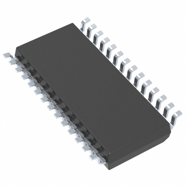
SO28 / SDIP32
Rev. 3
1/141
1
�Table of Contents
1 INTRODUCTION . . . . . . . . . . . . . . . . . . . . . . . . . . . . . . . . . . . . . . . . . . . . . . . . . . . . . . . . . . . . . . 6
2 PIN DESCRIPTION . . . . . . . . . . . . . . . . . . . . . . . . . . . . . . . . . . . . . . . . . . . . . . . . . . . . . . . . . . . . 7
3 REGISTER & MEMORY MAP . . . . . . . . . . . . . . . . . . . . . . . . . . . . . . . . . . . . . . . . . . . . . . . . . . . 10
4 FLASH PROGRAM MEMORY . . . . . . . . . . . . . . . . . . . . . . . . . . . . . . . . . . . . . . . . . . . . . . . . . . 13
4.1 INTRODUCTION . . . . . . . . . . . . . . . . . . . . . . . . . . . . . . . . . . . . . . . . . . . . . . . . . . . . . . . 13
4.2
MAIN FEATURES . . . . . . . . . . . . . . . . . . . . . . . . . . . . . . . . . . . . . . . . . . . . . . . . . . . . . . 13
4.3
STRUCTURAL ORGANISATION . . . . . . . . . . . . . . . . . . . . . . . . . . . . . . . . . . . . . . . . . . 13
4.4
IN-SITU PROGRAMMING (ISP) MODE . . . . . . . . . . . . . . . . . . . . . . . . . . . . . . . . . . . . . 13
4.5
MEMORY READ-OUT PROTECTION . . . . . . . . . . . . . . . . . . . . . . . . . . . . . . . . . . . . . . 13
5 CENTRAL PROCESSING UNIT . . . . . . . . . . . . . . . . . . . . . . . . . . . . . . . . . . . . . . . . . . . . . . . . . 14
5.1 INTRODUCTION . . . . . . . . . . . . . . . . . . . . . . . . . . . . . . . . . . . . . . . . . . . . . . . . . . . . . . . 14
c
u
d
5.2
MAIN FEATURES . . . . . . . . . . . . . . . . . . . . . . . . . . . . . . . . . . . . . . . . . . . . . . . . . . . . . . 14
5.3
CPU REGISTERS . . . . . . . . . . . . . . . . . . . . . . . . . . . . . . . . . . . . . . . . . . . . . . . . . . . . . . 14
o
r
P
6 SUPPLY, RESET AND CLOCK MANAGEMENT . . . . . . . . . . . . . . . . . . . . . . . . . . . . . . . . . . . . 17
6.1 LOW VOLTAGE DETECTOR (LVD) . . . . . . . . . . . . . . . . . . . . . . . . . . . . . . . . . . . . . . . . 18
6.2
e
t
le
RESET SEQUENCE MANAGER (RSM) . . . . . . . . . . . . . . . . . . . . . . . . . . . . . . . . . . . . . 19
6.2.1
Introduction . . . . . . . . . . . . . . . . . . . . . . . . . . . . . . . . . . . . . . . . . . . . . . . . . . . . . .
6.2.2
Asynchronous External RESET pin . . . . . . . . . . . . . . . . . . . . . . . . . . . . . . . . . . .
6.2.3
Internal Low Voltage Detection RESET . . . . . . . . . . . . . . . . . . . . . . . . . . . . . . . .
6.2.4
Internal Watchdog RESET . . . . . . . . . . . . . . . . . . . . . . . . . . . . . . . . . . . . . . . . . .
6.3 MULTI-OSCILLATOR (MO) . . . . . . . . . . . . . . . . . . . . . . . . . . . . . . . . . . . . . . . . . . . . . . .
o
s
b
6.4
O
)
s
(
t
c
19
20
20
20
21
CLOCK SECURITY SYSTEM (CSS) . . . . . . . . . . . . . . . . . . . . . . . . . . . . . . . . . . . . . . . . 22
6.4.1
Clock Filter Control . . . . . . . . . . . . . . . . . . . . . . . . . . . . . . . . . . . . . . . . . . . . . . . .
6.4.2
Safe Oscillator Control . . . . . . . . . . . . . . . . . . . . . . . . . . . . . . . . . . . . . . . . . . . . .
6.4.3
Low Power Modes . . . . . . . . . . . . . . . . . . . . . . . . . . . . . . . . . . . . . . . . . . . . . . . .
6.4.4
Interrupts . . . . . . . . . . . . . . . . . . . . . . . . . . . . . . . . . . . . . . . . . . . . . . . . . . . . . . . .
6.5 CLOCK RESET AND SUPPLY REGISTER DESCRIPTION (CRSR) . . . . . . . . . . . . . . .
u
d
o
6.6
r
P
e
22
22
22
22
23
MAIN CLOCK CONTROLLER (MCC) . . . . . . . . . . . . . . . . . . . . . . . . . . . . . . . . . . . . . . . 24
t
e
l
o
7 INTERRUPTS . . . . . . . . . . . . . . . . . . . . . . . . . . . . . . . . . . . . . . . . . . . . . . . . . . . . . . . . . . . . . . . 25
7.1 NON-MASKABLE SOFTWARE INTERRUPT . . . . . . . . . . . . . . . . . . . . . . . . . . . . . . . . . 25
s
b
O
7.2
EXTERNAL INTERRUPTS . . . . . . . . . . . . . . . . . . . . . . . . . . . . . . . . . . . . . . . . . . . . . . . 25
7.3
PERIPHERAL INTERRUPTS . . . . . . . . . . . . . . . . . . . . . . . . . . . . . . . . . . . . . . . . . . . . . 25
8 POWER SAVING MODES . . . . . . . . . . . . . . . . . . . . . . . . . . . . . . . . . . . . . . . . . . . . . . . . . . . . . 27
8.1 INTRODUCTION . . . . . . . . . . . . . . . . . . . . . . . . . . . . . . . . . . . . . . . . . . . . . . . . . . . . . . . 27
8.2
SLOW MODE . . . . . . . . . . . . . . . . . . . . . . . . . . . . . . . . . . . . . . . . . . . . . . . . . . . . . . . . . 27
8.3
WAIT MODE . . . . . . . . . . . . . . . . . . . . . . . . . . . . . . . . . . . . . . . . . . . . . . . . . . . . . . . . . . 28
8.4
HALT MODE . . . . . . . . . . . . . . . . . . . . . . . . . . . . . . . . . . . . . . . . . . . . . . . . . . . . . . . . . . 29
9 I/O PORTS . . . . . . . . . . . . . . . . . . . . . . . . . . . . . . . . . . . . . . . . . . . . . . . . . . . . . . . . . . . . . . . . . . 30
9.1 INTRODUCTION . . . . . . . . . . . . . . . . . . . . . . . . . . . . . . . . . . . . . . . . . . . . . . . . . . . . . . . 30
9.2
FUNCTIONAL DESCRIPTION . . . . . . . . . . . . . . . . . . . . . . . . . . . . . . . . . . . . . . . . . . . . 30
9.2.1
Input Modes . . . . . . . . . . . . . . . . . . . . . . . . . . . . . . . . . . . . . . . . . . . . . . . . . . . . .
9.2.2
Output Modes . . . . . . . . . . . . . . . . . . . . . . . . . . . . . . . . . . . . . . . . . . . . . . . . 141
....
9.2.3
Alternate Functions . . . . . . . . . . . . . . . . . . . . . . . . . . . . . . . . . . . . . . . . . . . . . . . .
9.3 I/O PORT IMPLEMENTATION . . . . . . . . . . . . . . . . . . . . . . . . . . . . . . . . . . . . . . . . . . . .
2/141
2
)
s
t(
30
30
30
33
�Table of Contents
9.4
LOW POWER MODES . . . . . . . . . . . . . . . . . . . . . . . . . . . . . . . . . . . . . . . . . . . . . . . . . . 34
9.5
INTERRUPTS . . . . . . . . . . . . . . . . . . . . . . . . . . . . . . . . . . . . . . . . . . . . . . . . . . . . . . . . . 34
9.6
REGISTER DESCRIPTION . . . . . . . . . . . . . . . . . . . . . . . . . . . . . . . . . . . . . . . . . . . . . . . 34
10 MISCELLANEOUS REGISTERS . . . . . . . . . . . . . . . . . . . . . . . . . . . . . . . . . . . . . . . . . . . . . . . 36
10.1 I/O PORT INTERRUPT SENSITIVITY . . . . . . . . . . . . . . . . . . . . . . . . . . . . . . . . . . . . . . 36
10.2 I/O PORT ALTERNATE FUNCTIONS . . . . . . . . . . . . . . . . . . . . . . . . . . . . . . . . . . . . . . . 36
10.3 MISCELLANEOUS REGISTER DESCRIPTION . . . . . . . . . . . . . . . . . . . . . . . . . . . . . . . 37
11 ON-CHIP PERIPHERALS . . . . . . . . . . . . . . . . . . . . . . . . . . . . . . . . . . . . . . . . . . . . . . . . . . . . . 39
11.1 WATCHDOG TIMER (WDG) . . . . . . . . . . . . . . . . . . . . . . . . . . . . . . . . . . . . . . . . . . . . . . 39
11.1.1 Introduction . . . . . . . . . . . . . . . . . . . . . . . . . . . . . . . . . . . . . . . . . . . . . . . . . . . . . .
11.1.2 Main Features . . . . . . . . . . . . . . . . . . . . . . . . . . . . . . . . . . . . . . . . . . . . . . . . . . . .
11.1.3 Functional Description . . . . . . . . . . . . . . . . . . . . . . . . . . . . . . . . . . . . . . . . . . . . .
11.1.4 Hardware Watchdog Option . . . . . . . . . . . . . . . . . . . . . . . . . . . . . . . . . . . . . . . . .
11.1.5 Low Power Modes . . . . . . . . . . . . . . . . . . . . . . . . . . . . . . . . . . . . . . . . . . . . . . . .
11.1.6 Interrupts . . . . . . . . . . . . . . . . . . . . . . . . . . . . . . . . . . . . . . . . . . . . . . . . . . . . . . . .
11.1.7 Register Description . . . . . . . . . . . . . . . . . . . . . . . . . . . . . . . . . . . . . . . . . . . . . . .
11.2 16-BIT TIMER . . . . . . . . . . . . . . . . . . . . . . . . . . . . . . . . . . . . . . . . . . . . . . . . . . . . . . . . .
39
39
39
40
40
40
40
42
11.2.1 Introduction . . . . . . . . . . . . . . . . . . . . . . . . . . . . . . . . . . . . . . . . . . . . . . . . . . . . . .
11.2.2 Main Features . . . . . . . . . . . . . . . . . . . . . . . . . . . . . . . . . . . . . . . . . . . . . . . . . . . .
11.2.3 Functional Description . . . . . . . . . . . . . . . . . . . . . . . . . . . . . . . . . . . . . . . . . . . . .
11.2.4 Low Power Modes . . . . . . . . . . . . . . . . . . . . . . . . . . . . . . . . . . . . . . . . . . . . . . . .
11.2.5 Interrupts . . . . . . . . . . . . . . . . . . . . . . . . . . . . . . . . . . . . . . . . . . . . . . . . . . . . . . .
11.2.6 Summary of Timer modes . . . . . . . . . . . . . . . . . . . . . . . . . . . . . . . . . . . . . . . . . .
11.2.7 Register Description . . . . . . . . . . . . . . . . . . . . . . . . . . . . . . . . . . . . . . . . . . . . . . .
11.3 SERIAL PERIPHERAL INTERFACE (SPI) . . . . . . . . . . . . . . . . . . . . . . . . . . . . . . . . . . .
42
42
42
54
54
54
55
60
11.3.1 Introduction . . . . . . . . . . . . . . . . . . . . . . . . . . . . . . . . . . . . . . . . . . . . . . . . . . . . . .
11.3.2 Main Features . . . . . . . . . . . . . . . . . . . . . . . . . . . . . . . . . . . . . . . . . . . . . . . . . . . .
11.3.3 General description . . . . . . . . . . . . . . . . . . . . . . . . . . . . . . . . . . . . . . . . . . . . . . . .
11.3.4 Functional Description . . . . . . . . . . . . . . . . . . . . . . . . . . . . . . . . . . . . . . . . . . . . .
11.3.5 Low Power Modes . . . . . . . . . . . . . . . . . . . . . . . . . . . . . . . . . . . . . . . . . . . . . . . .
11.3.6 Interrupts . . . . . . . . . . . . . . . . . . . . . . . . . . . . . . . . . . . . . . . . . . . . . . . . . . . . . . .
11.3.7 Register Description . . . . . . . . . . . . . . . . . . . . . . . . . . . . . . . . . . . . . . . . . . . . . . .
11.4 I2C BUS INTERFACE (I2C) . . . . . . . . . . . . . . . . . . . . . . . . . . . . . . . . . . . . . . . . . . . . . .
60
60
60
62
69
69
70
73
11.4.1 Introduction . . . . . . . . . . . . . . . . . . . . . . . . . . . . . . . . . . . . . . . . . . . . . . . . . . . . . .
11.4.2 Main Features . . . . . . . . . . . . . . . . . . . . . . . . . . . . . . . . . . . . . . . . . . . . . . . . . . . .
11.4.3 General Description . . . . . . . . . . . . . . . . . . . . . . . . . . . . . . . . . . . . . . . . . . . . . . .
11.4.4 Functional Description . . . . . . . . . . . . . . . . . . . . . . . . . . . . . . . . . . . . . . . . . . . . .
11.4.5 Low Power Modes . . . . . . . . . . . . . . . . . . . . . . . . . . . . . . . . . . . . . . . . . . . . . . . .
11.4.6 Interrupts . . . . . . . . . . . . . . . . . . . . . . . . . . . . . . . . . . . . . . . . . . . . . . . . . . . . . . . .
11.4.7 Register Description . . . . . . . . . . . . . . . . . . . . . . . . . . . . . . . . . . . . . . . . . . . . . . .
11.5 8-BIT A/D CONVERTER (ADC) . . . . . . . . . . . . . . . . . . . . . . . . . . . . . . . . . . . . . . . . . . .
73
73
73
75
79
79
80
86
)
s
t(
c
u
d
e
t
le
o
r
P
so
)
s
(
ct
b
O
-
u
d
o
r
P
e
t
e
l
o
s
b
O
11.5.1
11.5.2
11.5.3
11.5.4
11.5.5
11.5.6
Introduction . . . . . . . . . . . . . . . . . . . . . . . . . . . . . . . . . . . . . . . . . . . . . . . . . . . . . .
Main Features . . . . . . . . . . . . . . . . . . . . . . . . . . . . . . . . . . . . . . . . . . . . . . . . . . . .
Functional Description . . . . . . . . . . . . . . . . . . . . . . . . . . . . . . . . . . . . . . . . . . . . .
Low Power Modes . . . . . . . . . . . . . . . . . . . . . . . . . . . . . . . . . . . . . . . . . . . . . . . .
Interrupts . . . . . . . . . . . . . . . . . . . . . . . . . . . . . . . . . . . . . . . . . . . . . . . . . . . . . . . .
Register Description . . . . . . . . . . . . . . . . . . . . . . . . . . . . . . . . . . . . . . . . . . . . . . .
86
86
86
87
87
88
3/141
3
�Table of Contents
12 INSTRUCTION SET . . . . . . . . . . . . . . . . . . . . . . . . . . . . . . . . . . . . . . . . . . . . . . . . . . . . . . . . . 90
12.1 ST7 ADDRESSING MODES . . . . . . . . . . . . . . . . . . . . . . . . . . . . . . . . . . . . . . . . . . . . . . 90
12.1.1 Inherent . . . . . . . . . . . . . . . . . . . . . . . . . . . . . . . . . . . . . . . . . . . . . . . . . . . . . . . . .
12.1.2 Immediate . . . . . . . . . . . . . . . . . . . . . . . . . . . . . . . . . . . . . . . . . . . . . . . . . . . . . . .
12.1.3 Direct . . . . . . . . . . . . . . . . . . . . . . . . . . . . . . . . . . . . . . . . . . . . . . . . . . . . . . . . . .
12.1.4 Indexed (No Offset, Short, Long) . . . . . . . . . . . . . . . . . . . . . . . . . . . . . . . . . . . . .
12.1.5 Indirect (Short, Long) . . . . . . . . . . . . . . . . . . . . . . . . . . . . . . . . . . . . . . . . . . . . . .
12.1.6 Indirect Indexed (Short, Long) . . . . . . . . . . . . . . . . . . . . . . . . . . . . . . . . . . . . . . .
12.1.7 Relative Mode (Direct, Indirect) . . . . . . . . . . . . . . . . . . . . . . . . . . . . . . . . . . . . . .
12.2 INSTRUCTION GROUPS . . . . . . . . . . . . . . . . . . . . . . . . . . . . . . . . . . . . . . . . . . . . . . . .
91
91
91
91
91
92
92
93
13 ELECTRICAL CHARACTERISTICS . . . . . . . . . . . . . . . . . . . . . . . . . . . . . . . . . . . . . . . . . . . . . 96
13.1 PARAMETER CONDITIONS . . . . . . . . . . . . . . . . . . . . . . . . . . . . . . . . . . . . . . . . . . . . . . 96
c
u
d
)
s
t(
13.1.1 Minimum and Maximum values . . . . . . . . . . . . . . . . . . . . . . . . . . . . . . . . . . . . . .
13.1.2 Typical values . . . . . . . . . . . . . . . . . . . . . . . . . . . . . . . . . . . . . . . . . . . . . . . . . . . .
13.1.3 Typical curves . . . . . . . . . . . . . . . . . . . . . . . . . . . . . . . . . . . . . . . . . . . . . . . . . . . .
13.1.4 Loading capacitor . . . . . . . . . . . . . . . . . . . . . . . . . . . . . . . . . . . . . . . . . . . . . . . . .
13.1.5 Pin input voltage . . . . . . . . . . . . . . . . . . . . . . . . . . . . . . . . . . . . . . . . . . . . . . . . . .
13.2 ABSOLUTE MAXIMUM RATINGS . . . . . . . . . . . . . . . . . . . . . . . . . . . . . . . . . . . . . . . . .
e
t
le
o
r
P
so
13.2.1 Voltage Characteristics . . . . . . . . . . . . . . . . . . . . . . . . . . . . . . . . . . . . . . . . . . . .
13.2.2 Current Characteristics . . . . . . . . . . . . . . . . . . . . . . . . . . . . . . . . . . . . . . . . . . . .
13.2.3 Thermal Characteristics . . . . . . . . . . . . . . . . . . . . . . . . . . . . . . . . . . . . . . . . . . . .
13.3 OPERATING CONDITIONS . . . . . . . . . . . . . . . . . . . . . . . . . . . . . . . . . . . . . . . . . . . . . .
)
s
(
ct
b
O
-
96
96
96
96
96
97
97
97
97
98
13.3.1 General Operating Conditions . . . . . . . . . . . . . . . . . . . . . . . . . . . . . . . . . . . . . . . 98
13.3.2 Operating Conditions with Low Voltage Detector (LVD) . . . . . . . . . . . . . . . . . . . 100
13.4 SUPPLY CURRENT CHARACTERISTICS . . . . . . . . . . . . . . . . . . . . . . . . . . . . . . . . . . 102
du
13.4.1 RUN and SLOW Modes . . . . . . . . . . . . . . . . . . . . . . . . . . . . . . . . . . . . . . . . . . .
13.4.2 WAIT and SLOW WAIT Modes . . . . . . . . . . . . . . . . . . . . . . . . . . . . . . . . . . . . .
13.4.3 HALT Mode . . . . . . . . . . . . . . . . . . . . . . . . . . . . . . . . . . . . . . . . . . . . . . . . . . . .
13.4.4 Supply and Clock Managers . . . . . . . . . . . . . . . . . . . . . . . . . . . . . . . . . . . . . . . .
13.4.5 On-Chip Peripherals . . . . . . . . . . . . . . . . . . . . . . . . . . . . . . . . . . . . . . . . . . . . .
13.5 CLOCK AND TIMING CHARACTERISTICS . . . . . . . . . . . . . . . . . . . . . . . . . . . . . . . . .
102
103
104
104
104
105
13.5.1 General Timings . . . . . . . . . . . . . . . . . . . . . . . . . . . . . . . . . . . . . . . . . . . . . . . .
13.5.2 External Clock Source . . . . . . . . . . . . . . . . . . . . . . . . . . . . . . . . . . . . . . . . . . . .
13.5.3 Crystal and Ceramic Resonator Oscillators . . . . . . . . . . . . . . . . . . . . . . . . . . . .
13.5.4 RC Oscillators . . . . . . . . . . . . . . . . . . . . . . . . . . . . . . . . . . . . . . . . . . . . . . . . . . .
13.5.5 Clock Security System (CSS) . . . . . . . . . . . . . . . . . . . . . . . . . . . . . . . . . . . . . .
13.6 MEMORY CHARACTERISTICS . . . . . . . . . . . . . . . . . . . . . . . . . . . . . . . . . . . . . . . . . .
105
105
106
110
111
112
e
t
e
ol
o
r
P
s
b
O
13.6.1 RAM and Hardware Registers . . . . . . . . . . . . . . . . . . . . . . . . . . . . . . . . . . . . . . 112
13.6.2 FLASH Program Memory . . . . . . . . . . . . . . . . . . . . . . . . . . . . . . . . . . . . . . . . . 112
13.7 EMC CHARACTERISTICS . . . . . . . . . . . . . . . . . . . . . . . . . . . . . . . . . . . . . . . . . . . . . . 113
13.7.1 Functional EMS . . . . . . . . . . . . . . . . . . . . . . . . . . . . . . . . . . . . . . . . . . . . . . . . .
13.7.2 Absolute Electrical Sensitivity . . . . . . . . . . . . . . . . . . . . . . . . . . . . . . . . . . . . . . .
13.7.3 ESD Pin Protection Strategy . . . . . . . . . . . . . . . . . . . . . . . . . . . . . . . . . . . . . . . .
13.8 I/O PORT PIN CHARACTERISTICS . . . . . . . . . . . . . . . . . . . . . . . . . . . . . . . . . . . . . . .
113
114
116
118
13.8.1 General Characteristics . . . . . . . . . . . . . . . . . . . . . . . . . . . . . . . . . . . . . . . . 141
. . . 118
13.8.2 Output Driving Current . . . . . . . . . . . . . . . . . . . . . . . . . . . . . . . . . . . . . . . . . . . . 119
13.9 CONTROL PIN CHARACTERISTICS . . . . . . . . . . . . . . . . . . . . . . . . . . . . . . . . . . . . . . 121
4/141
�Table of Contents
13.9.1 Asynchronous RESET Pin . . . . . . . . . . . . . . . . . . . . . . . . . . . . . . . . . . . . . . . . . 121
13.9.2 ISPSEL Pin . . . . . . . . . . . . . . . . . . . . . . . . . . . . . . . . . . . . . . . . . . . . . . . . . . . . . 123
13.10 TIMER PERIPHERAL CHARACTERISTICS . . . . . . . . . . . . . . . . . . . . . . . . . . . . . . . . . 124
13.10.1 Watchdog Timer . . . . . . . . . . . . . . . . . . . . . . . . . . . . . . . . . . . . . . . . . . . . . . . . 124
13.10.2 16-Bit Timer . . . . . . . . . . . . . . . . . . . . . . . . . . . . . . . . . . . . . . . . . . . . . . . . . . . . 124
13.11 COMMUNICATION INTERFACE CHARACTERISTICS . . . . . . . . . . . . . . . . . . . . . . . . 125
13.11.1 SPI - Serial Peripheral Interface . . . . . . . . . . . . . . . . . . . . . . . . . . . . . . . . . . . . . 125
13.11.2 I2C - Inter IC Control Interface . . . . . . . . . . . . . . . . . . . . . . . . . . . . . . . . . . . . . . 127
13.12 8-BIT ADC CHARACTERISTICS . . . . . . . . . . . . . . . . . . . . . . . . . . . . . . . . . . . . . . . . . 128
)
s
t(
14 PACKAGE CHARACTERISTICS . . . . . . . . . . . . . . . . . . . . . . . . . . . . . . . . . . . . . . . . . . . . . . 130
14.1 PACKAGE MECHANICAL DATA . . . . . . . . . . . . . . . . . . . . . . . . . . . . . . . . . . . . . . . . . 130
c
u
d
14.2 THERMAL CHARACTERISTICS . . . . . . . . . . . . . . . . . . . . . . . . . . . . . . . . . . . . . . . . . 131
14.3 SOLDERING INFORMATION . . . . . . . . . . . . . . . . . . . . . . . . . . . . . . . . . . . . . . . . . . . . 132
o
r
P
15 DEVICE CONFIGURATION AND ORDERING INFORMATION . . . . . . . . . . . . . . . . . . . . . . . 133
15.1 OPTION BYTES . . . . . . . . . . . . . . . . . . . . . . . . . . . . . . . . . . . . . . . . . . . . . . . . . . . . . . 133
15.2 DEVICE ORDERING INFORMATION AND TRANSFER OF CUSTOMER CODE . . . . 134
e
t
le
15.3 DEVELOPMENT TOOLS . . . . . . . . . . . . . . . . . . . . . . . . . . . . . . . . . . . . . . . . . . . . . . . 136
o
s
b
15.3.1 PACKAGE/SOCKET FOOTPRINT PROPOSAL . . . . . . . . . . . . . . . . . . . . . . . . 137
15.4 ST7 APPLICATION NOTES . . . . . . . . . . . . . . . . . . . . . . . . . . . . . . . . . . . . . . . . . . . . . 138
16 SUMMARY OF CHANGES . . . . . . . . . . . . . . . . . . . . . . . . . . . . . . . . . . . . . . . . . . . . . . . . . . . 140
O
)
s
(
t
c
u
d
o
r
P
e
t
e
l
o
s
b
O
5/141
�ST72104Gx, ST72215Gx, ST72216Gx, ST72254Gx
1 INTRODUCTION
The ST72104G, ST72215G, ST72216G and
ST72254G devices are members of the ST7 microcontroller family. They can be grouped as follows:
– ST72254G devices are designed for mid-range
applications with ADC and I²C interface capabilities.
– ST72215/6G devices target the same range of
applications but without I²C interface.
– ST72104G devices are for applications that do
not need ADC and I²C peripherals.
All devices are based on a common industrystandard 8-bit core, featuring an enhanced instruction set.
The ST72C104G, ST72C215G, ST72C216G and
ST72C254G versions feature single-voltage
FLASH memory with byte-by-byte In-Situ Programming (ISP) capability.
Under software control, all devices can be placed
in WAIT, SLOW, or HALT mode, reducing power
consumption when the application is in idle or
stand-by state.
The enhanced instruction set and addressing
modes of the ST7 offer both power and flexibility to
software developers, enabling the design of highly
efficient and compact application code. In addition
to standard 8-bit data management, all ST7 microcontrollers feature true bit manipulation, 8x8 unsigned multiplication and indirect addressing
modes.
For easy reference, all parametric data are located
in Section 13 on page 96.
)
s
t(
c
u
d
e
t
le
o
s
b
Figure 1. General Block Diagram
OSC1
OSC2
MULTI OSC
+
CLOCK FILTER
VSS
s
b
O
Pr
CONTROL
8-BIT CORE
ALU
PROGRAM
MEMORY
(4 or 8K Bytes)
4
I2C
PORT A
PA7:0
(8 bits)
SPI
POWER
SUPPLY
RAM
(256 Bytes)
6/141
s
(
t
c
ADDRESS AND DATA BUS
e
t
e
ol
RESET
O
)
Internal
CLOCK
u
d
o
LVD
VDD
o
r
P
PORT B
PB7:0
(8 bits)
16-BIT TIMER A
PORT C
8-BIT ADC
16-BIT TIMER B
WATCHDOG
PC5:0
(6 bits)
�ST72104Gx, ST72215Gx, ST72216Gx, ST72254Gx
2 PIN DESCRIPTION
Figure 2. 28-Pin SO Package Pinout
RESET
1
28
VDD
OSC1
OSC2
2
27
3
26
VSS
ISPSEL
SS/PB7
4
25
PA0 (HS)
ISPCLK/SCK/PB6
5
24
PA1 (HS)
ISPDATA/MISO/PB5
6
23
PA2 (HS)
MOSI/PB4
7
22
PA3 (HS)
21
PA4 (HS)/SCLI
ei1
ei0
OCMP2_A/PB3
8
ICAP2_A/PB2
9
20
PA5 (HS)
OCMP1_A/PB1
ICAP1_A/PB0
10
19
11
18
PA6 (HS)/SDAI
PA7 (HS)
AIN5/EXTCLK_A/PC5
AIN4/OCMP2_B/PC4
12
17
AIN3/ICAP2_B/PC3
14
13
ei0 or ei1
RESET
ro
Ob
15
PC2/MCO/AIN2
o
s
b
(HS) 20mA high sink capability
eiX associated external interrupt vector
1
32
VDD
2
31
VSS
ISPSEL
PA0 (HS)
PA1 (HS)
3
30
SS/PB7
4
29
ISPCLK/SCK/PB6
5
ISPDATA/MISO/PB5
MOSI/PB4
NC
6
27
7
26
8
25
NC
OCMP2_A/PB3
ICAP2_A/PB2
9
24
10
23
NC
NC
PA4 (HS)/SCLI
22
PA5 (HS)
OCMP1_A/PB1
12
21
ICAP1_A/PB0
13
AIN5/EXTCLK_A/PC5
AIN4/OCMP2_B/PC4
14
18
PA6 (HS)/SDAI
PA7 (HS)
PC0/ICAP1_B/AIN0
PC1/OCMP1_B/AIN1
AIN3/ICAP2_B/PC3
16
17
PC2/MCO/AIN2
P
e
let
so
s
(
t
c
du
OSC1
OSC2
16
e
t
le
11
15
ei1
ei1
ei0
ei0
28
20
19
ei0 or ei1
c
u
d
o
r
P
PC0/ICAP1_B/AIN0
PC1/OCMP1_B/AIN1
O
)
Figure 3. 32-Pin SDIP Package Pinout
)
s
t(
PA2 (HS)
PA3 (HS)
(HS) 20mA high sink capability
eiX associated external interrupt vector
7/141
5
�ST72104Gx, ST72215Gx, ST72216Gx, ST72254Gx
PIN DESCRIPTION (Cont’d)
For external pin connection guidelines, refer to Section 13 "ELECTRICAL CHARACTERISTICS" on page
96.
Legend / Abbreviations for Table 1:
Type:
I = input, O = output, S = supply
Input level:
A = Dedicated analog input
In/Output level: C = CMOS 0.3VDD/0.7VDD,
CT= CMOS 0.3VDD/0.7VDD with input trigger
Output level:
HS = 20mA high sink (on N-buffer only)
Port and control configuration:
– Input:
float = floating, wpu = weak pull-up, int = interrupt 1), ana = analog
– Output:
OD = open drain 2), PP = push-pull
Refer to Section 9 "I/O PORTS" on page 30 for more details on the software configuration of the I/O ports.
The RESET configuration of each pin is shown in bold. This configuration is valid as long as the device is
in reset state.
)
s
t(
c
u
d
e
t
le
Table 1. Device Pin Description
Port / Control
ana
PP
OD
int
O
)
Alternate Function
2
2 OSC1 3)
I
3
3 OSC2 3)
O
4
4 PB7/SS
5
5 PB6/SCK/ISPCLK
6
6 PB5/MISO/ISPDATA
7
7 PB4/MOSI
8
10
Ob
8 PB3/OCMP2_A
I/O
CT
X
ei1
X
X
Port B3
Timer A Output Compare 2
11
9 PB2/ICAP2_A
I/O
CT
X
ei1
X
X
Port B2
Timer A Input Capture 2
12 10 PB1 /OCMP1_A
I/O
CT
X
ei1
X
X
Port B1
Timer A Output Compare 1
13 11 PB0 /ICAP1_A
I/O
CT
X
ei1
X
X
Port B0
Timer A Input Capture 1
14 12 PC5/EXTCLK_A/AIN5 I/O
CT
X ei0/ei1
X
X
Port C5
15 13 PC4/OCMP2_B/AIN4
I/O
CT
X ei0/ei1
X
X
Port C4
16 14 PC3/ ICAP2_B/AIN3
I/O
CT
X ei0/ei1 X
X
X
Port C3
17 15 PC2/MCO/AIN2
I/O
CT
X ei0/ei1 X
X
X
Port C2
9
8/141
6
u
d
o
Top priority non maskable interrupt (active low)
External clock input or Resonator oscillator inverter input or resistor input for RC oscillator
Resonator oscillator inverter output or capacitor input for RC oscillator
Pr
CT
X
ei1
X
X
Port B7
SPI Slave Select (active low)
CT
X
ei1
X
X
Port B6
SPI Serial Clock or ISP Clock
I/O
CT
X
ei1
X
X
Port B5
SPI Master In/ Slave Out Data
or ISP Data
I/O
CT
X
ei1
X
X
Port B4
SPI Master Out / Slave In Data
I/O
so
s
(
t
c
X
Main
Function
(after reset)
1 RESET
e
t
e
l
X
o
s
b
Output
1
NC
I/O CT
wpu
Input
float
Output
Input
Pin Name
Type
Level
SO28
SDIP32
Pin n°
o
r
P
I/O
Not Connected
NC
Timer A Input Clock or ADC
Analog Input 5
Timer B Output Compare 2 or
ADC Analog Input 4
Timer B Input Capture 2 or
ADC Analog Input 3
Main clock output (fCPU) or
ADC Analog Input 2
�ST72104Gx, ST72215Gx, ST72216Gx, ST72254Gx
Port / Control
Main
Function
(after reset)
PP
18 16 PC1/OCMP1_B/AIN1
I/O
CT
X ei0/ei1 X
X
X
Port C1
19 17 PC0/ICAP1_B/AIN0
I/O
CT
X ei0/ei1 X
X
X
Port C0
20 18 PA7
I/O CT HS
X
X
X
Port A7
21 19 PA6 /SDAI
I/O CT HS
X
22 20 PA5
I/O CT HS
X
23 21 PA4 /SCLI
I/O CT HS
X
24
NC
25
NC
int
OD
Output
ana
wpu
Input
float
Output
Pin Name
Input
Type
Level
SO28
SDIP32
Pin n°
ei0
ei0
ei0
ei0
T
X
Timer B Output Compare 1 or
ADC Analog Input 1
Timer B Input Capture 1 or
ADC Analog Input 0
Port A5
T
Not Connected
I/O CT HS
X
ei0
X
X
Port A3
27 23 PA2
I/O CT HS
X
ei0
X
X
Port A2
28 24 PA1
I/O CT HS
X
ei0
X
X
29 25 PA0
I/O CT HS
X
ei0
X
X
30 26 ISPSEL
I
31 27 VSS
S
32 28 VDD
S
C
X
u
d
o
ct
(s)
c
u
d
I2C Clock
Port A4
26 22 PA3
)
s
t(
I2C Data
Port A6
X
Alternate Function
e
t
le
o
r
P
-O
o
s
b
Port A1
Port A0
In situ programming selection (Should be tied
low in standard user mode).
Ground
Main power supply
Notes:
1. In the interrupt input column, “eiX” defines the associated external interrupt vector. If the weak pull-up
column (wpu) is merged with the interrupt column (int), then the I/O configuration is pull-up interrupt input,
else the configuration is floating interrupt input.
2. In the open drain output column, “T” defines a true open drain I/O (P-Buffer and protection diode to VDD
are not implemented). See Section 9 "I/O PORTS" on page 30 and Section 13.8 "I/O PORT PIN CHARACTERISTICS" on page 118 for more details.
3. OSC1 and OSC2 pins connect a crystal or ceramic resonator, an external RC, or an external source to
the on-chip oscillator see Section 2 "PIN DESCRIPTION" on page 7 and Section 13.5 "CLOCK AND TIMING CHARACTERISTICS" on page 105 for more details.
r
P
e
t
e
l
o
s
b
O
9/141
�ST72104Gx, ST72215Gx, ST72216Gx, ST72254Gx
3 REGISTER & MEMORY MAP
As shown in the Figure 4, the MCU is capable of
addressing 64K bytes of memories and I/O registers.
The available memory locations consist of 128
bytes of register location, 256 bytes of RAM and
up to 8Kbytes of user program memory. The RAM
space includes up to 128 bytes for the stack from
0100h to 017Fh.
The highest address bytes contain the user reset
and interrupt vectors.
IMPORTANT: Memory locations marked as “Reserved” must never be accessed. Accessing a reserved area can have unpredictable effects on the
device.
)
s
t(
Figure 4. Memory Map
0000h
c
u
d
HW Registers
(see Table 2)
0080h
256 Bytes RAM
00FFh
0100h
007Fh
0080h
FFFFh
s
b
O
10/141
)
s
(
ct
du
Interrupt & Reset Vectors
(see Table 5 on page 26)
e
t
e
ol
-O
017Fh
Reserved
DFFFh
E000h
FFDFh
FFE0h
o
r
P
e
t
le
o
s
b
017Fh
0180h
Program Memory
(4K, 8 KBytes)
o
r
P
Short Addressing RAM
Zero page
(128 Bytes)
Stack or
16-bit Addressing RAM
(128 Bytes)
E000h
8 KBytes
F000h
4 KBytes
FFFFh
�ST72104Gx, ST72215Gx, ST72216Gx, ST72254Gx
Table 2. Hardware Register Map
Address
Register
Label
Block
0000h
0001h
0002h
Port C
PCDR
PCDDR
PCOR
Register Name
Reset
Status
Port C Data Register
Port C Data Direction Register
Port C Option Register
00h 1)
00h
00h
R/W 2)
R/W 2)
R/W 2)
00h 1)
00h
00h
R/W
R/W
R/W.
0003h
Reserved (1 Byte)
0004h
0005h
0006h
Port B
PBDR
PBDDR
PBOR
Port B Data Register
Port B Data Direction Register
Port B Option Register
0007h
Port A
PADR
PADDR
PAOR
000Bh
to
001Fh
e
t
le
Reserved (21 Bytes)
0020h
0021h
0022h
0023h
SPI
0024h
WATCHDOG
0025h
MISCR1
Miscellaneous Register 1
SPIDR
SPICR
SPISR
SPI Data I/O Register
SPI Control Register
SPI Status Register
WDGCR
s
b
O
e
t
e
ol
I 2C
Pr
I2CCR
I2CSR1
I2CSR2
I2CCCR
I2COAR1
I2COAR2
I2CDR
o
s
b
o
r
P
R/W
R/W
R/W
00h
R/W
-O
xxh
0xh
00h
R/W
R/W
Read Only
Watchdog Control Register
7Fh
R/W
)
s
(
ct
u
d
o
CRSR
0026h
0027h
002Fh
to
0030h
00h 1)
00h
00h
Port A Data Register
Port A Data Direction Register
Port A Option Register
)
s
t(
c
u
d
Reserved (1 Byte)
0008h
0009h
000Ah
0028h
0029h
002Ah
002Bh
002Ch
002Dh
002Eh
Remarks
Clock, Reset, Supply Control / Status Register 000x 000x R/W
Reserved (2 bytes)
Control Register
Status Register 1
Status Register 2
Clock Control Register
Own Address Register 1
Own Address Register 2
Data Register
00h
00h
00h
00h
00h
00h
00h
R/W
Read Only
Read Only
R/W
R/W
R/W
R/W
Reserved (2 Bytes)
11/141
�ST72104Gx, ST72215Gx, ST72216Gx, ST72254Gx
Address
0031h
0032h
0033h
0034h
0035h
0036h
0037h
0038h
0039h
003Ah
003Bh
003Ch
003Dh
003Eh
003Fh
Register
Label
Block
Reset
Status
Register Name
TACR2
TACR1
TASR
TAIC1HR
TAIC1LR
TAOC1HR
TAOC1LR
TACHR
TACLR
TAACHR
TAACLR
TAIC2HR
TAIC2LR
TAOC2HR
TAOC2LR
Timer A Control Register 2
Timer A Control Register 1
Timer A Status Register
Timer A Input Capture 1 High Register
Timer A Input Capture 1 Low Register
Timer A Output Compare 1 High Register
Timer A Output Compare 1 Low Register
Timer A Counter High Register
Timer A Counter Low Register
Timer A Alternate Counter High Register
Timer A Alternate Counter Low Register
Timer A Input Capture 2 High Register
Timer A Input Capture 2 Low Register
Timer A Output Compare 2 High Register
Timer A Output Compare 2 Low Register
0040h
MISCR2
Miscellaneous Register 2
0041h
0042h
0043h
0044h
0045h
0046h
0047h
0048h
0049h
004Ah
004Bh
004Ch
004Dh
004Eh
004Fh
TBCR2
TBCR1
TBSR
TBIC1HR
TBIC1LR
TBOC1HR
TBOC1LR
TBCHR
TBCLR
TBACHR
TBACLR
TBIC2HR
TBIC2LR
TBOC2HR
TBOC2LR
Timer B Control Register 2
Timer B Control Register 1
Timer B Status Register
Timer B Input Capture 1 High Register
Timer B Input Capture 1 Low Register
Timer B Output Compare 1 High Register
Timer B Output Compare 1 Low Register
Timer B Counter High Register
Timer B Counter Low Register
Timer B Alternate Counter High Register
Timer B Alternate Counter Low Register
Timer B Input Capture 2 High Register
Timer B Input Capture 2 Low Register
Timer B Output Compare 2 High Register
Timer B Output Compare 2 Low Register
0050h
to
006Fh
TIMER A
TIMER B
0072h
to
007Fh
O
)
s
(
t
c
u
d
o
r
P
e
t
e
l
o
s
b
O
0070h
0071h
o
s
b
ADC
ADCDR
ADCCSR
e
t
le
Remarks
00h
00h
xxh
xxh
xxh
80h
00h
FFh
FCh
FFh
FCh
xxh
xxh
80h
00h
c
u
d
00h
R/W
00h
00h
xxh
xxh
xxh
80h
00h
FFh
FCh
FFh
FCh
xxh
xxh
80h
00h
R/W
R/W
Read Only
Read Only
Read Only
R/W
R/W
Read Only
Read Only
Read Only
Read Only
Read Only
Read Only
R/W
R/W
00h
00h
Read Only
R/W
o
r
P
R/W
R/W
Read Only
Read Only
Read Only
R/W
R/W
Read Only
Read Only
Read Only
Read Only
Read Only
Read Only
R/W
R/W
)
s
t(
Reserved (32 Bytes)
Data Register
Control/Status Register
Reserved (14 Bytes)
Legend: x=undefined, R/W=read/write
Notes:
1. The contents of the I/O port DR registers are readable only in output configuration. In input configuration, the values of the I/O pins are returned instead of the DR register contents.
2. The bits associated with unavailable pins must always keep their reset value.
12/141
�ST72104Gx, ST72215Gx, ST72216Gx, ST72254Gx
4 FLASH PROGRAM MEMORY
■
■
■
■
Remote In-Situ Programming (ISP) mode
Up to 16 bytes programmed in the same cycle
MTP memory (Multiple Time Programmable)
Read-out memory protection against piracy
4.3 STRUCTURAL ORGANISATION
The FLASH program memory is organised in a
single 8-bit wide memory block which can be used
for storing both code and data constants.
The FLASH program memory is mapped in the upper part of the ST7 addressing space and includes
the reset and interrupt user vector area .
4.4 IN-SITU PROGRAMMING (ISP) MODE
)
s
(
ct
The FLASH program memory can be programmed
using Remote ISP mode. This ISP mode allows
the contents of the ST7 program memory to be updated using a standard ST7 programming tools after the device is mounted on the application board.
This feature can be implemented with a minimum
number of added components and board area impact.
An example Remote ISP hardware interface to the
standard ST7 programming tool is described below. For more details on ISP programming, refer to
the ST7 Programming Specification.
du
ete
o
r
P
ol
s
b
O
Remote ISP Overview
The Remote ISP mode is initiated by a specific sequence on the dedicated ISPSEL pin.
The Remote ISP is performed in three steps:
– Selection of the RAM execution mode
– Download of Remote ISP code in RAM
– Execution of Remote ISP code in RAM to program the user program into the FLASH
Remote ISP hardware configuration
In Remote ISP mode, the ST7 has to be supplied
with power (VDD and VSS) and a clock signal (oscillator and application crystal circuit for example).
)
s
t(
c
u
d
so
b
O
XTAL
CL0
e
t
le
o
r
P
HE10 CONNECTOR TYPE
TO PROGRAMMING TOOL
1
CL1
VDD
4.2 MAIN FEATURES
OSC1
FLASH devices have a single voltage non-volatile
FLASH memory that may be programmed in-situ
(or plugged in a programming tool) on a byte-bybyte basis.
This mode needs five signals (plus the VDD signal
if necessary) to be connected to the programming
tool. This signals are:
– RESET: device reset
– VSS: device ground power supply
– ISPCLK: ISP output serial clock pin
– ISPDATA: ISP input serial data pin
– ISPSEL: Remote ISP mode selection. This pin
must be connected to VSS on the application
board through a pull-down resistor.
If any of these pins are used for other purposes on
the application, a serial resistor has to be implemented to avoid a conflict if the other device forces
the signal level.
Figure 5 shows a typical hardware interface to a
standard ST7 programming tool. For more details
on the pin locations, refer to the device pinout description.
Figure 5. Typical Remote ISP Interface
OSC2
4.1 INTRODUCTION
ISPSEL
10KΩ
VSS
RESET
ST7
ISPCLK
ISPDATA
47KΩ
APPLICATION
4.5 MEMORY READ-OUT PROTECTION
The read-out protection is enabled through an option bit.
For FLASH devices, when this option is selected,
the program and data stored in the FLASH memory are protected against read-out piracy (including
a re-write protection). When this protection option
is removed the entire FLASH program memory is
first automatically erased. However, the E2PROM
data memory (when available) can be protected
only with ROM devices.
13/141
�ST72104Gx, ST72215Gx, ST72216Gx, ST72254Gx
5 CENTRAL PROCESSING UNIT
5.1 INTRODUCTION
This CPU has a full 8-bit architecture and contains
six internal registers allowing efficient 8-bit data
manipulation.
5.2 MAIN FEATURES
■
■
■
■
■
■
■
■
63 basic instructions
Fast 8-bit by 8-bit multiply
17 main addressing modes
Two 8-bit index registers
16-bit stack pointer
Low power modes
Maskable hardware interrupts
Non-maskable software interrupt
Accumulator (A)
The Accumulator is an 8-bit general purpose register used to hold operands and the results of the
arithmetic and logic calculations and to manipulate
data.
Index Registers (X and Y)
In indexed addressing modes, these 8-bit registers
are used to create either effective addresses or
temporary storage areas for data manipulation.
(The Cross-Assembler generates a precede instruction (PRE) to indicate that the following instruction refers to the Y register.)
The Y register is not affected by the interrupt automatic procedures (not pushed to and popped from
the stack).
Program Counter (PC)
The program counter is a 16-bit register containing
the address of the next instruction to be executed
by the CPU. It is made of two 8-bit registers PCL
(Program Counter Low which is the LSB) and PCH
(Program Counter High which is the MSB).
)
s
t(
c
u
d
e
t
le
5.3 CPU REGISTERS
The six CPU registers shown in Figure 1 are not
present in the memory mapping and are accessed
by specific instructions.
Figure 6. CPU Registers
0
u
d
o
o
s
b
O
)
s
(
t
c
7
o
r
P
ACCUMULATOR
RESET VALUE = XXh
7
let
so
Ob
15
r
P
e
PCH
0
X INDEX REGISTER
RESET VALUE = XXh
7
0
Y INDEX REGISTER
RESET VALUE = XXh
8 7
PCL
0
PROGRAM COUNTER
RESET VALUE = RESET VECTOR @ FFFEh-FFFFh
7
1 1 1 H I
0
N Z C
CONDITION CODE REGISTER
RESET VALUE = 1 1 1 X 1 X X X
15
8 7
0
STACK POINTER
RESET VALUE = STACK HIGHER ADDRESS
X = Undefined Value
14/141
�ST72104Gx, ST72215Gx, ST72216Gx, ST72254Gx
CPU REGISTERS (cont’d)
CONDITION CODE REGISTER (CC)
Read/Write
Reset Value: 111x1xxx
7
1
0
because the I bit is set by hardware at the start of
the routine and reset by the IRET instruction at the
end of the routine. If the I bit is cleared by software
in the interrupt routine, pending interrupts are
serviced regardless of the priority level of the current interrupt routine.
1
1
H
I
N
Z
C
Bit 2 = N Negative
This bit is set and cleared by hardware. It is representative of the result sign of the last arithmetic,
logical or data manipulation. It is a copy of the 7th
bit of the result.
0: The result of the last operation is positive or null.
1: The result of the last operation is negative
(that is, the most significant bit is a logic 1).
The 8-bit Condition Code register contains the interrupt mask and four flags representative of the
result of the instruction just executed. This register
can also be handled by the PUSH and POP instructions.
These bits can be individually tested and/or controlled by specific instructions.
)
s
t(
c
u
d
Bit 4 = H Half carry
This bit is set by hardware when a carry occurs between bits 3 and 4 of the ALU during an ADD or
ADC instruction. It is reset by hardware during the
same instructions.
0: No half carry has occurred.
1: A half carry has occurred.
This bit is tested using the JRH or JRNH instruction. The H bit is useful in BCD arithmetic subroutines.
u
d
o
Pr
This bit is set by hardware when entering in interrupt or by software to disable all interrupts except
the TRAP software interrupt. This bit is cleared by
software.
0: Interrupts are enabled.
1: Interrupts are disabled.
e
t
e
ol
s
b
O
Bit 1 = Z Zero
This bit is controlled by the RIM, SIM and IRET instructions and is tested by the JRM and JRNM instructions.
Note: Interrupts requested while I is set are
latched and can be processed when I is cleared.
By default an interrupt routine is not interruptible
e
t
le
o
s
b
This bit is set and cleared by hardware. This bit indicates that the result of the last arithmetic, logical
or data manipulation is zero.
0: The result of the last operation is different from
zero.
1: The result of the last operation is zero.
O
)
s
(
t
c
Bit 3 = I Interrupt mask
o
r
P
This bit is accessed by the JRMI and JRPL instructions.
This bit is accessed by the JREQ and JRNE test
instructions.
Bit 0 = C Carry/borrow
This bit is set and cleared by hardware and software. It indicates an overflow or an underflow has
occurred during the last arithmetic operation.
0: No overflow or underflow has occurred.
1: An overflow or underflow has occurred.
This bit is driven by the SCF and RCF instructions
and tested by the JRC and JRNC instructions. It is
also affected by the “bit test and branch”, shift and
rotate instructions.
15/141
�ST72104Gx, ST72215Gx, ST72216Gx, ST72254Gx
CENTRAL PROCESSING UNIT (Cont’d)
Stack Pointer (SP)
Read/Write
Reset Value: 01 7Fh
15
8
0
0
0
0
0
0
0
7
1
0
0
SP6
SP5
SP4
SP3
SP2
SP1
)
s
t(
SP0
c
u
d
The Stack Pointer is a 16-bit register which is always pointing to the next free location in the stack.
It is then decremented after data has been pushed
onto the stack and incremented before data is
popped from the stack (see Figure 7).
Since the stack is 128 bytes deep, the 9 most significant bits are forced by hardware. Following an
MCU Reset, or after a Reset Stack Pointer instruction (RSP), the Stack Pointer contains its reset value (the SP6 to SP0 bits are set) which is the stack
higher address.
Figure 7. Stack Manipulation Example
CALL
Subroutine
r
P
e
o
s
b
O
)
s
(
t
c
POP Y
RET
or RSP
IRET
SP
SP
SP
CC
A
Y
CC
A
X
X
X
PCH
PCH
PCH
PCL
PCL
PCL
PCH
PCH
PCH
PCH
PCH
PCL
PCL
PCL
PCL
PCL
SP
Stack Higher Address = 017Fh
Stack Lower Address = 0100h
16/141
o
r
P
u
d
o
t
e
l
o
@ 017Fh
e
t
le
PUSH Y
Interrupt
Event
@ 0100h
s
b
O
The least significant byte of the Stack Pointer
(called S) can be directly accessed by a LD instruction.
Note: When the lower limit is exceeded, the Stack
Pointer wraps around to the stack upper limit, without indicating the stack overflow. The previously
stored information is then overwritten and therefore lost. The stack also wraps in case of an underflow.
The stack is used to save the return address during a subroutine call and the CPU context during
an interrupt. The user may also directly manipulate
the stack by means of the PUSH and POP instructions. In the case of an interrupt, the PCL is stored
at the first location pointed to by the SP. Then the
other registers are stored in the next locations as
shown in Figure 7.
– When an interrupt is received, the SP is decremented and the context is pushed on the stack.
– On return from interrupt, the SP is incremented
and the context is popped from the stack.
A subroutine call occupies two locations and an interrupt five locations in the stack area.
CC
A
SP
SP
�ST72104Gx, ST72215Gx, ST72216Gx, ST72254Gx
6 SUPPLY, RESET AND CLOCK MANAGEMENT
The ST72104G, ST72215G, ST72216G and
ST72254G microcontrollers include a range of utility features for securing the application in critical
situations (for example in case of a power brownout), and reducing the number of external components. An overview is shown in Figure 8.
See Section 13 "ELECTRICAL CHARACTERISTICS" on page 96 for more details.
Main Features
■ Supply Manager with main supply low voltage
detection (LVD)
■ Reset Sequence Manager (RSM)
■ Multi-Oscillator (MO)
– 4 Crystal/Ceramic resonator oscillators
– 1 External RC oscillator
– 1 Internal RC oscillator
■ Clock Security System (CSS)
– Clock Filter
– Backup Safe Oscillator
)
s
t(
c
u
d
e
t
le
o
r
P
o
s
b
Figure 8. Clock, Reset and Supply Block Diagram
O
)
s
(
t
c
MCO
CLOCK SECURITY SYSTEM
(CSS)
MULTI-
OSC2
u
d
o
r
P
e
OSCILLATOR
OSC1
(MO)
CLOCK
SAFE
FILTER
OSC
t
e
l
o
RESET
bs
MAIN CLOCK
fOSC
(MCC)
RESET SEQUENCE
O
MANAGER
VDD
LOW VOLTAGE
FROM
WATCHDOG
PERIPHERAL
(RSM)
LVD
DETECTOR
VSS
fCPU
CONTROLLER
(LVD)
CRSR
0
0
0
RF
CSS
0
IE
WDG
D
RF
CSS INTERRUPT
17/141
�ST72104Gx, ST72215Gx, ST72216Gx, ST72254Gx
6.1 LOW VOLTAGE DETECTOR (LVD)
To allow the integration of power management
features in the application, the Low Voltage Detector function (LVD) generates a static reset when
the VDD supply voltage is below a VIT- reference
value. This means that it secures the power-up as
well as the power-down keeping the ST7 in reset.
The VIT- reference value for a voltage drop is lower
than the VIT+ reference value for power-on in order
to avoid a parasitic reset when the MCU starts running and sinks current on the supply (hysteresis).
The LVD Reset circuitry generates a reset when
VDD is below:
– VIT+ when VDD is rising
– VIT- when VDD is falling
The LVD function is illustrated in the Figure 9.
Provided the minimum VDD value (guaranteed for
the oscillator frequency) is above VIT-, the MCU
can only be in two modes:
– under full software control
– in static safe reset
In these conditions, secure operation is always ensured for the application without the need for external reset hardware.
During a Low Voltage Detector Reset, the RESET
pin is held low, thus permitting the MCU to reset
other devices.
Notes:
1. The LVD allows the device to be used without
any external RESET circuitry.
2. Three different reference levels are selectable
through the option byte according to the application requirement.
)
s
t(
c
u
d
LVD application note
Application software can detect a reset caused by
the LVD by reading the LVDRF bit in the CRSR
register.
This bit is set by hardware when a LVD reset is
generated and cleared by software (writing zero).
Figure 9. Low Voltage Detector vs Reset
e
t
le
VDD
u
d
o
18/141
r
P
e
t
e
l
o
s
b
O
RESET
O
)
s
(
t
c
VIT+
VIT-
o
s
b
Vhyst
o
r
P
�ST72104Gx, ST72215Gx, ST72216Gx, ST72254Gx
6.2 RESET SEQUENCE MANAGER (RSM)
6.2.1 Introduction
The reset sequence manager includes three RESET sources as shown in Figure 11:
■ External RESET source pulse
■ Internal LVD RESET (Low Voltage Detection)
■ Internal WATCHDOG RESET
These sources act on the RESET pin and it is always kept low during the delay phase.
The RESET service routine vector is fixed at addresses FFFEh-FFFFh in the ST7 memory map.
The basic RESET sequence consists of 3 phases
as shown in Figure 10:
■ Delay depending on the RESET source
■ 4096 CPU clock cycle delay
■ RESET vector fetch
The 4096 CPU clock cycle delay allows the oscillator to stabilise and ensures that recovery has
taken place from the Reset state.
The RESET vector fetch phase duration is 2 clock
cycles.
Figure 10. RESET Sequence Phases
INTERNAL RESET
4096 CLOCK CYCLES
DELAY
e
t
le
Figure 11. Reset Block Diagram
s
(
t
c
RON
u
d
o
RESET
r
P
e
t
e
l
o
c
u
d
o
r
P
o
s
b
O
)
fCPU
FETCH
VECTOR
INTERNAL
RESET
COUNTER
VDD
)
s
t(
RESET
WATCHDOG RESET
LVD RESET
s
b
O
19/141
�ST72104Gx, ST72215Gx, ST72216Gx, ST72254Gx
RESET SEQUENCE MANAGER (Cont’d)
6.2.2 Asynchronous External RESET pin
The RESET pin is both an input and an open-drain
output with integrated RON weak pull-up resistor.
This pull-up has no fixed value but varies in accordance with the input voltage. It can be pulled
low by external circuitry to reset the device. See
electrical characteristics section for more details.
A RESET signal originating from an external
source must have a duration of at least th(RSTL)in in
order to be recognized. This detection is asynchronous and therefore the MCU can enter reset state
even in HALT mode.
The RESET pin is an asynchronous signal which
plays a major role in EMS performance. In a noisy
environment, it is recommended to follow the
guidelines mentioned in the electrical characteristics section.
Two RESET sequences can be associated with
this RESET source: short or long external reset
pulse (see Figure 12).
Starting from the external RESET pulse recognition, the device RESET pin acts as an output that
is pulled low during at least tw(RSTL)out.
Figure 12. RESET Sequences
6.2.3 Internal Low Voltage Detection RESET
Two different RESET sequences caused by the internal LVD circuitry can be distinguished:
■ Power-On RESET
■ Voltage Drop RESET
The device RESET pin acts as an output that is
pulled low when VDD
s
b
O
M
H=0?
e
t
e
ol
s
b
O
reg, M
H=1?
94/141
)
s
t(
H
0
c
u
d
N
Z
C
N
Z
1
N
Z
N
Z
N
Z
o
r
P
1
0
I
C
�ST72104Gx, ST72215Gx, ST72216Gx, ST72254Gx
INSTRUCTION GROUPS (Cont’d)
Mnemo
Description
Function/Example
Dst
Src
JRULE
Jump if (C + Z = 1)
Unsigned