ST72521xx-Auto
8-bit MCU for automotive with 32/60 Kbyte Flash/ROM,
ADC, 5 timers, SPI, SCI, I2C, CAN interface
Features
Memories
■
32 to 60 Kbyte dual voltage High Density Flash
(HDFlash) or ROM with readout protection
capability. In-application programming and incircuit programming for HDFlash devices
■ 1 to 2 Kbyte RAM
■ HDFlash endurance: 100 cycles, data retention
20 years
Clock, reset and supply management
■
Enhanced low voltage supervisor (LVD) for
main supply and auxiliary voltage detector
(AVD) with interrupt capability
■ Clock sources: crystal/ceramic resonator
oscillators, internal RC oscillator and bypass
for external clock
■ PLL for 2x frequency multiplication
■ 4 power saving modes: Halt, Active Halt, Wait
and Slow
Interrupt management
■
Nested interrupt controller
■ 14 interrupt vectors plus TRAP and RESET
■ Top Level Interrupt (TLI) pin
■ 15 external interrupt lines (on 4 vectors)
Analog peripheral
■
10-bit ADC with up to 16 input ports
Up to 64 I/O ports
■
48 multifunctional bidirectional I/O lines
■ 34 alternate function lines
■ 16 high sink outputs
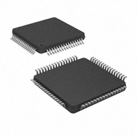
LQFP80
14 x 14
LQFP64
14 x 14
LQFP64
10 x 10
5 timers
■
Main clock controller with Real-time base,
Beep and Clock-out capabilities
■ Configurable watchdog timer
■ Two 16-bit timers with 2 input captures, 2
output compares, external clock input on 1
timer, PWM and pulse generator modes
■ 8-bit PWM auto-reload timer with 2 input
captures, 4 PWM outputs, output compare and
time base interrupt, external clock with event
detector
4 communications interfaces
■
SPI synchronous serial interface
■ SCI asynchronous serial interface
2
■ I C multimaster interface (SMbus V1.1
compliant)
■ CAN interface (2.0B passive)
Instruction set
■
8-bit data manipulation
■ 63 basic instructions
■ 17 main addressing modes
■ 8x8 unsigned multiply instruction
Development tools
■
Full HW/SW development pkg, ICT capability
Table 1.
Device summary
Reference
Part number
ST72521R6-Auto
ST72521R9-Auto
ST72521xx-Auto
ST72521AR9-Auto
ST72521M9-Auto
July 2010
Doc ID 17660 Rev 1
1/276
www.st.com
1
�Contents
ST72521xx-Auto
Contents
1
Description . . . . . . . . . . . . . . . . . . . . . . . . . . . . . . . . . . . . . . . . . . . . . . . . 19
2
Package pinout and pin description . . . . . . . . . . . . . . . . . . . . . . . . . . . 21
2.1
Package pinout . . . . . . . . . . . . . . . . . . . . . . . . . . . . . . . . . . . . . . . . . . . . . 21
2.2
Pin description . . . . . . . . . . . . . . . . . . . . . . . . . . . . . . . . . . . . . . . . . . . . . 23
3
Register and memory map . . . . . . . . . . . . . . . . . . . . . . . . . . . . . . . . . . . 28
4
Flash program memory . . . . . . . . . . . . . . . . . . . . . . . . . . . . . . . . . . . . . 32
4.1
Introduction . . . . . . . . . . . . . . . . . . . . . . . . . . . . . . . . . . . . . . . . . . . . . . . 32
4.2
Main features . . . . . . . . . . . . . . . . . . . . . . . . . . . . . . . . . . . . . . . . . . . . . . 32
4.3
Structure . . . . . . . . . . . . . . . . . . . . . . . . . . . . . . . . . . . . . . . . . . . . . . . . . . 32
4.3.1
5
6
2/276
Readout protection . . . . . . . . . . . . . . . . . . . . . . . . . . . . . . . . . . . . . . . . 33
4.4
ICC interface . . . . . . . . . . . . . . . . . . . . . . . . . . . . . . . . . . . . . . . . . . . . . . 33
4.5
ICP (in-circuit programming) . . . . . . . . . . . . . . . . . . . . . . . . . . . . . . . . . . 34
4.6
IAP (in-application programming) . . . . . . . . . . . . . . . . . . . . . . . . . . . . . . . 35
4.7
Related documentation . . . . . . . . . . . . . . . . . . . . . . . . . . . . . . . . . . . . . . 35
4.8
Flash control/status register (FCSR) . . . . . . . . . . . . . . . . . . . . . . . . . . . . 35
Central processing unit (CPU) . . . . . . . . . . . . . . . . . . . . . . . . . . . . . . . . 36
5.1
Introduction . . . . . . . . . . . . . . . . . . . . . . . . . . . . . . . . . . . . . . . . . . . . . . . 36
5.2
Main features . . . . . . . . . . . . . . . . . . . . . . . . . . . . . . . . . . . . . . . . . . . . . . 36
5.3
CPU registers . . . . . . . . . . . . . . . . . . . . . . . . . . . . . . . . . . . . . . . . . . . . . . 36
5.3.1
Accumulator (A) . . . . . . . . . . . . . . . . . . . . . . . . . . . . . . . . . . . . . . . . . . . 37
5.3.2
Index registers (X and Y) . . . . . . . . . . . . . . . . . . . . . . . . . . . . . . . . . . . . 37
5.3.3
Program counter (PC) . . . . . . . . . . . . . . . . . . . . . . . . . . . . . . . . . . . . . . 37
5.3.4
Condition code (CC) register . . . . . . . . . . . . . . . . . . . . . . . . . . . . . . . . . 37
5.3.5
Stack pointer (SP) register . . . . . . . . . . . . . . . . . . . . . . . . . . . . . . . . . . . 38
Supply, reset and clock management . . . . . . . . . . . . . . . . . . . . . . . . . . 40
6.1
Introduction . . . . . . . . . . . . . . . . . . . . . . . . . . . . . . . . . . . . . . . . . . . . . . . 40
6.2
Main features . . . . . . . . . . . . . . . . . . . . . . . . . . . . . . . . . . . . . . . . . . . . . . 40
6.3
Phase locked loop . . . . . . . . . . . . . . . . . . . . . . . . . . . . . . . . . . . . . . . . . . 41
Doc ID 17660 Rev 1
�ST72521xx-Auto
6.4
Multi-oscillator (MO) . . . . . . . . . . . . . . . . . . . . . . . . . . . . . . . . . . . . . . . . . 41
6.5
Reset sequence manager (RSM) . . . . . . . . . . . . . . . . . . . . . . . . . . . . . . . 43
6.6
7
9
6.5.1
Introduction . . . . . . . . . . . . . . . . . . . . . . . . . . . . . . . . . . . . . . . . . . . . . . 43
6.5.2
Asynchronous external RESET pin . . . . . . . . . . . . . . . . . . . . . . . . . . . . 44
6.5.3
External power-on RESET . . . . . . . . . . . . . . . . . . . . . . . . . . . . . . . . . . . 44
6.5.4
Internal low voltage detector (LVD) RESET . . . . . . . . . . . . . . . . . . . . . . 44
6.5.5
Internal watchdog RESET . . . . . . . . . . . . . . . . . . . . . . . . . . . . . . . . . . . 45
System integrity management (SI) . . . . . . . . . . . . . . . . . . . . . . . . . . . . . . 46
6.6.1
Low voltage detector (LVD) . . . . . . . . . . . . . . . . . . . . . . . . . . . . . . . . . . 46
6.6.2
Auxiliary voltage detector (AVD) . . . . . . . . . . . . . . . . . . . . . . . . . . . . . . 47
6.6.3
Low power modes . . . . . . . . . . . . . . . . . . . . . . . . . . . . . . . . . . . . . . . . . 49
6.6.4
Interrupts . . . . . . . . . . . . . . . . . . . . . . . . . . . . . . . . . . . . . . . . . . . . . . . . 49
6.6.5
System Integrity (SI) Control/Status register (SICSR) . . . . . . . . . . . . . . 50
Interrupts . . . . . . . . . . . . . . . . . . . . . . . . . . . . . . . . . . . . . . . . . . . . . . . . . 52
7.1
Introduction . . . . . . . . . . . . . . . . . . . . . . . . . . . . . . . . . . . . . . . . . . . . . . . 52
7.2
Masking and processing flow . . . . . . . . . . . . . . . . . . . . . . . . . . . . . . . . . . 52
7.3
Interrupts and low power modes . . . . . . . . . . . . . . . . . . . . . . . . . . . . . . . 55
7.4
Concurrent and nested management . . . . . . . . . . . . . . . . . . . . . . . . . . . . 55
7.5
Interrupt register description . . . . . . . . . . . . . . . . . . . . . . . . . . . . . . . . . . 56
7.6
8
Contents
7.5.1
CPU CC register interrupt bits . . . . . . . . . . . . . . . . . . . . . . . . . . . . . . . . 56
7.5.2
Interrupt software priority registers (ISPRx) . . . . . . . . . . . . . . . . . . . . . . 57
External interrupts . . . . . . . . . . . . . . . . . . . . . . . . . . . . . . . . . . . . . . . . . . 60
7.6.1
I/O port interrupt sensitivity . . . . . . . . . . . . . . . . . . . . . . . . . . . . . . . . . . 60
7.6.2
External interrupt control register (EICR) . . . . . . . . . . . . . . . . . . . . . . . . 62
Power saving modes . . . . . . . . . . . . . . . . . . . . . . . . . . . . . . . . . . . . . . . . 65
8.1
Introduction . . . . . . . . . . . . . . . . . . . . . . . . . . . . . . . . . . . . . . . . . . . . . . . 65
8.2
Slow mode . . . . . . . . . . . . . . . . . . . . . . . . . . . . . . . . . . . . . . . . . . . . . . . . 65
8.3
Wait mode . . . . . . . . . . . . . . . . . . . . . . . . . . . . . . . . . . . . . . . . . . . . . . . . 66
8.4
Active Halt and Halt modes . . . . . . . . . . . . . . . . . . . . . . . . . . . . . . . . . . . 68
8.4.1
Active Halt mode . . . . . . . . . . . . . . . . . . . . . . . . . . . . . . . . . . . . . . . . . . 68
8.4.2
Halt mode . . . . . . . . . . . . . . . . . . . . . . . . . . . . . . . . . . . . . . . . . . . . . . . 70
I/O ports . . . . . . . . . . . . . . . . . . . . . . . . . . . . . . . . . . . . . . . . . . . . . . . . . . 73
9.1
Introduction . . . . . . . . . . . . . . . . . . . . . . . . . . . . . . . . . . . . . . . . . . . . . . . 73
Doc ID 17660 Rev 1
3/276
�Contents
ST72521xx-Auto
9.2
10
Functional description . . . . . . . . . . . . . . . . . . . . . . . . . . . . . . . . . . . . . . . 73
9.2.1
Input modes . . . . . . . . . . . . . . . . . . . . . . . . . . . . . . . . . . . . . . . . . . . . . . 73
9.2.2
Output modes . . . . . . . . . . . . . . . . . . . . . . . . . . . . . . . . . . . . . . . . . . . . 74
9.2.3
Alternate functions . . . . . . . . . . . . . . . . . . . . . . . . . . . . . . . . . . . . . . . . . 74
9.3
I/O port implementation . . . . . . . . . . . . . . . . . . . . . . . . . . . . . . . . . . . . . . 77
9.4
Low power modes . . . . . . . . . . . . . . . . . . . . . . . . . . . . . . . . . . . . . . . . . . 78
9.5
Interrupts . . . . . . . . . . . . . . . . . . . . . . . . . . . . . . . . . . . . . . . . . . . . . . . . . 78
Watchdog timer (WDG) . . . . . . . . . . . . . . . . . . . . . . . . . . . . . . . . . . . . . . 80
10.1
Introduction . . . . . . . . . . . . . . . . . . . . . . . . . . . . . . . . . . . . . . . . . . . . . . . 80
10.2
Main features . . . . . . . . . . . . . . . . . . . . . . . . . . . . . . . . . . . . . . . . . . . . . . 80
10.3
Functional description . . . . . . . . . . . . . . . . . . . . . . . . . . . . . . . . . . . . . . . 80
10.4
How to program the watchdog timeout . . . . . . . . . . . . . . . . . . . . . . . . . . . 81
10.5
Low power modes . . . . . . . . . . . . . . . . . . . . . . . . . . . . . . . . . . . . . . . . . . 83
10.6
Hardware watchdog option . . . . . . . . . . . . . . . . . . . . . . . . . . . . . . . . . . . . 83
10.7
Using Halt mode with the WDG (WDGHALT option) . . . . . . . . . . . . . . . . 83
10.8
Interrupts . . . . . . . . . . . . . . . . . . . . . . . . . . . . . . . . . . . . . . . . . . . . . . . . . 83
10.9
Register description . . . . . . . . . . . . . . . . . . . . . . . . . . . . . . . . . . . . . . . . . 84
10.9.1
11
12
4/276
Control register (WDGCR) . . . . . . . . . . . . . . . . . . . . . . . . . . . . . . . . . . . 84
Main clock controller with real-time clock and beeper (MCC/RTC) . . 85
11.1
Introduction . . . . . . . . . . . . . . . . . . . . . . . . . . . . . . . . . . . . . . . . . . . . . . . 85
11.2
Programmable CPU clock prescaler . . . . . . . . . . . . . . . . . . . . . . . . . . . . 85
11.3
Clock-out capability . . . . . . . . . . . . . . . . . . . . . . . . . . . . . . . . . . . . . . . . . 85
11.4
Real-time clock timer (RTC) . . . . . . . . . . . . . . . . . . . . . . . . . . . . . . . . . . . 85
11.5
Beeper . . . . . . . . . . . . . . . . . . . . . . . . . . . . . . . . . . . . . . . . . . . . . . . . . . . 85
11.6
Low power modes . . . . . . . . . . . . . . . . . . . . . . . . . . . . . . . . . . . . . . . . . . 86
11.7
Interrupts . . . . . . . . . . . . . . . . . . . . . . . . . . . . . . . . . . . . . . . . . . . . . . . . . 86
11.8
Main clock controller registers . . . . . . . . . . . . . . . . . . . . . . . . . . . . . . . . . 87
11.8.1
MCC control/status register (MCCSR) . . . . . . . . . . . . . . . . . . . . . . . . . . 87
11.8.2
MCC beep control register (MCCBCR) . . . . . . . . . . . . . . . . . . . . . . . . . 88
PWM auto-reload timer (ART) . . . . . . . . . . . . . . . . . . . . . . . . . . . . . . . . 90
12.1
Introduction . . . . . . . . . . . . . . . . . . . . . . . . . . . . . . . . . . . . . . . . . . . . . . . 90
12.2
Functional description . . . . . . . . . . . . . . . . . . . . . . . . . . . . . . . . . . . . . . . 91
Doc ID 17660 Rev 1
�ST72521xx-Auto
12.3
13
Contents
12.2.1
Counter . . . . . . . . . . . . . . . . . . . . . . . . . . . . . . . . . . . . . . . . . . . . . . . . . 91
12.2.2
Counter clock and prescaler . . . . . . . . . . . . . . . . . . . . . . . . . . . . . . . . . 91
12.2.3
Counter and prescaler initialization . . . . . . . . . . . . . . . . . . . . . . . . . . . . 91
12.2.4
Output compare control . . . . . . . . . . . . . . . . . . . . . . . . . . . . . . . . . . . . . 91
12.2.5
Independent PWM signal generation . . . . . . . . . . . . . . . . . . . . . . . . . . . 92
12.2.6
Output compare and time base interrupt . . . . . . . . . . . . . . . . . . . . . . . . 93
12.2.7
External clock and event detector mode . . . . . . . . . . . . . . . . . . . . . . . . 93
12.2.8
Input capture function . . . . . . . . . . . . . . . . . . . . . . . . . . . . . . . . . . . . . . 94
12.2.9
External interrupt capability . . . . . . . . . . . . . . . . . . . . . . . . . . . . . . . . . . 95
ART registers . . . . . . . . . . . . . . . . . . . . . . . . . . . . . . . . . . . . . . . . . . . . . . 96
12.3.1
Control/status register (ARTCSR) . . . . . . . . . . . . . . . . . . . . . . . . . . . . . 96
12.3.2
Counter access register (ARTCAR) . . . . . . . . . . . . . . . . . . . . . . . . . . . . 97
12.3.3
Auto-reload register (ARTARR) . . . . . . . . . . . . . . . . . . . . . . . . . . . . . . . 97
12.3.4
PWM control register (PWMCR) . . . . . . . . . . . . . . . . . . . . . . . . . . . . . . 98
12.3.5
Duty cycle registers (PWMDCRx) . . . . . . . . . . . . . . . . . . . . . . . . . . . . . 99
12.3.6
Input capture control / status register (ARTICCSR) . . . . . . . . . . . . . . . . 99
12.3.7
Input capture registers (ARTICRx) . . . . . . . . . . . . . . . . . . . . . . . . . . . . 100
16-bit timer . . . . . . . . . . . . . . . . . . . . . . . . . . . . . . . . . . . . . . . . . . . . . . . 101
13.1
Introduction . . . . . . . . . . . . . . . . . . . . . . . . . . . . . . . . . . . . . . . . . . . . . . 101
13.2
Main features . . . . . . . . . . . . . . . . . . . . . . . . . . . . . . . . . . . . . . . . . . . . . 101
13.3
Functional description . . . . . . . . . . . . . . . . . . . . . . . . . . . . . . . . . . . . . . 102
13.3.1
Counter . . . . . . . . . . . . . . . . . . . . . . . . . . . . . . . . . . . . . . . . . . . . . . . . 102
13.3.2
External clock . . . . . . . . . . . . . . . . . . . . . . . . . . . . . . . . . . . . . . . . . . . 105
13.3.3
Input capture . . . . . . . . . . . . . . . . . . . . . . . . . . . . . . . . . . . . . . . . . . . . 106
13.3.4
Output compare . . . . . . . . . . . . . . . . . . . . . . . . . . . . . . . . . . . . . . . . . . 108
13.3.5
Forced compare output capability . . . . . . . . . . . . . . . . . . . . . . . . . . . . 109
13.3.6
One Pulse mode . . . . . . . . . . . . . . . . . . . . . . . . . . . . . . . . . . . . . . . . . 111
13.3.7
Pulse width modulation mode . . . . . . . . . . . . . . . . . . . . . . . . . . . . . . . 113
13.4
Low power modes . . . . . . . . . . . . . . . . . . . . . . . . . . . . . . . . . . . . . . . . . 115
13.5
Interrupts . . . . . . . . . . . . . . . . . . . . . . . . . . . . . . . . . . . . . . . . . . . . . . . . 115
13.6
Summary of timer modes . . . . . . . . . . . . . . . . . . . . . . . . . . . . . . . . . . . . 115
13.7
16-bit timer registers . . . . . . . . . . . . . . . . . . . . . . . . . . . . . . . . . . . . . . . . 116
13.7.1
Control register 1 (CR1) . . . . . . . . . . . . . . . . . . . . . . . . . . . . . . . . . . . . 116
13.7.2
Control register 2 (CR2) . . . . . . . . . . . . . . . . . . . . . . . . . . . . . . . . . . . . 117
13.7.3
Control/status register (CSR) . . . . . . . . . . . . . . . . . . . . . . . . . . . . . . . . 118
Doc ID 17660 Rev 1
5/276
�Contents
ST72521xx-Auto
13.7.4
Input capture 1 high register (IC1HR) . . . . . . . . . . . . . . . . . . . . . . . . . 119
13.7.5
Input capture 1 low register (IC1LR) . . . . . . . . . . . . . . . . . . . . . . . . . . 120
13.7.6
Output compare 1 high register (OC1HR) . . . . . . . . . . . . . . . . . . . . . . 120
13.7.7
Output compare 1 low register (OC1LR) . . . . . . . . . . . . . . . . . . . . . . . 120
13.7.8
Output compare 2 high register (OC2HR) . . . . . . . . . . . . . . . . . . . . . . 120
13.7.9
Output compare 2 low register (OC2LR) . . . . . . . . . . . . . . . . . . . . . . . 121
13.7.10 Counter high register (CHR) . . . . . . . . . . . . . . . . . . . . . . . . . . . . . . . . 121
13.7.11 Counter low register (CLR) . . . . . . . . . . . . . . . . . . . . . . . . . . . . . . . . . 121
13.7.12 Alternate counter high register (ACHR) . . . . . . . . . . . . . . . . . . . . . . . . 121
13.7.13 Alternate counter low register (ACLR) . . . . . . . . . . . . . . . . . . . . . . . . . 122
13.7.14 Input capture 2 high register (IC2HR) . . . . . . . . . . . . . . . . . . . . . . . . . 122
13.7.15 Input capture 2 low register (IC2LR) . . . . . . . . . . . . . . . . . . . . . . . . . . 122
14
Serial peripheral interface (SPI) . . . . . . . . . . . . . . . . . . . . . . . . . . . . . . 124
14.1
Introduction . . . . . . . . . . . . . . . . . . . . . . . . . . . . . . . . . . . . . . . . . . . . . . 124
14.2
Main features . . . . . . . . . . . . . . . . . . . . . . . . . . . . . . . . . . . . . . . . . . . . . 124
14.3
General description . . . . . . . . . . . . . . . . . . . . . . . . . . . . . . . . . . . . . . . . 124
14.3.1
Functional description . . . . . . . . . . . . . . . . . . . . . . . . . . . . . . . . . . . . . 125
14.3.2
Slave select management . . . . . . . . . . . . . . . . . . . . . . . . . . . . . . . . . . 126
14.3.3
Master mode operation . . . . . . . . . . . . . . . . . . . . . . . . . . . . . . . . . . . . 127
14.3.4
Master mode transmit sequence . . . . . . . . . . . . . . . . . . . . . . . . . . . . . 128
14.3.5
Slave mode operation . . . . . . . . . . . . . . . . . . . . . . . . . . . . . . . . . . . . . 128
14.3.6
Slave mode transmit sequence . . . . . . . . . . . . . . . . . . . . . . . . . . . . . . 128
14.4
Clock phase and clock polarity . . . . . . . . . . . . . . . . . . . . . . . . . . . . . . . . 129
14.5
Error flags . . . . . . . . . . . . . . . . . . . . . . . . . . . . . . . . . . . . . . . . . . . . . . . . 131
14.6
14.5.1
Master mode fault (MODF) . . . . . . . . . . . . . . . . . . . . . . . . . . . . . . . . . 131
14.5.2
Overrun condition (OVR) . . . . . . . . . . . . . . . . . . . . . . . . . . . . . . . . . . . 131
14.5.3
Write collision error (WCOL) . . . . . . . . . . . . . . . . . . . . . . . . . . . . . . . . 131
14.5.4
Single master systems . . . . . . . . . . . . . . . . . . . . . . . . . . . . . . . . . . . . . 132
Low power modes . . . . . . . . . . . . . . . . . . . . . . . . . . . . . . . . . . . . . . . . . 133
14.6.1
6/276
Using the SPI to wake up the MCU from Halt mode . . . . . . . . . . . . . . 133
14.7
Interrupts . . . . . . . . . . . . . . . . . . . . . . . . . . . . . . . . . . . . . . . . . . . . . . . . 133
14.8
SPI registers . . . . . . . . . . . . . . . . . . . . . . . . . . . . . . . . . . . . . . . . . . . . . . 134
14.8.1
Control register (SPICR) . . . . . . . . . . . . . . . . . . . . . . . . . . . . . . . . . . . 134
14.8.2
Control/status register (SPICSR) . . . . . . . . . . . . . . . . . . . . . . . . . . . . . 135
14.8.3
Data I/O register (SPIDR) . . . . . . . . . . . . . . . . . . . . . . . . . . . . . . . . . . 136
Doc ID 17660 Rev 1
�ST72521xx-Auto
15
16
Contents
Serial communications interface (SCI) . . . . . . . . . . . . . . . . . . . . . . . . 138
15.1
Introduction . . . . . . . . . . . . . . . . . . . . . . . . . . . . . . . . . . . . . . . . . . . . . . 138
15.2
Main features . . . . . . . . . . . . . . . . . . . . . . . . . . . . . . . . . . . . . . . . . . . . . 138
15.3
General description . . . . . . . . . . . . . . . . . . . . . . . . . . . . . . . . . . . . . . . . 139
15.4
Functional description . . . . . . . . . . . . . . . . . . . . . . . . . . . . . . . . . . . . . . 141
15.4.1
Serial data format . . . . . . . . . . . . . . . . . . . . . . . . . . . . . . . . . . . . . . . . 141
15.4.2
Transmitter . . . . . . . . . . . . . . . . . . . . . . . . . . . . . . . . . . . . . . . . . . . . . . 142
15.4.3
Receiver . . . . . . . . . . . . . . . . . . . . . . . . . . . . . . . . . . . . . . . . . . . . . . . . 143
15.5
Low power modes . . . . . . . . . . . . . . . . . . . . . . . . . . . . . . . . . . . . . . . . . 149
15.6
Interrupts . . . . . . . . . . . . . . . . . . . . . . . . . . . . . . . . . . . . . . . . . . . . . . . . 149
15.7
SCI registers . . . . . . . . . . . . . . . . . . . . . . . . . . . . . . . . . . . . . . . . . . . . . . 150
15.7.1
Status register (SCISR) . . . . . . . . . . . . . . . . . . . . . . . . . . . . . . . . . . . . 150
15.7.2
Control register 1 (SCICR1) . . . . . . . . . . . . . . . . . . . . . . . . . . . . . . . . . 152
15.7.3
Control register 2 (SCICR2) . . . . . . . . . . . . . . . . . . . . . . . . . . . . . . . . . 153
15.7.4
Data register (SCIDR) . . . . . . . . . . . . . . . . . . . . . . . . . . . . . . . . . . . . . 154
15.7.5
Baud rate register (SCIBRR) . . . . . . . . . . . . . . . . . . . . . . . . . . . . . . . . 154
15.7.6
Extended receive prescaler division register (SCIERPR) . . . . . . . . . . 155
15.7.7
Extended transmit prescaler division register (SCIETPR) . . . . . . . . . . 156
I2C bus interface (I2C) . . . . . . . . . . . . . . . . . . . . . . . . . . . . . . . . . . . . . 158
16.1
Introduction . . . . . . . . . . . . . . . . . . . . . . . . . . . . . . . . . . . . . . . . . . . . . . 158
16.2
Main features . . . . . . . . . . . . . . . . . . . . . . . . . . . . . . . . . . . . . . . . . . . . . 158
16.3
16.4
16.2.1
I2C master features . . . . . . . . . . . . . . . . . . . . . . . . . . . . . . . . . . . . . . . 158
16.2.2
I2C slave features . . . . . . . . . . . . . . . . . . . . . . . . . . . . . . . . . . . . . . . . 158
General description . . . . . . . . . . . . . . . . . . . . . . . . . . . . . . . . . . . . . . . . 159
16.3.1
Mode selection . . . . . . . . . . . . . . . . . . . . . . . . . . . . . . . . . . . . . . . . . . . 159
16.3.2
Communication flow . . . . . . . . . . . . . . . . . . . . . . . . . . . . . . . . . . . . . . . 159
16.3.3
SDA/SCL line control . . . . . . . . . . . . . . . . . . . . . . . . . . . . . . . . . . . . . . 160
Functional description . . . . . . . . . . . . . . . . . . . . . . . . . . . . . . . . . . . . . . 161
16.4.1
Slave mode . . . . . . . . . . . . . . . . . . . . . . . . . . . . . . . . . . . . . . . . . . . . . 161
16.4.2
Master mode . . . . . . . . . . . . . . . . . . . . . . . . . . . . . . . . . . . . . . . . . . . . 162
16.5
Low power modes . . . . . . . . . . . . . . . . . . . . . . . . . . . . . . . . . . . . . . . . . 166
16.6
Interrupts . . . . . . . . . . . . . . . . . . . . . . . . . . . . . . . . . . . . . . . . . . . . . . . . 166
16.7
Register description . . . . . . . . . . . . . . . . . . . . . . . . . . . . . . . . . . . . . . . . 167
16.7.1
I2C control register (CR) . . . . . . . . . . . . . . . . . . . . . . . . . . . . . . . . . . . 167
Doc ID 17660 Rev 1
7/276
�Contents
17
ST72521xx-Auto
I2C status register 1 (SR1) . . . . . . . . . . . . . . . . . . . . . . . . . . . . . . . . . 168
16.7.3
I2C status register 2 (SR2) . . . . . . . . . . . . . . . . . . . . . . . . . . . . . . . . . 170
16.7.4
I2C clock control register (CCR) . . . . . . . . . . . . . . . . . . . . . . . . . . . . . 171
16.7.5
I2C data register (DR) . . . . . . . . . . . . . . . . . . . . . . . . . . . . . . . . . . . . . 172
16.7.6
I2C own address register (OAR1) . . . . . . . . . . . . . . . . . . . . . . . . . . . . 172
16.7.7
I2C own address register (OAR2) . . . . . . . . . . . . . . . . . . . . . . . . . . . . 173
Controller area network (CAN) . . . . . . . . . . . . . . . . . . . . . . . . . . . . . . . 175
17.1
Introduction . . . . . . . . . . . . . . . . . . . . . . . . . . . . . . . . . . . . . . . . . . . . . . 175
17.2
Main features . . . . . . . . . . . . . . . . . . . . . . . . . . . . . . . . . . . . . . . . . . . . . 176
17.3
Functional description . . . . . . . . . . . . . . . . . . . . . . . . . . . . . . . . . . . . . . 176
17.4
17.5
18
16.7.2
17.3.1
Frame formats . . . . . . . . . . . . . . . . . . . . . . . . . . . . . . . . . . . . . . . . . . . 176
17.3.2
Hardware blocks . . . . . . . . . . . . . . . . . . . . . . . . . . . . . . . . . . . . . . . . . 177
17.3.3
Modes of operation . . . . . . . . . . . . . . . . . . . . . . . . . . . . . . . . . . . . . . . 179
17.3.4
Bit timing logic . . . . . . . . . . . . . . . . . . . . . . . . . . . . . . . . . . . . . . . . . . . 181
Register description . . . . . . . . . . . . . . . . . . . . . . . . . . . . . . . . . . . . . . . . 182
17.4.1
General purpose registers . . . . . . . . . . . . . . . . . . . . . . . . . . . . . . . . . . 182
17.4.2
Paged registers . . . . . . . . . . . . . . . . . . . . . . . . . . . . . . . . . . . . . . . . . . 187
List of CAN cell limitations . . . . . . . . . . . . . . . . . . . . . . . . . . . . . . . . . . . 196
17.5.1
Omitted SOF bit . . . . . . . . . . . . . . . . . . . . . . . . . . . . . . . . . . . . . . . . . . 196
17.5.2
CPU write access (more than one cycle) corrupts CAN frame . . . . . . 196
17.5.3
Unexpected message transmission . . . . . . . . . . . . . . . . . . . . . . . . . . . 197
17.5.4
WKPS functionality . . . . . . . . . . . . . . . . . . . . . . . . . . . . . . . . . . . . . . . 202
17.5.5
Bus-off state not entered . . . . . . . . . . . . . . . . . . . . . . . . . . . . . . . . . . . 203
10-bit A/D converter (ADC) . . . . . . . . . . . . . . . . . . . . . . . . . . . . . . . . . . 205
18.1
Introduction . . . . . . . . . . . . . . . . . . . . . . . . . . . . . . . . . . . . . . . . . . . . . . 205
18.2
Main features . . . . . . . . . . . . . . . . . . . . . . . . . . . . . . . . . . . . . . . . . . . . . 205
18.3
Functional description . . . . . . . . . . . . . . . . . . . . . . . . . . . . . . . . . . . . . . 206
18.3.1
A/D converter configuration . . . . . . . . . . . . . . . . . . . . . . . . . . . . . . . . . 206
18.3.2
Starting the conversion . . . . . . . . . . . . . . . . . . . . . . . . . . . . . . . . . . . . 206
18.3.3
Changing the conversion channel . . . . . . . . . . . . . . . . . . . . . . . . . . . . 207
18.4
Low power modes . . . . . . . . . . . . . . . . . . . . . . . . . . . . . . . . . . . . . . . . . 207
18.5
Interrupts . . . . . . . . . . . . . . . . . . . . . . . . . . . . . . . . . . . . . . . . . . . . . . . . 207
18.6
ADC registers . . . . . . . . . . . . . . . . . . . . . . . . . . . . . . . . . . . . . . . . . . . . . 207
18.6.1
8/276
Control/status register (ADCCSR) . . . . . . . . . . . . . . . . . . . . . . . . . . . . 207
Doc ID 17660 Rev 1
�ST72521xx-Auto
19
Contents
18.6.2
Data register (ADCDRH) . . . . . . . . . . . . . . . . . . . . . . . . . . . . . . . . . . . 208
18.6.3
Data register (ADCDRL) . . . . . . . . . . . . . . . . . . . . . . . . . . . . . . . . . . . 209
18.6.4
ADC register map and reset values . . . . . . . . . . . . . . . . . . . . . . . . . . . 209
Instruction set . . . . . . . . . . . . . . . . . . . . . . . . . . . . . . . . . . . . . . . . . . . . 210
19.1
19.2
CPU addressing modes . . . . . . . . . . . . . . . . . . . . . . . . . . . . . . . . . . . . . 210
19.1.1
Inherent . . . . . . . . . . . . . . . . . . . . . . . . . . . . . . . . . . . . . . . . . . . . . . . . 211
19.1.2
Immediate . . . . . . . . . . . . . . . . . . . . . . . . . . . . . . . . . . . . . . . . . . . . . . 212
19.1.3
Direct . . . . . . . . . . . . . . . . . . . . . . . . . . . . . . . . . . . . . . . . . . . . . . . . . . 212
19.1.4
Indexed (no offset, short, long) . . . . . . . . . . . . . . . . . . . . . . . . . . . . . . 212
19.1.5
Indirect (short, long) . . . . . . . . . . . . . . . . . . . . . . . . . . . . . . . . . . . . . . . 213
19.1.6
Indirect Indexed (Short, Long) . . . . . . . . . . . . . . . . . . . . . . . . . . . . . . . 213
19.1.7
Relative (Direct, Indirect) . . . . . . . . . . . . . . . . . . . . . . . . . . . . . . . . . . . 214
Instruction groups . . . . . . . . . . . . . . . . . . . . . . . . . . . . . . . . . . . . . . . . . . 214
19.2.1
20
Using a prebyte . . . . . . . . . . . . . . . . . . . . . . . . . . . . . . . . . . . . . . . . . . 215
Electrical characteristics . . . . . . . . . . . . . . . . . . . . . . . . . . . . . . . . . . . 218
20.1
20.2
20.3
20.4
Parameter conditions . . . . . . . . . . . . . . . . . . . . . . . . . . . . . . . . . . . . . . . 218
20.1.1
Minimum and maximum values . . . . . . . . . . . . . . . . . . . . . . . . . . . . . . 218
20.1.2
Typical values . . . . . . . . . . . . . . . . . . . . . . . . . . . . . . . . . . . . . . . . . . . . 218
20.1.3
Typical curves . . . . . . . . . . . . . . . . . . . . . . . . . . . . . . . . . . . . . . . . . . . 218
20.1.4
Loading capacitor . . . . . . . . . . . . . . . . . . . . . . . . . . . . . . . . . . . . . . . . 218
20.1.5
Pin input voltage . . . . . . . . . . . . . . . . . . . . . . . . . . . . . . . . . . . . . . . . . 218
Absolute maximum ratings . . . . . . . . . . . . . . . . . . . . . . . . . . . . . . . . . . . 219
20.2.1
Voltage characteristics . . . . . . . . . . . . . . . . . . . . . . . . . . . . . . . . . . . . . 219
20.2.2
Current characteristics . . . . . . . . . . . . . . . . . . . . . . . . . . . . . . . . . . . . . 220
20.2.3
Thermal characteristics . . . . . . . . . . . . . . . . . . . . . . . . . . . . . . . . . . . . 220
Operating conditions . . . . . . . . . . . . . . . . . . . . . . . . . . . . . . . . . . . . . . . 221
20.3.1
General operating conditions . . . . . . . . . . . . . . . . . . . . . . . . . . . . . . . . 221
20.3.2
Operating conditions with low voltage detector (LVD) . . . . . . . . . . . . . 222
20.3.3
Auxiliary voltage detector (AVD) thresholds . . . . . . . . . . . . . . . . . . . . . 222
20.3.4
External voltage detector (EVD) thresholds . . . . . . . . . . . . . . . . . . . . . 223
Supply current characteristics . . . . . . . . . . . . . . . . . . . . . . . . . . . . . . . . 224
20.4.1
Current consumption . . . . . . . . . . . . . . . . . . . . . . . . . . . . . . . . . . . . . . 224
20.4.2
Supply and clock managers . . . . . . . . . . . . . . . . . . . . . . . . . . . . . . . . . 226
20.4.3
On-chip peripherals . . . . . . . . . . . . . . . . . . . . . . . . . . . . . . . . . . . . . . . 227
Doc ID 17660 Rev 1
9/276
�Contents
ST72521xx-Auto
20.5
20.6
20.7
20.8
20.9
Clock and timing characteristics . . . . . . . . . . . . . . . . . . . . . . . . . . . . . . . 228
20.5.1
General timings . . . . . . . . . . . . . . . . . . . . . . . . . . . . . . . . . . . . . . . . . . 228
20.5.2
External clock source . . . . . . . . . . . . . . . . . . . . . . . . . . . . . . . . . . . . . . 228
20.5.3
Crystal and ceramic resonator oscillators . . . . . . . . . . . . . . . . . . . . . . 229
20.5.4
RC oscillators . . . . . . . . . . . . . . . . . . . . . . . . . . . . . . . . . . . . . . . . . . . . 230
20.5.5
PLL characteristics . . . . . . . . . . . . . . . . . . . . . . . . . . . . . . . . . . . . . . . 231
Memory characteristics . . . . . . . . . . . . . . . . . . . . . . . . . . . . . . . . . . . . . 232
20.6.1
RAM and hardware registers . . . . . . . . . . . . . . . . . . . . . . . . . . . . . . . . 232
20.6.2
Flash memory . . . . . . . . . . . . . . . . . . . . . . . . . . . . . . . . . . . . . . . . . . . 232
EMC (electromagnetic compatibility) characteristics . . . . . . . . . . . . . . . 233
20.7.1
Functional EMS (electromagnetic susceptibility) . . . . . . . . . . . . . . . . . 233
20.7.2
EMI (electromagnetic interference) . . . . . . . . . . . . . . . . . . . . . . . . . . . 234
20.7.3
Absolute maximum ratings (electrical sensitivity) . . . . . . . . . . . . . . . . 235
I/O port pin characteristics . . . . . . . . . . . . . . . . . . . . . . . . . . . . . . . . . . . 236
20.8.1
General characteristics . . . . . . . . . . . . . . . . . . . . . . . . . . . . . . . . . . . . 236
20.8.2
Output driving current . . . . . . . . . . . . . . . . . . . . . . . . . . . . . . . . . . . . . 237
Control pin characteristics . . . . . . . . . . . . . . . . . . . . . . . . . . . . . . . . . . . 240
20.9.1
Asynchronous RESET pin . . . . . . . . . . . . . . . . . . . . . . . . . . . . . . . . . . 240
20.9.2
ICCSEL/VPP pin . . . . . . . . . . . . . . . . . . . . . . . . . . . . . . . . . . . . . . . . . . 242
20.10 Timer peripheral characteristics . . . . . . . . . . . . . . . . . . . . . . . . . . . . . . . 243
20.11 Communication interface characteristics . . . . . . . . . . . . . . . . . . . . . . . . 244
20.11.1 SPI (serial peripheral interface) . . . . . . . . . . . . . . . . . . . . . . . . . . . . . . 244
20.11.2 I2C - inter IC control interface . . . . . . . . . . . . . . . . . . . . . . . . . . . . . . . 247
20.11.3 CAN - Controller area network interface . . . . . . . . . . . . . . . . . . . . . . . 249
20.12 10-bit ADC characteristics . . . . . . . . . . . . . . . . . . . . . . . . . . . . . . . . . . . 249
20.12.1 Analog power supply and reference pins . . . . . . . . . . . . . . . . . . . . . . . 250
20.12.2 General PCB design guidelines . . . . . . . . . . . . . . . . . . . . . . . . . . . . . . 251
20.12.3 ADC accuracy . . . . . . . . . . . . . . . . . . . . . . . . . . . . . . . . . . . . . . . . . . . 252
21
22
Package characteristics . . . . . . . . . . . . . . . . . . . . . . . . . . . . . . . . . . . . 253
21.1
Thermal characteristics . . . . . . . . . . . . . . . . . . . . . . . . . . . . . . . . . . . . . 256
21.2
Ecopack information . . . . . . . . . . . . . . . . . . . . . . . . . . . . . . . . . . . . . . . . 256
21.3
Packaging for automatic handling . . . . . . . . . . . . . . . . . . . . . . . . . . . . . 256
Device configuration and ordering information . . . . . . . . . . . . . . . . . 257
22.1
10/276
Flash devices . . . . . . . . . . . . . . . . . . . . . . . . . . . . . . . . . . . . . . . . . . . . . 257
Doc ID 17660 Rev 1
�ST72521xx-Auto
23
Contents
22.1.1
Flash configuration . . . . . . . . . . . . . . . . . . . . . . . . . . . . . . . . . . . . . . . 257
22.1.2
Flash ordering information . . . . . . . . . . . . . . . . . . . . . . . . . . . . . . . . . . 260
22.2
ROM device ordering information and transfer of customer code . . . . . 261
22.3
Development tools . . . . . . . . . . . . . . . . . . . . . . . . . . . . . . . . . . . . . . . . . 265
22.3.1
Introduction . . . . . . . . . . . . . . . . . . . . . . . . . . . . . . . . . . . . . . . . . . . . . 265
22.3.2
Evaluation tools and starter kits . . . . . . . . . . . . . . . . . . . . . . . . . . . . . . 265
22.3.3
Development and debugging tools . . . . . . . . . . . . . . . . . . . . . . . . . . . 265
22.3.4
Programming tools . . . . . . . . . . . . . . . . . . . . . . . . . . . . . . . . . . . . . . . . 265
22.3.5
Socket and emulator adapter information . . . . . . . . . . . . . . . . . . . . . . 266
Known limitations . . . . . . . . . . . . . . . . . . . . . . . . . . . . . . . . . . . . . . . . . 267
23.1
All Flash and ROM devices . . . . . . . . . . . . . . . . . . . . . . . . . . . . . . . . . . 267
23.1.1
External RC option . . . . . . . . . . . . . . . . . . . . . . . . . . . . . . . . . . . . . . . . 267
23.1.2
Safe connection of OSC1/OSC2 pins . . . . . . . . . . . . . . . . . . . . . . . . . 267
23.1.3
Reset pin protection with LVD enabled . . . . . . . . . . . . . . . . . . . . . . . . 267
23.1.4
Unexpected reset fetch . . . . . . . . . . . . . . . . . . . . . . . . . . . . . . . . . . . . 267
23.1.5
External interrupt missed . . . . . . . . . . . . . . . . . . . . . . . . . . . . . . . . . . . 267
23.1.6
Clearing active interrupts outside interrupt routine . . . . . . . . . . . . . . . 271
23.1.7
SCI wrong break duration . . . . . . . . . . . . . . . . . . . . . . . . . . . . . . . . . . 272
23.1.8
16-bit timer PWM mode . . . . . . . . . . . . . . . . . . . . . . . . . . . . . . . . . . . . 272
23.1.9
TIMD set simultaneously with OC interrupt . . . . . . . . . . . . . . . . . . . . . 273
23.1.10 CAN cell limitations . . . . . . . . . . . . . . . . . . . . . . . . . . . . . . . . . . . . . . . 273
23.1.11 I2C multimaster . . . . . . . . . . . . . . . . . . . . . . . . . . . . . . . . . . . . . . . . . . 273
23.2
24
All Flash devices . . . . . . . . . . . . . . . . . . . . . . . . . . . . . . . . . . . . . . . . . . 274
23.2.1
Internal RC oscillator with LVD . . . . . . . . . . . . . . . . . . . . . . . . . . . . . . 274
23.2.2
I/O behavior during ICC mode entry sequence . . . . . . . . . . . . . . . . . . 274
23.2.3
Readout protection with LVD . . . . . . . . . . . . . . . . . . . . . . . . . . . . . . . . 274
Revision history . . . . . . . . . . . . . . . . . . . . . . . . . . . . . . . . . . . . . . . . . . 275
Doc ID 17660 Rev 1
11/276
�List of tables
ST72521xx-Auto
List of tables
Table 1.
Table 2.
Table 3.
Table 4.
Table 5.
Table 6.
Table 7.
Table 8.
Table 9.
Table 10.
Table 11.
Table 12.
Table 13.
Table 14.
Table 15.
Table 16.
Table 17.
Table 18.
Table 19.
Table 20.
Table 21.
Table 22.
Table 23.
Table 24.
Table 25.
Table 26.
Table 27.
Table 28.
Table 29.
Table 30.
Table 31.
Table 32.
Table 33.
Table 34.
Table 35.
Table 36.
Table 37.
Table 38.
Table 39.
Table 40.
Table 41.
Table 42.
Table 43.
Table 44.
Table 45.
Table 46.
Table 47.
Table 48.
12/276
Device summary . . . . . . . . . . . . . . . . . . . . . . . . . . . . . . . . . . . . . . . . . . . . . . . . . . . . . . . . . . 1
Device summary . . . . . . . . . . . . . . . . . . . . . . . . . . . . . . . . . . . . . . . . . . . . . . . . . . . . . . . . . 19
Device pin description. . . . . . . . . . . . . . . . . . . . . . . . . . . . . . . . . . . . . . . . . . . . . . . . . . . . . 23
Hardware register map . . . . . . . . . . . . . . . . . . . . . . . . . . . . . . . . . . . . . . . . . . . . . . . . . . . . 28
Sectors available in Flash devices . . . . . . . . . . . . . . . . . . . . . . . . . . . . . . . . . . . . . . . . . . . 32
Flash control/status register address and reset value . . . . . . . . . . . . . . . . . . . . . . . . . . . . 35
Arithmetic management bits . . . . . . . . . . . . . . . . . . . . . . . . . . . . . . . . . . . . . . . . . . . . . . . . 37
Interrupt management bits . . . . . . . . . . . . . . . . . . . . . . . . . . . . . . . . . . . . . . . . . . . . . . . . . 38
Interrupt software priority selection . . . . . . . . . . . . . . . . . . . . . . . . . . . . . . . . . . . . . . . . . . . 38
ST7 clock sources . . . . . . . . . . . . . . . . . . . . . . . . . . . . . . . . . . . . . . . . . . . . . . . . . . . . . . . 42
Effect of low power modes on SI . . . . . . . . . . . . . . . . . . . . . . . . . . . . . . . . . . . . . . . . . . . . 49
AVD interrupt control/wake-up capability . . . . . . . . . . . . . . . . . . . . . . . . . . . . . . . . . . . . . . 49
SICSR description . . . . . . . . . . . . . . . . . . . . . . . . . . . . . . . . . . . . . . . . . . . . . . . . . . . . . . . 50
Reset source flags . . . . . . . . . . . . . . . . . . . . . . . . . . . . . . . . . . . . . . . . . . . . . . . . . . . . . . . 50
Interrupt software priority levels . . . . . . . . . . . . . . . . . . . . . . . . . . . . . . . . . . . . . . . . . . . . . 53
CPU CC register interrupt bits description . . . . . . . . . . . . . . . . . . . . . . . . . . . . . . . . . . . . . 56
Interrupt software priority levels . . . . . . . . . . . . . . . . . . . . . . . . . . . . . . . . . . . . . . . . . . . . . 57
Interrupt priority bits . . . . . . . . . . . . . . . . . . . . . . . . . . . . . . . . . . . . . . . . . . . . . . . . . . . . . . 57
Interrupt dedicated instruction set. . . . . . . . . . . . . . . . . . . . . . . . . . . . . . . . . . . . . . . . . . . . 58
Interrupt mapping . . . . . . . . . . . . . . . . . . . . . . . . . . . . . . . . . . . . . . . . . . . . . . . . . . . . . . . . 59
EICR register description . . . . . . . . . . . . . . . . . . . . . . . . . . . . . . . . . . . . . . . . . . . . . . . . . . 62
Interrupt sensitivity - ei2 (port B3..0) . . . . . . . . . . . . . . . . . . . . . . . . . . . . . . . . . . . . . . . . . . 63
Interrupt sensitivity - ei3 (port B7..4) . . . . . . . . . . . . . . . . . . . . . . . . . . . . . . . . . . . . . . . . . . 63
Interrupt sensitivity - ei0 (port A3..0) . . . . . . . . . . . . . . . . . . . . . . . . . . . . . . . . . . . . . . . . . . 63
Interrupt sensitivity - ei1 (port F2..0) . . . . . . . . . . . . . . . . . . . . . . . . . . . . . . . . . . . . . . . . . . 63
Nested interrupts register map and reset values . . . . . . . . . . . . . . . . . . . . . . . . . . . . . . . . 64
MCC/RTC low power mode selection . . . . . . . . . . . . . . . . . . . . . . . . . . . . . . . . . . . . . . . . . 68
I/O output mode selection . . . . . . . . . . . . . . . . . . . . . . . . . . . . . . . . . . . . . . . . . . . . . . . . . . 74
I/O port mode options . . . . . . . . . . . . . . . . . . . . . . . . . . . . . . . . . . . . . . . . . . . . . . . . . . . . . 75
I/O port configurations . . . . . . . . . . . . . . . . . . . . . . . . . . . . . . . . . . . . . . . . . . . . . . . . . . . . 76
I/O port configuration . . . . . . . . . . . . . . . . . . . . . . . . . . . . . . . . . . . . . . . . . . . . . . . . . . . . . 77
Effect of low power modes on I/O ports . . . . . . . . . . . . . . . . . . . . . . . . . . . . . . . . . . . . . . . 78
I/O port interrupt control/wake-up capability . . . . . . . . . . . . . . . . . . . . . . . . . . . . . . . . . . . . 78
I/O port register map and reset values . . . . . . . . . . . . . . . . . . . . . . . . . . . . . . . . . . . . . . . . 79
Effect of low power modes on WDG . . . . . . . . . . . . . . . . . . . . . . . . . . . . . . . . . . . . . . . . . . 83
WDGCR register description . . . . . . . . . . . . . . . . . . . . . . . . . . . . . . . . . . . . . . . . . . . . . . . 84
Watchdog timer register map and reset values . . . . . . . . . . . . . . . . . . . . . . . . . . . . . . . . . 84
Effect of low power modes on MCC/RTC . . . . . . . . . . . . . . . . . . . . . . . . . . . . . . . . . . . . . . 86
MCC/RTC interrupt control/wake-up capability. . . . . . . . . . . . . . . . . . . . . . . . . . . . . . . . . . 86
MCCSR register description . . . . . . . . . . . . . . . . . . . . . . . . . . . . . . . . . . . . . . . . . . . . . . . . 87
Time base selection . . . . . . . . . . . . . . . . . . . . . . . . . . . . . . . . . . . . . . . . . . . . . . . . . . . . . . 88
MCCBCR register description. . . . . . . . . . . . . . . . . . . . . . . . . . . . . . . . . . . . . . . . . . . . . . . 88
Beep frequency selection . . . . . . . . . . . . . . . . . . . . . . . . . . . . . . . . . . . . . . . . . . . . . . . . . . 88
Main clock controller register map and reset values. . . . . . . . . . . . . . . . . . . . . . . . . . . . . . 89
ARTCSR register description . . . . . . . . . . . . . . . . . . . . . . . . . . . . . . . . . . . . . . . . . . . . . . . 96
Prescaler selection for ART . . . . . . . . . . . . . . . . . . . . . . . . . . . . . . . . . . . . . . . . . . . . . . . . 96
ARTCAR register description . . . . . . . . . . . . . . . . . . . . . . . . . . . . . . . . . . . . . . . . . . . . . . . 97
ARTAAR register description . . . . . . . . . . . . . . . . . . . . . . . . . . . . . . . . . . . . . . . . . . . . . . . 97
Doc ID 17660 Rev 1
�ST72521xx-Auto
Table 49.
Table 50.
Table 51.
Table 52.
Table 53.
Table 54.
Table 55.
Table 56.
Table 57.
Table 58.
Table 59.
Table 60.
Table 61.
Table 62.
Table 63.
Table 64.
Table 65.
Table 66.
Table 67.
Table 68.
Table 69.
Table 70.
Table 71.
Table 72.
Table 73.
Table 74.
Table 75.
Table 76.
Table 77.
Table 78.
Table 79.
Table 80.
Table 81.
Table 82.
Table 83.
Table 84.
Table 85.
Table 86.
Table 87.
Table 88.
Table 89.
Table 90.
Table 91.
Table 92.
Table 93.
Table 94.
Table 95.
Table 96.
Table 97.
Table 98.
Table 99.
Table 100.
List of tables
PWM frequency versus resolution . . . . . . . . . . . . . . . . . . . . . . . . . . . . . . . . . . . . . . . . . . . 98
PWMCR register description . . . . . . . . . . . . . . . . . . . . . . . . . . . . . . . . . . . . . . . . . . . . . . . 98
PWM output signal polarity selection . . . . . . . . . . . . . . . . . . . . . . . . . . . . . . . . . . . . . . . . . 98
PWMDCRx register description . . . . . . . . . . . . . . . . . . . . . . . . . . . . . . . . . . . . . . . . . . . . . 99
ARTICCSR register description . . . . . . . . . . . . . . . . . . . . . . . . . . . . . . . . . . . . . . . . . . . . . 99
ARTICRx register description . . . . . . . . . . . . . . . . . . . . . . . . . . . . . . . . . . . . . . . . . . . . . . 100
PWM auto-reload timer register map and reset values. . . . . . . . . . . . . . . . . . . . . . . . . . . 100
Effect of low power modes on 16-bit timer . . . . . . . . . . . . . . . . . . . . . . . . . . . . . . . . . . . . 115
16-bit timer interrupt control/wake-up capability . . . . . . . . . . . . . . . . . . . . . . . . . . . . . . . . 115
Timer modes . . . . . . . . . . . . . . . . . . . . . . . . . . . . . . . . . . . . . . . . . . . . . . . . . . . . . . . . . . . 115
CR1 register description . . . . . . . . . . . . . . . . . . . . . . . . . . . . . . . . . . . . . . . . . . . . . . . . . . 116
CR2 register description . . . . . . . . . . . . . . . . . . . . . . . . . . . . . . . . . . . . . . . . . . . . . . . . . . 117
Timer clock selection . . . . . . . . . . . . . . . . . . . . . . . . . . . . . . . . . . . . . . . . . . . . . . . . . . . . 118
CSR register description . . . . . . . . . . . . . . . . . . . . . . . . . . . . . . . . . . . . . . . . . . . . . . . . . . 119
16-bit timer register map and reset values . . . . . . . . . . . . . . . . . . . . . . . . . . . . . . . . . . . . 123
Effect of low power modes on SPI . . . . . . . . . . . . . . . . . . . . . . . . . . . . . . . . . . . . . . . . . . 133
SPI interrupt control/wake-up capability . . . . . . . . . . . . . . . . . . . . . . . . . . . . . . . . . . . . . . 133
SPICR register description . . . . . . . . . . . . . . . . . . . . . . . . . . . . . . . . . . . . . . . . . . . . . . . . 134
SPI master mode SCK frequency . . . . . . . . . . . . . . . . . . . . . . . . . . . . . . . . . . . . . . . . . . . 135
SPICSR register description . . . . . . . . . . . . . . . . . . . . . . . . . . . . . . . . . . . . . . . . . . . . . . . 135
SPI register map and reset values . . . . . . . . . . . . . . . . . . . . . . . . . . . . . . . . . . . . . . . . . . 137
Frame formats . . . . . . . . . . . . . . . . . . . . . . . . . . . . . . . . . . . . . . . . . . . . . . . . . . . . . . . . . 147
Effect of low power modes on SCI . . . . . . . . . . . . . . . . . . . . . . . . . . . . . . . . . . . . . . . . . . 149
SCI interrupt control/wake-up capability . . . . . . . . . . . . . . . . . . . . . . . . . . . . . . . . . . . . . . 149
SCISR register description . . . . . . . . . . . . . . . . . . . . . . . . . . . . . . . . . . . . . . . . . . . . . . . . 150
SCICR1 register description . . . . . . . . . . . . . . . . . . . . . . . . . . . . . . . . . . . . . . . . . . . . . . . 152
SCICR2 register description . . . . . . . . . . . . . . . . . . . . . . . . . . . . . . . . . . . . . . . . . . . . . . . 153
SCIBRR register description . . . . . . . . . . . . . . . . . . . . . . . . . . . . . . . . . . . . . . . . . . . . . . . 155
SCIERPR register description . . . . . . . . . . . . . . . . . . . . . . . . . . . . . . . . . . . . . . . . . . . . . 156
SCIETPR register description . . . . . . . . . . . . . . . . . . . . . . . . . . . . . . . . . . . . . . . . . . . . . . 156
Baud rate selection . . . . . . . . . . . . . . . . . . . . . . . . . . . . . . . . . . . . . . . . . . . . . . . . . . . . . . 156
SCI register map and reset values . . . . . . . . . . . . . . . . . . . . . . . . . . . . . . . . . . . . . . . . . . 157
Effect of low power modes on I2C . . . . . . . . . . . . . . . . . . . . . . . . . . . . . . . . . . . . . . . . . . 166
I2C interrupt control/wake-up capability . . . . . . . . . . . . . . . . . . . . . . . . . . . . . . . . . . . . . . 166
CR register description . . . . . . . . . . . . . . . . . . . . . . . . . . . . . . . . . . . . . . . . . . . . . . . . . . . 167
SR1 register description . . . . . . . . . . . . . . . . . . . . . . . . . . . . . . . . . . . . . . . . . . . . . . . . . . 168
SR2 register description . . . . . . . . . . . . . . . . . . . . . . . . . . . . . . . . . . . . . . . . . . . . . . . . . . 170
CCR register description. . . . . . . . . . . . . . . . . . . . . . . . . . . . . . . . . . . . . . . . . . . . . . . . . . 171
DR register description . . . . . . . . . . . . . . . . . . . . . . . . . . . . . . . . . . . . . . . . . . . . . . . . . . . 172
OAR1 register description. . . . . . . . . . . . . . . . . . . . . . . . . . . . . . . . . . . . . . . . . . . . . . . . . 173
OAR2 register description. . . . . . . . . . . . . . . . . . . . . . . . . . . . . . . . . . . . . . . . . . . . . . . . . 173
I2C register map and reset values . . . . . . . . . . . . . . . . . . . . . . . . . . . . . . . . . . . . . . . . . . 174
ISR register description . . . . . . . . . . . . . . . . . . . . . . . . . . . . . . . . . . . . . . . . . . . . . . . . . . 182
ICR register description . . . . . . . . . . . . . . . . . . . . . . . . . . . . . . . . . . . . . . . . . . . . . . . . . . 184
CSR register description . . . . . . . . . . . . . . . . . . . . . . . . . . . . . . . . . . . . . . . . . . . . . . . . . . 185
BRPR register description . . . . . . . . . . . . . . . . . . . . . . . . . . . . . . . . . . . . . . . . . . . . . . . . 186
BTR register description . . . . . . . . . . . . . . . . . . . . . . . . . . . . . . . . . . . . . . . . . . . . . . . . . . 186
PSR register description . . . . . . . . . . . . . . . . . . . . . . . . . . . . . . . . . . . . . . . . . . . . . . . . . . 187
LIDHR register description . . . . . . . . . . . . . . . . . . . . . . . . . . . . . . . . . . . . . . . . . . . . . . . . 187
LIDLR register description . . . . . . . . . . . . . . . . . . . . . . . . . . . . . . . . . . . . . . . . . . . . . . . . 188
TECR register description. . . . . . . . . . . . . . . . . . . . . . . . . . . . . . . . . . . . . . . . . . . . . . . . . 188
RECR register description . . . . . . . . . . . . . . . . . . . . . . . . . . . . . . . . . . . . . . . . . . . . . . . . 189
Doc ID 17660 Rev 1
13/276
�List of tables
Table 101.
Table 102.
Table 103.
Table 104.
Table 105.
Table 106.
Table 107.
Table 108.
Table 109.
Table 110.
Table 111.
Table 112.
Table 113.
Table 114.
Table 115.
Table 116.
Table 117.
Table 118.
Table 119.
Table 120.
Table 121.
Table 122.
Table 123.
Table 124.
Table 125.
Table 126.
Table 127.
Table 128.
Table 129.
Table 130.
Table 131.
Table 132.
Table 133.
Table 134.
Table 135.
Table 136.
Table 137.
Table 138.
Table 139.
Table 140.
Table 141.
Table 142.
Table 143.
Table 144.
Table 145.
Table 146.
Table 147.
Table 148.
Table 149.
Table 150.
Table 151.
Table 152.
14/276
ST72521xx-Auto
IDHRx register description . . . . . . . . . . . . . . . . . . . . . . . . . . . . . . . . . . . . . . . . . . . . . . . . 189
IDLRx register description . . . . . . . . . . . . . . . . . . . . . . . . . . . . . . . . . . . . . . . . . . . . . . . . 190
DATA0-7x register description . . . . . . . . . . . . . . . . . . . . . . . . . . . . . . . . . . . . . . . . . . . . . 190
BCSRx register description. . . . . . . . . . . . . . . . . . . . . . . . . . . . . . . . . . . . . . . . . . . . . . . . 191
FHRx register description . . . . . . . . . . . . . . . . . . . . . . . . . . . . . . . . . . . . . . . . . . . . . . . . . 192
FLRx register description . . . . . . . . . . . . . . . . . . . . . . . . . . . . . . . . . . . . . . . . . . . . . . . . . 192
MHRx register description . . . . . . . . . . . . . . . . . . . . . . . . . . . . . . . . . . . . . . . . . . . . . . . . 192
MLRx register description . . . . . . . . . . . . . . . . . . . . . . . . . . . . . . . . . . . . . . . . . . . . . . . . . 193
CAN register map and reset values . . . . . . . . . . . . . . . . . . . . . . . . . . . . . . . . . . . . . . . . . 195
WKPS functionality modifications . . . . . . . . . . . . . . . . . . . . . . . . . . . . . . . . . . . . . . . . . . . 202
Effect of low power modes on ADC . . . . . . . . . . . . . . . . . . . . . . . . . . . . . . . . . . . . . . . . . 207
ADCCSR register description . . . . . . . . . . . . . . . . . . . . . . . . . . . . . . . . . . . . . . . . . . . . . . 207
ADCDRH register description . . . . . . . . . . . . . . . . . . . . . . . . . . . . . . . . . . . . . . . . . . . . . . 208
ADCDRL register description . . . . . . . . . . . . . . . . . . . . . . . . . . . . . . . . . . . . . . . . . . . . . . 209
ADC register map and reset values . . . . . . . . . . . . . . . . . . . . . . . . . . . . . . . . . . . . . . . . . 209
Addressing modes . . . . . . . . . . . . . . . . . . . . . . . . . . . . . . . . . . . . . . . . . . . . . . . . . . . . . . 210
CPU addressing mode overview . . . . . . . . . . . . . . . . . . . . . . . . . . . . . . . . . . . . . . . . . . . 210
Inherent instructions . . . . . . . . . . . . . . . . . . . . . . . . . . . . . . . . . . . . . . . . . . . . . . . . . . . . . 211
Immediate instructions . . . . . . . . . . . . . . . . . . . . . . . . . . . . . . . . . . . . . . . . . . . . . . . . . . . 212
Instructions supporting direct, indexed, indirect, and indirect indexed addressing modes 213
Available relative direct/indirect instructions . . . . . . . . . . . . . . . . . . . . . . . . . . . . . . . . . . . 214
Instruction groups . . . . . . . . . . . . . . . . . . . . . . . . . . . . . . . . . . . . . . . . . . . . . . . . . . . . . . . 214
Instruction set overview . . . . . . . . . . . . . . . . . . . . . . . . . . . . . . . . . . . . . . . . . . . . . . . . . . 216
Voltage characteristics . . . . . . . . . . . . . . . . . . . . . . . . . . . . . . . . . . . . . . . . . . . . . . . . . . . 219
Current characteristics . . . . . . . . . . . . . . . . . . . . . . . . . . . . . . . . . . . . . . . . . . . . . . . . . . . 220
Thermal characteristics. . . . . . . . . . . . . . . . . . . . . . . . . . . . . . . . . . . . . . . . . . . . . . . . . . . 220
General operating conditions . . . . . . . . . . . . . . . . . . . . . . . . . . . . . . . . . . . . . . . . . . . . . . 221
Operating conditions with low voltage detector (LVD) . . . . . . . . . . . . . . . . . . . . . . . . . . . 222
Auxiliary voltage detector (AVD) thresholds . . . . . . . . . . . . . . . . . . . . . . . . . . . . . . . . . . . 222
External voltage detector (EVD) thresholds . . . . . . . . . . . . . . . . . . . . . . . . . . . . . . . . . . . 223
Current consumption . . . . . . . . . . . . . . . . . . . . . . . . . . . . . . . . . . . . . . . . . . . . . . . . . . . . 224
Oscillators, PLL and LVD current consumption . . . . . . . . . . . . . . . . . . . . . . . . . . . . . . . . 226
On-chip peripherals current consumption . . . . . . . . . . . . . . . . . . . . . . . . . . . . . . . . . . . . . 227
General timings. . . . . . . . . . . . . . . . . . . . . . . . . . . . . . . . . . . . . . . . . . . . . . . . . . . . . . . . . 228
External clock source . . . . . . . . . . . . . . . . . . . . . . . . . . . . . . . . . . . . . . . . . . . . . . . . . . . . 228
Crystal and ceramic resonator oscillators . . . . . . . . . . . . . . . . . . . . . . . . . . . . . . . . . . . . 229
OSCRANGE selection for typical resonators . . . . . . . . . . . . . . . . . . . . . . . . . . . . . . . . . . 230
RC oscillator characteristics . . . . . . . . . . . . . . . . . . . . . . . . . . . . . . . . . . . . . . . . . . . . . . . 230
PLL characteristics . . . . . . . . . . . . . . . . . . . . . . . . . . . . . . . . . . . . . . . . . . . . . . . . . . . . . . 231
RAM supply voltage . . . . . . . . . . . . . . . . . . . . . . . . . . . . . . . . . . . . . . . . . . . . . . . . . . . . . 232
Dual voltage HDFlash memory . . . . . . . . . . . . . . . . . . . . . . . . . . . . . . . . . . . . . . . . . . . . . 232
EMS test results . . . . . . . . . . . . . . . . . . . . . . . . . . . . . . . . . . . . . . . . . . . . . . . . . . . . . . . . 234
EMI emissions . . . . . . . . . . . . . . . . . . . . . . . . . . . . . . . . . . . . . . . . . . . . . . . . . . . . . . . . . 234
ESD absolute maximum ratings . . . . . . . . . . . . . . . . . . . . . . . . . . . . . . . . . . . . . . . . . . . . 235
Electrical sensitivities . . . . . . . . . . . . . . . . . . . . . . . . . . . . . . . . . . . . . . . . . . . . . . . . . . . . 235
I/O port pin general characteristics . . . . . . . . . . . . . . . . . . . . . . . . . . . . . . . . . . . . . . . . . . 236
Output driving current . . . . . . . . . . . . . . . . . . . . . . . . . . . . . . . . . . . . . . . . . . . . . . . . . . . 237
Asynchronous RESET pin characteristics . . . . . . . . . . . . . . . . . . . . . . . . . . . . . . . . . . . . 240
ICCSEL/VPP pin characteristics . . . . . . . . . . . . . . . . . . . . . . . . . . . . . . . . . . . . . . . . . . . . 242
8-bit PWM-ART auto-reload timer characteristics. . . . . . . . . . . . . . . . . . . . . . . . . . . . . . . 243
16-bit timer characteristics . . . . . . . . . . . . . . . . . . . . . . . . . . . . . . . . . . . . . . . . . . . . . . . . 243
SPI characteristics . . . . . . . . . . . . . . . . . . . . . . . . . . . . . . . . . . . . . . . . . . . . . . . . . . . . . . 244
Doc ID 17660 Rev 1
�ST72521xx-Auto
Table 153.
Table 154.
Table 155.
Table 156.
Table 157.
Table 158.
Table 159.
Table 160.
Table 161.
Table 162.
Table 163.
Table 164.
Table 165.
Table 166.
Table 167.
Table 168.
Table 169.
Table 170.
List of tables
I2C control interface characteristics . . . . . . . . . . . . . . . . . . . . . . . . . . . . . . . . . . . . . . . . . 247
SCL frequency table . . . . . . . . . . . . . . . . . . . . . . . . . . . . . . . . . . . . . . . . . . . . . . . . . . . . . 248
CAN characteristics . . . . . . . . . . . . . . . . . . . . . . . . . . . . . . . . . . . . . . . . . . . . . . . . . . . . . 249
10-bit ADC characteristics . . . . . . . . . . . . . . . . . . . . . . . . . . . . . . . . . . . . . . . . . . . . . . . . 249
ADC accuracy . . . . . . . . . . . . . . . . . . . . . . . . . . . . . . . . . . . . . . . . . . . . . . . . . . . . . . . . . . 252
80-pin low profile quad flat package mechanical data . . . . . . . . . . . . . . . . . . . . . . . . . . . 253
64-pin (14x14) low profile quad flat package mechanical data . . . . . . . . . . . . . . . . . . . . . 254
64-pin (10x10) low profile quad flat package mechanical data . . . . . . . . . . . . . . . . . . . . . 255
Thermal characteristics. . . . . . . . . . . . . . . . . . . . . . . . . . . . . . . . . . . . . . . . . . . . . . . . . . . 256
Flash option bytes. . . . . . . . . . . . . . . . . . . . . . . . . . . . . . . . . . . . . . . . . . . . . . . . . . . . . . . 257
Option byte 0 bit description . . . . . . . . . . . . . . . . . . . . . . . . . . . . . . . . . . . . . . . . . . . . . . . 257
Option byte 1 bit description . . . . . . . . . . . . . . . . . . . . . . . . . . . . . . . . . . . . . . . . . . . . . . . 258
Package selection (OPT7) . . . . . . . . . . . . . . . . . . . . . . . . . . . . . . . . . . . . . . . . . . . . . . . . 259
Oscillator frequency range selection (OPT3:1) . . . . . . . . . . . . . . . . . . . . . . . . . . . . . . . . . 259
STMicroelectronics development tools . . . . . . . . . . . . . . . . . . . . . . . . . . . . . . . . . . . . . . . 266
Suggested list of socket types . . . . . . . . . . . . . . . . . . . . . . . . . . . . . . . . . . . . . . . . . . . . . 266
CAN cell limitations . . . . . . . . . . . . . . . . . . . . . . . . . . . . . . . . . . . . . . . . . . . . . . . . . . . . . . 273
Document revision history . . . . . . . . . . . . . . . . . . . . . . . . . . . . . . . . . . . . . . . . . . . . . . . . 275
Doc ID 17660 Rev 1
15/276
�List of figures
ST72521xx-Auto
List of figures
Figure 1.
Figure 2.
Figure 3.
Figure 4.
Figure 5.
Figure 6.
Figure 7.
Figure 8.
Figure 9.
Figure 10.
Figure 11.
Figure 12.
Figure 13.
Figure 14.
Figure 15.
Figure 16.
Figure 17.
Figure 18.
Figure 19.
Figure 20.
Figure 21.
Figure 22.
Figure 23.
Figure 24.
Figure 25.
Figure 26.
Figure 27.
Figure 28.
Figure 29.
Figure 30.
Figure 31.
Figure 32.
Figure 33.
Figure 34.
Figure 35.
Figure 36.
Figure 37.
Figure 38.
Figure 39.
Figure 40.
Figure 41.
Figure 42.
Figure 43.
Figure 44.
Figure 45.
Figure 46.
Figure 47.
Figure 48.
16/276
Device block diagram . . . . . . . . . . . . . . . . . . . . . . . . . . . . . . . . . . . . . . . . . . . . . . . . . . . . . 20
80-pin LQFP 14x14 package pinout . . . . . . . . . . . . . . . . . . . . . . . . . . . . . . . . . . . . . . . . . . 21
64-pin LQFP 14x14 and 10x10 package pinout . . . . . . . . . . . . . . . . . . . . . . . . . . . . . . . . . 22
Memory map . . . . . . . . . . . . . . . . . . . . . . . . . . . . . . . . . . . . . . . . . . . . . . . . . . . . . . . . . . . . 28
Memory map and sector address . . . . . . . . . . . . . . . . . . . . . . . . . . . . . . . . . . . . . . . . . . . . 33
Typical ICC interface . . . . . . . . . . . . . . . . . . . . . . . . . . . . . . . . . . . . . . . . . . . . . . . . . . . . . 34
CPU registers . . . . . . . . . . . . . . . . . . . . . . . . . . . . . . . . . . . . . . . . . . . . . . . . . . . . . . . . . . . 36
Stack manipulation example . . . . . . . . . . . . . . . . . . . . . . . . . . . . . . . . . . . . . . . . . . . . . . . . 39
Clock, reset and supply block diagram . . . . . . . . . . . . . . . . . . . . . . . . . . . . . . . . . . . . . . . . 40
PLL block diagram . . . . . . . . . . . . . . . . . . . . . . . . . . . . . . . . . . . . . . . . . . . . . . . . . . . . . . . 41
Reset block diagram . . . . . . . . . . . . . . . . . . . . . . . . . . . . . . . . . . . . . . . . . . . . . . . . . . . . . 43
RESET sequence phases. . . . . . . . . . . . . . . . . . . . . . . . . . . . . . . . . . . . . . . . . . . . . . . . . . 44
RESET sequences . . . . . . . . . . . . . . . . . . . . . . . . . . . . . . . . . . . . . . . . . . . . . . . . . . . . . . 45
Low voltage detector versus reset . . . . . . . . . . . . . . . . . . . . . . . . . . . . . . . . . . . . . . . . . . . 47
Using the AVD to monitor VDD (AVDS bit = 0) . . . . . . . . . . . . . . . . . . . . . . . . . . . . . . . . . . 48
Using the voltage detector to monitor the EVD pin (AVDS bit = 1). . . . . . . . . . . . . . . . . . . 49
Interrupt processing flowchart . . . . . . . . . . . . . . . . . . . . . . . . . . . . . . . . . . . . . . . . . . . . . . 53
Priority decision process flowchart . . . . . . . . . . . . . . . . . . . . . . . . . . . . . . . . . . . . . . . . . . . 53
Concurrent interrupt management . . . . . . . . . . . . . . . . . . . . . . . . . . . . . . . . . . . . . . . . . . . 55
Nested interrupt management . . . . . . . . . . . . . . . . . . . . . . . . . . . . . . . . . . . . . . . . . . . . . . 56
External interrupt control bits . . . . . . . . . . . . . . . . . . . . . . . . . . . . . . . . . . . . . . . . . . . . . . . 61
Power saving mode transitions . . . . . . . . . . . . . . . . . . . . . . . . . . . . . . . . . . . . . . . . . . . . . . 65
Slow mode clock transitions . . . . . . . . . . . . . . . . . . . . . . . . . . . . . . . . . . . . . . . . . . . . . . . . 66
Wait mode flowchart . . . . . . . . . . . . . . . . . . . . . . . . . . . . . . . . . . . . . . . . . . . . . . . . . . . . . . 67
Active Halt timing overview . . . . . . . . . . . . . . . . . . . . . . . . . . . . . . . . . . . . . . . . . . . . . . . . . 69
Active Halt mode flowchart . . . . . . . . . . . . . . . . . . . . . . . . . . . . . . . . . . . . . . . . . . . . . . . . . 69
Halt timing overview . . . . . . . . . . . . . . . . . . . . . . . . . . . . . . . . . . . . . . . . . . . . . . . . . . . . . . 70
Halt mode flowchart . . . . . . . . . . . . . . . . . . . . . . . . . . . . . . . . . . . . . . . . . . . . . . . . . . . . . . 71
I/O port general block diagram . . . . . . . . . . . . . . . . . . . . . . . . . . . . . . . . . . . . . . . . . . . . . . 75
Interrupt I/O port state transitions . . . . . . . . . . . . . . . . . . . . . . . . . . . . . . . . . . . . . . . . . . . . 77
Watchdog block diagram . . . . . . . . . . . . . . . . . . . . . . . . . . . . . . . . . . . . . . . . . . . . . . . . . . 81
Approximate timeout duration . . . . . . . . . . . . . . . . . . . . . . . . . . . . . . . . . . . . . . . . . . . . . . . 81
Exact timeout duration (tmin and tmax). . . . . . . . . . . . . . . . . . . . . . . . . . . . . . . . . . . . . . . . . 82
Main clock controller (MCC/RTC) block diagram . . . . . . . . . . . . . . . . . . . . . . . . . . . . . . . . 86
PWM auto-reload timer block diagram . . . . . . . . . . . . . . . . . . . . . . . . . . . . . . . . . . . . . . . 90
Output compare control . . . . . . . . . . . . . . . . . . . . . . . . . . . . . . . . . . . . . . . . . . . . . . . . . . . 92
PWM auto-reload timer function . . . . . . . . . . . . . . . . . . . . . . . . . . . . . . . . . . . . . . . . . . . . . 93
PWM signal from 0% to 100% duty cycle . . . . . . . . . . . . . . . . . . . . . . . . . . . . . . . . . . . . . . 93
External event detector example (3 counts) . . . . . . . . . . . . . . . . . . . . . . . . . . . . . . . . . . . . 94
Input capture timing diagram . . . . . . . . . . . . . . . . . . . . . . . . . . . . . . . . . . . . . . . . . . . . . . . 95
Timer block diagram . . . . . . . . . . . . . . . . . . . . . . . . . . . . . . . . . . . . . . . . . . . . . . . . . . . . . 103
16-bit read sequence . . . . . . . . . . . . . . . . . . . . . . . . . . . . . . . . . . . . . . . . . . . . . . . . . . . . 104
Counter timing diagram, internal clock divided by 2 . . . . . . . . . . . . . . . . . . . . . . . . . . . . . 105
Counter timing diagram, internal clock divided by 4 . . . . . . . . . . . . . . . . . . . . . . . . . . . . . 105
Counter timing diagram, internal clock divided by 8 . . . . . . . . . . . . . . . . . . . . . . . . . . . . . 105
Input capture block diagram . . . . . . . . . . . . . . . . . . . . . . . . . . . . . . . . . . . . . . . . . . . . . . . 107
Input capture timing diagram . . . . . . . . . . . . . . . . . . . . . . . . . . . . . . . . . . . . . . . . . . . . . . 107
Output compare block diagram . . . . . . . . . . . . . . . . . . . . . . . . . . . . . . . . . . . . . . . . . . . . 110
Doc ID 17660 Rev 1
�ST72521xx-Auto
Figure 49.
Figure 50.
Figure 51.
Figure 52.
Figure 53.
Figure 54.
Figure 55.
Figure 56.
Figure 57.
Figure 58.
Figure 59.
Figure 60.
Figure 61.
Figure 62.
Figure 63.
Figure 64.
Figure 65.
Figure 66.
Figure 67.
Figure 68.
Figure 69.
Figure 70.
Figure 71.
Figure 72.
Figure 73.
Figure 74.
Figure 75.
Figure 76.
Figure 77.
Figure 78.
Figure 79.
Figure 80.
Figure 81.
Figure 82.
Figure 83.
Figure 84.
Figure 85.
Figure 86.
Figure 87.
Figure 88.
Figure 89.
Figure 90.
Figure 91.
Figure 92.
Figure 93.
Figure 94.
Figure 95.
Figure 96.
Figure 97.
Figure 98.
Figure 99.
Figure 100.
List of figures
Output compare timing diagram, fTIMER = fCPU/2 . . . . . . . . . . . . . . . . . . . . . . . . . . . . . 110
Output compare timing diagram, fTIMER = fCPU/4 . . . . . . . . . . . . . . . . . . . . . . . . . . . . . 110
One pulse mode cycle flowchart . . . . . . . . . . . . . . . . . . . . . . . . . . . . . . . . . . . . . . . . . . . . 111
One pulse mode timing example . . . . . . . . . . . . . . . . . . . . . . . . . . . . . . . . . . . . . . . . . . . 112
Pulse width modulation mode timing example with 2 output compare functions . . . . . . . 113
Pulse width modulation cycle flowchart . . . . . . . . . . . . . . . . . . . . . . . . . . . . . . . . . . . . . . 114
Serial peripheral interface block diagram . . . . . . . . . . . . . . . . . . . . . . . . . . . . . . . . . . . . . 125
Single master/single slave application . . . . . . . . . . . . . . . . . . . . . . . . . . . . . . . . . . . . . . . 126
Generic SS timing diagram . . . . . . . . . . . . . . . . . . . . . . . . . . . . . . . . . . . . . . . . . . . . . . . . 127
Hardware/Software slave select management . . . . . . . . . . . . . . . . . . . . . . . . . . . . . . . . . 127
Data clock timing diagram . . . . . . . . . . . . . . . . . . . . . . . . . . . . . . . . . . . . . . . . . . . . . . . . 130
Clearing the WCOL bit (Write Collision Flag) software sequence . . . . . . . . . . . . . . . . . . 132
Single master / multiple slave configuration . . . . . . . . . . . . . . . . . . . . . . . . . . . . . . . . . . . 132
SCI block diagram . . . . . . . . . . . . . . . . . . . . . . . . . . . . . . . . . . . . . . . . . . . . . . . . . . . . . . 140
Word length programming . . . . . . . . . . . . . . . . . . . . . . . . . . . . . . . . . . . . . . . . . . . . . . . . 141
SCI baud rate and extended prescaler block diagram . . . . . . . . . . . . . . . . . . . . . . . . . . . 145
Bit sampling in reception mode. . . . . . . . . . . . . . . . . . . . . . . . . . . . . . . . . . . . . . . . . . . . . 149
I2C bus protocol . . . . . . . . . . . . . . . . . . . . . . . . . . . . . . . . . . . . . . . . . . . . . . . . . . . . . . . . 159
I2C interface block diagram . . . . . . . . . . . . . . . . . . . . . . . . . . . . . . . . . . . . . . . . . . . . . . . 160
Transfer sequencing . . . . . . . . . . . . . . . . . . . . . . . . . . . . . . . . . . . . . . . . . . . . . . . . . . . . . 165
Interrupt control logic diagram . . . . . . . . . . . . . . . . . . . . . . . . . . . . . . . . . . . . . . . . . . . . . 166
CAN block diagram . . . . . . . . . . . . . . . . . . . . . . . . . . . . . . . . . . . . . . . . . . . . . . . . . . . . . . 175
CAN frames . . . . . . . . . . . . . . . . . . . . . . . . . . . . . . . . . . . . . . . . . . . . . . . . . . . . . . . . . . . 178
CAN controller state diagram . . . . . . . . . . . . . . . . . . . . . . . . . . . . . . . . . . . . . . . . . . . . . . 179
CAN error state diagram . . . . . . . . . . . . . . . . . . . . . . . . . . . . . . . . . . . . . . . . . . . . . . . . . . 181
Bit timing . . . . . . . . . . . . . . . . . . . . . . . . . . . . . . . . . . . . . . . . . . . . . . . . . . . . . . . . . . . . . . 182
CAN register map . . . . . . . . . . . . . . . . . . . . . . . . . . . . . . . . . . . . . . . . . . . . . . . . . . . . . . . 193
Page maps . . . . . . . . . . . . . . . . . . . . . . . . . . . . . . . . . . . . . . . . . . . . . . . . . . . . . . . . . . . . 194
Workaround flowchart . . . . . . . . . . . . . . . . . . . . . . . . . . . . . . . . . . . . . . . . . . . . . . . . . . . . 200
Abort and successful transmission . . . . . . . . . . . . . . . . . . . . . . . . . . . . . . . . . . . . . . . . . . 200
Abort and transmission delayed by busy CAN bus. . . . . . . . . . . . . . . . . . . . . . . . . . . . . . 201
Abort and error during transmission . . . . . . . . . . . . . . . . . . . . . . . . . . . . . . . . . . . . . . . . . 201
Abort and arbitration lost. . . . . . . . . . . . . . . . . . . . . . . . . . . . . . . . . . . . . . . . . . . . . . . . . . 201
Abort by LOCK only - reference behavior . . . . . . . . . . . . . . . . . . . . . . . . . . . . . . . . . . . . . 202
Abort with the software workaround - by NRTX, BUSY and LOCK . . . . . . . . . . . . . . . . . 202
CAN error state diagram showing “BUSOFF not entered” limitation . . . . . . . . . . . . . . . . 203
ADC block diagram . . . . . . . . . . . . . . . . . . . . . . . . . . . . . . . . . . . . . . . . . . . . . . . . . . . . . . 205
Pin loading conditions . . . . . . . . . . . . . . . . . . . . . . . . . . . . . . . . . . . . . . . . . . . . . . . . . . . . 218
Pin input voltage . . . . . . . . . . . . . . . . . . . . . . . . . . . . . . . . . . . . . . . . . . . . . . . . . . . . . . . . 218
fCPU max versus VDD . . . . . . . . . . . . . . . . . . . . . . . . . . . . . . . . . . . . . . . . . . . . . . . . . . . . 221
Typical IDD in Run mode . . . . . . . . . . . . . . . . . . . . . . . . . . . . . . . . . . . . . . . . . . . . . . . . . . 225
Typical IDD in Slow mode . . . . . . . . . . . . . . . . . . . . . . . . . . . . . . . . . . . . . . . . . . . . . . . . . 225
Typical IDD in Wait mode . . . . . . . . . . . . . . . . . . . . . . . . . . . . . . . . . . . . . . . . . . . . . . . . . 225
Typical IDD in Slow Wait mode . . . . . . . . . . . . . . . . . . . . . . . . . . . . . . . . . . . . . . . . . . . . . 226
Typical application with an external clock source . . . . . . . . . . . . . . . . . . . . . . . . . . . . . . . 228
Typical application with a crystal or ceramic resonator. . . . . . . . . . . . . . . . . . . . . . . . . . . 229
Typical fOSC(RCINT) versus TA . . . . . . . . . . . . . . . . . . . . . . . . . . . . . . . . . . . . . . . . . . . . . . 230
Integrated PLL jitter versus signal frequency(1) . . . . . . . . . . . . . . . . . . . . . . . . . . . . . . . . 231
Unused I/O pins configured as input. . . . . . . . . . . . . . . . . . . . . . . . . . . . . . . . . . . . . . . . . 237
Typical IPU vs VDD with VIN = VSS . . . . . . . . . . . . . . . . . . . . . . . . . . . . . . . . . . . . . . . . . . . . . . . . . . . . . . 237
Typical VOL at VDD = 5V (standard) . . . . . . . . . . . . . . . . . . . . . . . . . . . . . . . . . . . . . . . . . 238
Typical VOL at VDD = 5V (high-sink) . . . . . . . . . . . . . . . . . . . . . . . . . . . . . . . . . . . . . . . . . 238
Doc ID 17660 Rev 1
17/276
�List of figures
Figure 101.
Figure 102.
Figure 103.
Figure 104.
Figure 105.
Figure 106.
Figure 107.
Figure 108.
Figure 109.
Figure 110.
Figure 111.
Figure 112.
Figure 113.
Figure 114.
Figure 115.
Figure 116.
Figure 117.
Figure 118.
Figure 119.
Figure 120.
Figure 121.
Figure 122.
Figure 123.
18/276
ST72521xx-Auto
Typical VOH at VDD = 5V. . . . . . . . . . . . . . . . . . . . . . . . . . . . . . . . . . . . . . . . . . . . . . . . . . 238
Typical VOL versus VDD (standard). . . . . . . . . . . . . . . . . . . . . . . . . . . . . . . . . . . . . . . . . . 239
Typical VOL versus VDD (high-sink) . . . . . . . . . . . . . . . . . . . . . . . . . . . . . . . . . . . . . . . . . 239
Typical VDD - VOH versus VDD . . . . . . . . . . . . . . . . . . . . . . . . . . . . . . . . . . . . . . . . . . . . . 239
RESET pin protection when LVD is enabled . . . . . . . . . . . . . . . . . . . . . . . . . . . . . . . . . . 241
RESET pin protection when LVD is disabled . . . . . . . . . . . . . . . . . . . . . . . . . . . . . . . . . . 242
Two typical applications with ICCSEL/VPP pin(1) . . . . . . . . . . . . . . . . . . . . . . . . . . . . . . . 243
SPI slave timing diagram with CPHA = 0(1) . . . . . . . . . . . . . . . . . . . . . . . . . . . . . . . . . . . 245
SPI slave timing diagram with CPHA = 1(1) . . . . . . . . . . . . . . . . . . . . . . . . . . . . . . . . . . . 245
SPI master timing diagram(1) . . . . . . . . . . . . . . . . . . . . . . . . . . . . . . . . . . . . . . . . . . . . . . 246
Typical application with I2C BUS and timing diagram(1) . . . . . . . . . . . . . . . . . . . . . . . . . 248
RAIN maximum versus fADC with CAIN = 0pF(1) . . . . . . . . . . . . . . . . . . . . . . . . . . . . . . . . 250
Recommended CAIN and RAIN values(1) . . . . . . . . . . . . . . . . . . . . . . . . . . . . . . . . . . . . . 250
Typical A/D converter application . . . . . . . . . . . . . . . . . . . . . . . . . . . . . . . . . . . . . . . . . . . 250
Power supply filtering . . . . . . . . . . . . . . . . . . . . . . . . . . . . . . . . . . . . . . . . . . . . . . . . . . . . 251
ADC error classification . . . . . . . . . . . . . . . . . . . . . . . . . . . . . . . . . . . . . . . . . . . . . . . . . . 252
80-pin low profile quad flat package outline . . . . . . . . . . . . . . . . . . . . . . . . . . . . . . . . . . . 253
64-pin (14x14) low profile quad flat package outline . . . . . . . . . . . . . . . . . . . . . . . . . . . . 254
64-pin (10x10) low profile quad flat package outline . . . . . . . . . . . . . . . . . . . . . . . . . . . . 255
Pin 1 orientation in tape and reel conditioning . . . . . . . . . . . . . . . . . . . . . . . . . . . . . . . . . 256
ST72F521xxx-Auto Flash commercial product structure . . . . . . . . . . . . . . . . . . . . . . . . . 260
ST72P521xxx-Auto FastROM commercial product structure . . . . . . . . . . . . . . . . . . . . . . 262
ST72521xxx-Auto ROM commercial product structure. . . . . . . . . . . . . . . . . . . . . . . . . . . 263
Doc ID 17660 Rev 1
�ST72521xx-Auto
1
Description
Description
The ST72521xx-Auto Flash and ROM devices are members of the ST7 microcontroller
family designed for mid-range automotive applications running from 3.8 to 5.5V.
All devices are based on a common industry-standard 8-bit core, featuring an enhanced
instruction set and are available with Flash or ROM program memory. The ST7 family
architecture offers both power and flexibility to software developers, enabling the design of
highly efficient and compact application code.
The on-chip peripherals include an A/D converter, a PWM autoreload timer, two general
purpose timers, I2C, SPI, SCI and CAN (controller area network) bus interfaces.
For power economy, the microcontroller can switch dynamically into Wait, Slow, Active Halt
or Halt mode when the application is in idle or standby state.
Table 2.
Device summary
Reference
Program memory
RAM (stack)
Voltage range
Temp. range
ST72521M9-Auto
Package
LQFP80 14x14
ST72521R9-Auto
60 Kbytes Flash
2048 (256) bytes
LQFP64 14x14
ST72521AR9-Auto
ST72521R6-Auto
ST72521AR6-Auto
LQFP64 10x10
32 Kbytes Flash
3.8V to 5.5V
ST72521BM9-Auto
ST72521BR9-Auto
LQFP64 14x14
1024 (256) byte
60 Kbytes ROM
2048 (256) bytes
ST72521BAR9-Auto
ST72521BR6-Auto
ST72521BAR6-Auto
Up to
-40°C to 125°C
LQFP64 10x10
LQFP80 14x14
LQFP64 14x14
LQFP64 10x10
32 Kbytes ROM
1024 (256) byte
LQFP64 14x14
LQFP64 10x10
Typical applications include
●
all types of car body applications such as window lift, DC motor control, rain sensors
●
car body controllers, low end junction boxes
●
auxiliary functions in car radios
Related documentation
Migrating applications from ST72511/311/314 to ST72521/321/324 (AN1131)
Doc ID 17660 Rev 1
19/276
�Description
ST72521xx-Auto
Figure 1.
Device block diagram
8-bit CORE
ALU
RESET
VPP
TLI
VSS
VDD
EVD
PROGRAM
MEMORY
(32 or 60 Kbytes)
CONTROL
RAM
(1024 or 2048 bytes)
LVD
AVD
WATCHDOG
OSC1
OSC2
OSC
PORT F
PF7:0
(8-bits)
TIMER A
BEEP
ADDRESS AND DATA BUS
MCC/RTC/BEEP
I2C
PA7:0
(8-bits)
PORT A
PORT B
PB7:0
(8-bits)
PWM ART
PORT C
PORT E
TIMER B
PE7:0
(8-bits)
PC7:0
(8-bits)
CAN
SPI
SCI
PORT D
PORT G(1)
PG7:0
(8-bits)
10-bit ADC
PORT H(1)
PH7:0
(8-bits)
PD7:0
(8-bits)
VAREF
VSSA
1. On certain devices only (see Section Table 3.: Device pin description on page 23)
20/276
Doc ID 17660 Rev 1
�Package pinout and pin description
PA5 (HS)
PA6 (HS) / SDAI
PA7 (HS) / SCLI
VPP / ICCSEL
RESET
EVD
TLI
PH4
PH5
PH6
PH7
VSS_2
OSC2
80
79
78
77
76
75
74
73
72
71
70
69
68
67
66
65
64
63
62
61
OSC1
80-pin LQFP 14x14 package pinout
VDD_2
Figure 2.
PE0 / TDO
Package pinout
PE1 / RDI
2.1
PE2 / CANRX
Package pinout and pin description
PE3 / CANRX
2
PA4 (HS)
ST72521xx-Auto
ei1
VSS_1
VDD_1
PA3 (HS)
PA2
PA1
PA0
PC7 / SS / AIN15
PC6 / SCK /ICCCLK
PH3
PH2
PH1
PH0
PC5 / MOSI / AIN14
PC4 / MISO / ICCDATA
PC3 (HS) / ICAP1_B
PC2 (HS) / ICAP2_B
PC1 / OCMP1_B / AIN13
PC0 / OCMP2_B / AIN12
VSS_0
VDD_0
EXTCLK_A / (HS) PF7
ICAP1_A / (HS) / PF6
AIN3 / PD3
ICAP2_A/ AIN11 /PF5
AIN2 / PD2
OCMP1_A/AIN10 /PF4
AIN1 / PD1
OCMP2_A / AIN9 /PF3
AIN0 / PD0
ei3
(HS) PF2
PB7
BEEP / (HS) PF1
ARTIC2 / PB6
MCO /AIN8 / PF0
ARTIC1 / PB5
PG5
ARTCLK / (HS) PB4
PG4
PG3
VSS3
PG2
VDD3
PG1
VSSA
PG0
VAREF
PWM0 / PB3
ei2
AIN7 / PD7
PWM1 / PB2
AIN6 / PD6
PWM2 / PB1
AIN5 / PD5
PWM3 / PB0
ei0
AIN4/PD4
(HS) PE7
60
59
58
57
56
55
54
53
52
51
50
49
48
47
46
45
44
43
42
41
21
22
23
24
25
26
27
28
29
30
31
32
33
34
35
36
37
38
39
40
(HS) PE6
1
2
3
4
5
6
7
8
9
10
11
12
13
14
15
16
17
18
19
20
PG7
(HS) PE5
PG6
(HS) PE4
(HS) 20mA high sink capability
eix associated external interrupt vector
Doc ID 17660 Rev 1
21/276
�Package pinout and pin description
64-pin LQFP 14x14 and 10x10 package pinout
PE3 / CANRX
PE2 / CANTX
PE1 / RDI
PE0 / TDO
VDD_2
OSC1
OSC2
VSS_2
TLI
EVD
RESET
VPP / ICCSEL
PA7 (HS) / SCLI
PA6 (HS) / SDAI
PA5 (HS)
PA4 (HS)
Figure 3.
ST72521xx-Auto
64
1
2
3
4
5
6
7
8
9
10
11
12
13
14
15
16
17
63 62 61 60 59 58 57 56 55 54 53 52 51 50 49
48
47
46
45
ei0
44
43
ei2
42
41
40
39
ei3
38
37
36
35
ei1
34
33
18 19 20 21 22 23 24 25 26 27 28 29 30 31 32
VSS_1
VDD_1
PA3 (HS)
PA2
PA1
PA0
PC7 / SS / AIN15
PC6 / SCK / ICCCLK
PC5 / MOSI / AIN14
PC4 / MISO / ICCDATA
PC3 (HS) / ICAP1_B
PC2 (HS) / ICAP2_B
PC1 / OCMP1_B / AIN13
PC0 / OCMP2_B / AIN12
VSS_0
VDD_0
AIN4 / PD4
AIN5 / PD5
AIN6 / PD6
AIN7 / PD7
VAREF
VSSA
VDD_3
VSS_3
MCO / AIN8 / PF0
BEEP / (HS) PF1
(HS) PF2
OCMP2_A / AIN9 / PF3
OCMP1_A / AIN10 / PF4
ICAP2_A / AIN11 / PF5
ICAP1_A / (HS) PF6
EXTCLK_A / (HS) PF7
(HS) PE4
(HS) PE5
(HS) PE6
(HS) PE7
PWM3 / PB0
PWM2 / PB1
PWM1 / PB2
PWM0 / PB3
ARTCLK / (HS) PB4
ARTIC1 / PB5
ARTIC2 / PB6
PB7
AIN0 / PD0
AIN1 / PD1
AIN2 / PD2
AIN3 / PD3
(HS) 20mA high sink capability
eix associated external interrupt vector
For external pin connection guidelines, refer to Section 20: Electrical characteristics.
22/276
Doc ID 17660 Rev 1
�ST72521xx-Auto
2.2
Package pinout and pin description
Pin description
In the device pin description table, the RESET configuration of each pin is shown in bold.
This configuration is valid as long as the device is in reset state.
Refer to Section 9: I/O ports on page 73 for more details on the software configuration of the
I/O ports.
Table 3.
Device pin description
Pin
OD
PP
1 PE4 (HS)
I/O
CT HS
X
X
X
X Port E4
2
2 PE5 (HS)
I/O
CT HS
X
X
X
X Port E5
3
3 PE6 (HS)
I/O
CT HS
X
X
X
X Port E6
4
4 PE7 (HS)
I/O
CT HS
X
X
X
X Port E7
5
5 PB0/PWM3
I/O
CT
X
ei2
X
X Port B0
PWM Output 3
6
6 PB1/PWM2
I/O
CT
X
ei2
X
X Port B1
PWM Output 2
7
7 PB2/PWM1
I/O
CT
X
ei2
X
X Port B2
PWM Output 1
8
8 PB3/PWM0
I/O
CT
X
X
X Port B3
PWM Output 0
9
(1)
PG0
I/O
TT
X
X
X
X Port G0
10 (1) PG1
I/O
TT
X
X
X
X Port G1
11 (1) PG2
I/O
TT
X
X
X
X Port G2
12 (1) PG3
I/O
TT
X
X
X
X Port G3
13 9 PB4 (HS)/ARTCLK
I/O
CT HS
X
ei3
X
X Port B4
PWM-ART External Clock
14 10 PB5/ARTIC1
I/O
CT
X
ei3
X
X Port B5
PWM-ART Input Capture 1
15 11 PB6/ARTIC2
I/O
CT
X
ei3
X
X Port B6
PWM-ART Input Capture 2
16 12 PB7
I/O
CT
X
X
X Port B7
17 13 PD0 /AIN0
I/O
CT
X
X
X
X
X Port D0
ADC Analog Input 0
18 14 PD1/AIN1
I/O
CT
X
X
X
X
X Port D1
ADC Analog Input 1
19 15 PD2/AIN2
I/O
CT
X
X
X
X
X Port D2
ADC Analog Input 2
20 16 PD3/AIN3
I/O
CT
X
X
X
X
X Port D3
ADC Analog Input 3
21 (1) PG6
I/O
TT
X
X
X
X Port G6
22 (1) PG7
I/O
TT
X
X
X
X Port G7
-
ana
Input
int
Output
1
Name
Input
wpu
Alternate function
float
Main
function
Output (after
reset)
LQFP64
Port
LQFP80
Type
Level
No.
ei2
ei3
Doc ID 17660 Rev 1
23/276
�Package pinout and pin description
Table 3.
ST72521xx-Auto
Device pin description (continued)
Pin
Port
OD
PP
23 17 PD4/AIN4
I/O
CT
X
X
X
X
X Port D4
ADC Analog Input 4
24 18 PD5/AIN5
I/O
CT
X
X
X
X
X Port D5
ADC Analog Input 5
25 19 PD6/AIN6
I/O
CT
X
X
X
X
X Port D6
ADC Analog Input 6
26 20 PD7/AIN7
I/O
CT
X
X
X
X
X Port D7
ADC Analog Input 7
int
ana
Alternate function
wpu
Input
Main
function
Output (after
reset)
float
Output
Input
LQFP64
LQFP80
Name
Type
Level
No.
27 21
VAREF(2)
I
Analog Reference Voltage for ADC
28 22
VSSA(2)
S
Analog Ground Voltage
29 23 VDD_3(2)
S
Digital Main Supply Voltage
(2)
S
Digital Ground Voltage
30 24 VSS_3
31 (1) PG4
I/O
TT
X
X
X
X Port G4
32 (1) PG5
I/O
TT
X
X
X
X Port G5
33 25 PF0/MCO/AIN8
I/O
CT
X
ei1
X
X Port F0
Main clock
out (fCPU)
34 26 PF1 (HS)/BEEP
I/O
CT HS
X
ei1
X
X Port F1
Beep signal output
35 27 PF2 (HS)
I/O
CT HS
X
X
X Port F2
36 28 PF3/OCMP2_A/AIN9
I/O
CT
X
X
X
X
X Port F3
Timer A
Output
Compare 2
ADC Analog
Input 9
37 29 PF4/OCMP1_A/AIN10
I/O
CT
X
X
X
X
X Port F4
Timer A
Output
Compare 1
ADC Analog
Input 10
38 30 PF5/ICAP2_A/AIN11
I/O
CT
X
X
X
X
X Port F5
Timer A Input ADC Analog
Capture 2
Input 11
39 31 PF6 (HS)/ICAP1_A
I/O
CT HS
X
X
X
X Port F6
Timer A Input Capture 1
40 32 PF7 (HS)/EXTCLK_A
I/O
CT HS
X
X
X
X Port F7
Timer A External Clock
Source
X
ei1
ADC Analog
Input 8
41 33 VDD_0(2)
S
Digital Main Supply Voltage
42 34 VSS_0(2)
S
Digital Ground Voltage
43 35 PC0/OCMP2_B/AIN12 I/O
CT
X
X
X
X
X Port C0
Timer B
Output
Compare 2
ADC Analog
Input 12
44 36 PC1/OCMP1_B/AIN13 I/O
CT
X
X
X
X
X Port C1
Timer B
Output
Compare 1
ADC Analog
Input 13
24/276
Doc ID 17660 Rev 1
�ST72521xx-Auto
Table 3.
Package pinout and pin description
Device pin description (continued)
Pin
Port
PP
I/O
CT HS
X
X
X
X Port C2
Timer B Input Capture 2
46 38 PC3 (HS)/ICAP1_B
I/O
CT HS
X
X
X
X Port C3
Timer B Input Capture 1
47 39 PC4/MISO/ICCDATA
I/O
CT
X
X
X
X Port C4
SPI Master
ICC Data
In / Slave Out
Input
Data
48 40 PC5/MOSI/AIN14
I/O
CT
X
X
X
X Port C5
SPI Master
ADC Analog
Out / Slave In
Input 14
Data
49 (1) PH0
I/O
TT
X
X
X
X Port H0
50 (1) PH1
I/O
TT
X
X
X
X Port H1
51 (1) PH2
I/O
TT
X
X
X
X Port H2
52 (1) PH3
I/O
TT
X
X
X
X Port H3
ana
45 37 PC2 (HS)/ICAP2_B
int
OD
Alternate function
wpu
Input
Main
function
Output (after
reset)
float
Output
Input
LQFP64
LQFP80
Name
Type
Level
No.
X
SPI Serial
Clock
ICC Clock
Output
53 41 PC6/SCK/ICCCLK
I/O
CT
X
X
54 42 PC7/SS/AIN15
I/O
CT
X
X
55 43 PA0
I/O
CT
X
56 44 PA1
I/O
CT
57 45 PA2
I/O
58 46 PA3 (HS)
I/O
59 47 VDD_1(2)
S
Digital Main Supply Voltage
(2)
S
Digital Ground Voltage
60 48 VSS_1
X
X Port C6
X
X Port C7
ei0
X
X Port A0
X
ei0
X
X Port A1
CT
X
ei0
X
X Port A2
CT HS
X
X
X Port A3
X
ei0
Caution: Negative current
injection not allowed on this
pin (Flash devices only)
SPI Slave
ADC Analog
Select (active
Input 15
low)
61 49 PA4 (HS)
I/O
CT HS
X
X
X
X Port A4
62 50 PA5 (HS)
I/O
CT HS
X
X
X
X Port A5
63 51 PA6 (HS)/SDAI
I/O
CT HS
X
T
Port A6
I2C Data
64 52 PA7 (HS)/SCLI
I/O
CT HS
X
T
Port A7
I2C Clock
Doc ID 17660 Rev 1
25/276
�Package pinout and pin description
Table 3.
ST72521xx-Auto
Device pin description (continued)
Pin
65 53 VPP/ ICCSEL
Alternate function
PP
ana
int
wpu
Input
Main
function
Output (after
reset)
OD
Port
float
Output
Input
LQFP64
LQFP80
Name
Type
Level
No.
Must be tied low. In Flash
programming mode, this pin acts as
the programming voltage input VPP..
See Section 20.9.2 on page 242 for
more details. High voltage must not be
applied to ROM devices.
I
I/O
CT
Top priority non-maskable interrupt
67 55 EVD
I
A
External voltage detector
68 56 TLI
I
CT
X
69 (1) PH4
I/O
TT
X
X
X
X Port H4
70 (1) PH5
I/O
TT
X
X
X
X Port H5
71 (1) PH6
I/O
TT
X
X
X
X Port H6
72 (1) PH7
I/O
TT
X
X
X
X Port H7
66 54 RESET
73 57 VSS_2(2)
(3)
74 58 OSC2
X
Top level interrupt input pin
S
Digital Ground Voltage
I/O
Resonator oscillator inverter output
75 59 OSC1(3)
I
External clock input or Resonator
oscillator inverter input
76 60 VDD_2(2)
S
Digital Main Supply Voltage
77 61 PE0/TDO
I/O
CT
X
X
X
X Port E0
SCI Transmit Data Out
78 62 PE1/RDI
I/O
CT
X
X
X
X Port E1
SCI Receive Data In
79 63 PE2/CANTX
I/O
CT
80 64 PE3/CANRX
I/O
CT
X
X
X
Port E2
X
X Port E3
CAN Transmit Data Output
CAN Receive Data Input
1. On the chip, each I/O port may have up to 8 pads. Pads that are not bonded to external pins are in input pull-up
configuration after reset. The configuration of these pads must be kept at reset state to avoid added current consumption
2. It is mandatory to connect all available VDD and VAREF pins to the supply voltage and all VSS and VSSA pins to ground.
3. OSC1 and OSC2 pins connect a crystal/ceramic resonator or an external source to the on-chip oscillator; see Section 6.4:
Multi-oscillator (MO) on page 41 and Section 20.5: Clock and timing characteristics on page 228 for more details.
Legend / Abbreviations for Table 3:
26/276
Type:
I = input
O = output
S = supply
Input level:
A = dedicated analog input
Doc ID 17660 Rev 1
�ST72521xx-Auto
Package pinout and pin description
In/Output level:
C = CMOS 0.3VDD/0.7VDD
CT = CMOS 0.3VDD/0.7VDD with input trigger
Output level:
HS = 20mA high sink (on N-buffer only)
Port and control configuration:
●
Input:
float = floating
wpu = weak pull-up
int = interrupt(a)
ana = analog
●
Output:
OD = open-drain(b)
PP = push-pull
a. In the interrupt input column, “eiX” defines the associated external interrupt vector. If the weak pull-up column
(wpu) is merged with the interrupt column (int), then the I/O configuration is pull-up interrupt input, otherwise
the configuration is floating interrupt input.
b. In the open-drain output column, “T” defines a true open-drain I/O (P-Buffer and protection diode to VDD are not
implemented). See Section 9: I/O ports on page 73 and Section 20.8: I/O port pin characteristics on page 236
for more details.
Doc ID 17660 Rev 1
27/276
�Register and memory map
3
ST72521xx-Auto
Register and memory map
As shown in Figure 4, the MCU is capable of addressing 64 Kbytes of memories and I/O
registers.
The available memory locations consist of 128 bytes of register locations, up to 2 Kbytes of
RAM and up to 60 Kbytes of user program memory. The RAM space includes up to 256
bytes for the stack from 0100h to 01FFh.
The highest address bytes contain the user reset and interrupt vectors.
IMPORTANT: Memory locations marked as “Reserved” must never be accessed. Accessing
a reserved area can have unpredictable effects on the device.
Related documentation
Executing Code in ST7 RAM (AN 985)
Figure 4.
0000h
007Fh
0080h
Memory map
HW Registers
00FFh
0100h
087Fh
0880h
Reserved
0FFFh
1000h
Program Memory
(60K or 32K)
FFFFh
Table 4.
Address
Short Addressing
RAM (zero page)
(see Table 4)
RAM
(2048 or 1024 Bytes)
FFDFh
FFE0h
0080h
256 Bytes Stack
01FFh
0200h
or 047Fh
or 067Fh
or 087Fh
1000h
16-bit Addressing
RAM
8000h
60 KBytes
32 KBytes
Interrupt & Reset Vectors
(see Table 20)
FFFFh
Hardware register map
Block
Register label
Port A
PADR
PADDR
PAOR
Port A Data Register
Port A Data Direction Register
Port A Option Register
00h(1)
00h
00h
R/W
R/W
R/W
0003h
0004h
0005h
Port B
PBDR
PBDDR
PBOR
Port B Data Register
Port B Data Direction Register
Port B Option Register
00h(1)
00h
00h
R/W
R/W
R/W
0006h
0007h
0008h
Port C
PCDR
PCDDR
PCOR
Port C Data Register
Port C Data Direction Register
Port C Option Register
00h(1)
00h
00h
R/W
R/W
R/W
0009h
000Ah
000Bh
Port D
PDDR
PDDDR
PDOR
Port D Data Register
Port D Data Direction Register
Port D Option Register
00h(1)
00h
00h
R/W
R/W
R/W
0000h
0001h
0002h
28/276
Register name
Doc ID 17660 Rev 1
Reset status
Remarks
�ST72521xx-Auto
Table 4.
Address
000Ch
000Dh
000Eh
000Fh
0010h
0011h
Register and memory map
Hardware register map (continued)
Block
Register label
Register name
Reset status
(1)
Remarks
Port E
PEDR
PEDDR
PEOR
Port E Data Register
Port E Data Direction Register
Port E Option Register
00h
00h
00h
R/W
R/W(2)
R/W(2)
Port F
PFDR
PFDDR
PFOR
Port F Data Register
Port F Data Direction Register
Port F Option Register
00h(1)
00h
00h
R/W
R/W
R/W
0012h
0013h
0014h
Port G
2)
PGDR
PGDDR
PGOR
Port G Data Register
Port G Data Direction Register
Port G Option Register
00h1)
00h
00h
R/W
R/W
R/W
0015h
0016h
0017h
Port H 2)
PHDR
PHDDR
PHOR
Port H Data Register
Port H Data Direction Register
Port H Option Register
00h1)
00h
00h
R/W
R/W
R/W
I2CCR
I2CSR1
I2CSR2
I2CCCR
I2COAR1
I2COAR2
I2CDR
I2C Control Register
I2C Status Register 1
I2C Status Register 2
I2C Clock Control Register
I2C Own Address Register 1
I2C Own Address Register2
I2C Data Register
0018h
0019h
001Ah
001Bh
001Ch
001Dh
001Eh
I2C
001Fh
0020h
0021h
0022h
0023h
0024h
0025h
0026h
0027h
002Ah
SPI
ITC
FLASH
002Eh
to
0030h
SPIDR
SPICR
SPICSR
SPI Data I/O Register
SPI Control Register
SPI Control/Status Register
xxh
0xh
00h
R/W
R/W
R/W
ISPR0
ISPR1
ISPR2
ISPR3
Interrupt Software Priority Register 0
Interrupt Software Priority Register 1
Interrupt Software Priority Register 2
Interrupt Software Priority Register 3
FFh
FFh
FFh
FFh
R/W
R/W
R/W
R/W
EICR
External Interrupt Control Register
00h
R/W
FCSR
Flash Control/Status Register
00h
R/W
Watchdog Control Register
7Fh
R/W
WATCHDOG WDGCR
002Bh
002Ch
002Dh
R/W
Read Only
Read Only
R/W
R/W
R/W
R/W
Reserved Area (2 bytes)
0028h
0029h
00h
00h
00h
00h
00h
00h
00h
MCC
SICSR
System Integrity Control/Status Register
MCCSR
MCCBCR
Main Clock Control / Status Register
Main Clock Controller: Beep Control Register
000x 000x b R/W
00h
00h
R/W
R/W
Reserved Area (3 bytes)
Doc ID 17660 Rev 1
29/276
�Register and memory map
Table 4.
Address
0031h
0032h
0033h
0034h
0035h
0036h
0037h
0038h
0039h
003Ah
003Bh
003Ch
003Dh
003Eh
003Fh
Hardware register map (continued)
Block
TIMER A
Register label
TACR2
TACR1
TACSR
TAIC1HR
TAIC1LR
TAOC1HR
TAOC1LR
TACHR
TACLR
TAACHR
TAACLR
TAIC2HR
TAIC2LR
TAOC2HR
TAOC2LR
0040h
0041h
0042h
0043h
0044h
0045h
0046h
0047h
0048h
0049h
004Ah
004Bh
004Ch
004Dh
004Eh
004Fh
0050h
0051h
0052h
0053h
0054h
0055h
0056h
0057h
30/276
Register name
Timer A Control Register 2
Timer A Control Register 1
Timer A Control/Status Register
Timer A Input Capture 1 High Register
Timer A Input Capture 1 Low Register
Timer A Output Compare 1 High Register
Timer A Output Compare 1 Low Register
Timer A Counter High Register
Timer A Counter Low Register
Timer A Alternate Counter High Register
Timer A Alternate Counter Low Register
Timer A Input Capture 2 High Register
Timer A Input Capture 2 Low Register
Timer A Output Compare 2 High Register
Timer A Output Compare 2 Low Register
Reset status
Remarks
00h
00h
xxxx x0xx b
xxh
xxh
80h
00h
FFh
FCh
FFh
FCh
xxh
xxh
80h
00h
R/W
R/W
R/W
Read Only
Read Only
R/W
R/W
Read Only
Read Only
Read Only
Read Only
Read Only
Read Only
R/W
R/W
Reserved Area (1 byte)
TIMER B
SCI
TBCR2
TBCR1
TBCSR
TBIC1HR
TBIC1LR
TBOC1HR
TBOC1LR
TBCHR
TBCLR
TBACHR
TBACLR
TBIC2HR
TBIC2LR
TBOC2HR
TBOC2LR
Timer B Control Register 2
Timer B Control Register 1
Timer B Control/Status Register
Timer B Input Capture 1 High Register
Timer B Input Capture 1 Low Register
Timer B Output Compare 1 High Register
Timer B Output Compare 1 Low Register
Timer B Counter High Register
Timer B Counter Low Register
Timer B Alternate Counter High Register
Timer B Alternate Counter Low Register
Timer B Input Capture 2 High Register
Timer B Input Capture 2 Low Register
Timer B Output Compare 2 High Register
Timer B Output Compare 2 Low Register
00h
00h
xxxx x0xx b
xxh
xxh
80h
00h
FFh
FCh
FFh
FCh
xxh
xxh
80h
00h
R/W
R/W
R/W
Read Only
Read Only
R/W
R/W
Read Only
Read Only
Read Only
Read Only
Read Only
Read Only
R/W
R/W
SCISR
SCIDR
SCIBRR
SCICR1
SCICR2
SCIERPR
SCI Status Register
SCI Data Register
SCI Baud Rate Register
SCI Control Register 1
SCI Control Register 2
SCI Extended Receive Prescaler Register
Reserved area
SCI Extended Transmit Prescaler Register
C0h
xxh
00h
x000 0000b
00h
00h
--00h
Read Only
R/W
R/W
R/W
R/W
R/W
SCIETPR
0058h
0059h
005Ah
005Bh
005Ch
005Dh
005Eh
005Fh
0060h
to
006Fh
ST72521xx-Auto
R/W
Reserved Area (2 Bytes)
CAN
CANISR
CANICR
CANCSR
CANBRPR
CANBTR
CANPSR
CAN Interrupt Status Register
CAN Interrupt Control Register
CAN Control / Status Register
CAN Baud Rate Prescaler Register
CAN Bit Timing Register
CAN Page Selection Register
First address
to
Last address of CAN page x
Doc ID 17660 Rev 1
00h
00h
00h
00h
23h
00h
--
R/W
R/W
R/W
R/W
R/W
R/W
See CAN
Descriptio
n
�ST72521xx-Auto
Table 4.
Hardware register map (continued)
Address
Block
0070h
0071h
0072h
ADC
0073h
0074h
0075h
0076h
0077h
0078h
0079h
007Ah
007Bh
007Ch
007Dh
007Eh
007Fh
Register and memory map
PWM ART
Register label
Register name
Reset status
Remarks
ADCCSR
ADCDRH
ADCDRL
Control/Status Register
Data High Register
Data Low Register
00h
00h
00h
R/W
Read Only
Read Only
PWMDCR3
PWMDCR2
PWMDCR1
PWMDCR0
PWMCR
ARTCSR
ARTCAR
ARTARR
ARTICCSR
ARTICR1
ARTICR2
PWM AR Timer Duty Cycle Register 3
PWM AR Timer Duty Cycle Register 2
PWM AR Timer Duty Cycle Register 1
PWM AR Timer Duty Cycle Register 0
PWM AR Timer Control Register
Auto-Reload Timer Control/Status Register
Auto-Reload Timer Counter Access Register
Auto-Reload Timer Auto-Reload Register
AR Timer Input Capture Control/Status Reg.
AR Timer Input Capture Register 1
AR Timer Input Capture Register 1
00h
00h
00h
00h
00h
00h
00h
00h
00h
00h
00h
R/W
R/W
R/W
R/W
R/W
R/W
R/W
R/W
R/W
Read Only
Read Only
Reserved Area (2 bytes)
1. The contents of the I/O port DR registers are readable only in output configuration. In input configuration, the values of the
I/O pins are returned instead of the DR register contents.
2. The bits associated with unavailable pins must always keep their reset value.
Note:
Legend: x = undefined, R/W = read/write
Doc ID 17660 Rev 1
31/276
�Flash program memory
ST72521xx-Auto
4
Flash program memory
4.1
Introduction
The ST7 dual voltage High Density Flash (HDFlash) is a non-volatile memory that can be
electrically erased as a single block or by individual sectors and programmed on a byte-bybyte basis using an external VPP supply.
The HDFlash devices can be programmed and erased off-board (plugged in a programming
tool) or on-board using ICP (in-circuit programming) or IAP (in-application programming).
The array matrix organization allows each sector to be erased and reprogrammed without
affecting other sectors.
4.2
Main features
●
4.3
3 Flash programming modes:
–
Insertion in a programming tool. In this mode, all sectors including option bytes
can be programmed or erased.
–
ICP (in-circuit programming). In this mode, all sectors including option bytes can
be programmed or erased without removing the device from the application board.
–
IAP (in-application programming). In this mode, all sectors except Sector 0 can be
programmed or erased without removing the device from the application board
and while the application is running.
●
ICT (in-circuit testing) for downloading and executing user application test patterns in
RAM
●
Readout protection
●
Register Access Security System (RASS) to prevent accidental programming or
erasing
Structure
The Flash memory is organized in sectors and can be used for both code and data storage.
Depending on the overall Flash memory size in the microcontroller device, there are up to
three user sectors (see Table 5). Each of these sectors can be erased independently to
avoid unnecessary erasing of the whole Flash memory when only a partial erasing is
required.
Table 5.
Sectors available in Flash devices
Flash size (bytes)
Available sectors
4K
Sector 0
8K
Sectors 0, 1
> 8K
Sectors 0, 1, 2
The first two sectors have a fixed size of 4 Kbytes (see Figure 5). They are mapped in the
upper part of the ST7 addressing space so the reset and interrupt vectors are located in
Sector 0 (F000h-FFFFh).
32/276
Doc ID 17660 Rev 1
�ST72521xx-Auto
Flash program memory
Figure 5.
Memory map and sector address
4K
8K
10K
16K
24K
32K
48K
60K
1000h
3FFFh
FLASH
MEMORY SIZE
7FFFh
9FFFh
SECTOR 2
BFFFh
D7FFh
2 Kbytes
DFFFh
4.3.1
8 Kbytes
16 Kbytes
24 Kbytes
40 Kbytes
52 Kbytes
EFFFh
4 Kbytes
SECTOR 1
FFFFh
4 Kbytes
SECTOR 0
Readout protection
Readout protection, when selected, provides a protection against program memory content
extraction and against write access to Flash memory. Even if no protection can be
considered as totally unbreakable, the feature provides a very high level of protection for a
general purpose microcontroller.
In Flash devices, this protection is removed by reprogramming the option. In this case, the
entire program memory is first automatically erased and the device can be reprogrammed.
Note:
4.4
ICC interface
ICC needs a minimum of 4 and up to 6 pins to be connected to the programming tool (see
Figure 6). These pins are:
RESET:
device reset
VSS:
device power supply ground
ICCCLK:
ICC output serial clock pin
ICCDATA:
ICC input/output serial data pin
ICCSEL/VPP:
programming voltage
OSC1 (or OSCIN): main clock input for external source (optional)
VDD:
application board power supply (optional, see Figure 6, Note 3)
Doc ID 17660 Rev 1
33/276
�Flash program memory
Figure 6.
ST72521xx-Auto
Typical ICC interface
PROGRAMMING TOOL
ICC CONNECTOR
ICC Cable
APPLICATION BOARD
(See Note 3)
ICC CONNECTOR
HE10 CONNECTOR TYPE
OPTIONAL
(See Note 4)
9
7
5
3
1
10
8
6
4
2
APPLICATION
RESET SOURCE
See Note 2
10k
ICCDATA
ICCCLK
ST7
RESET
See Note 1
ICCSEL/VPP
OSC1
CL1
OSC2
VDD
CL2
VSS
APPLICATION
POWER SUPPLY
APPLICATION
I/O
1. If the ICCCLK or ICCDATA pins are only used as outputs in the application, no signal isolation is necessary. As soon as the
programming tool is plugged to the board, even if an ICC session is not in progress, the ICCCLK and ICCDATA pins are
not available for the application. If they are used as inputs by the application, isolation such as a serial resistor has to
implemented in case another device forces the signal. Refer to the programming tool documentation for recommended
resistor values.
2. During the ICC session, the programming tool must control the RESET pin. This can lead to conflicts between the
programming tool and the application reset circuit if it drives more than 5mA at high level (push-pull output or pull-up
resistor < 1K). A schottky diode can be used to isolate the application RESET circuit in this case. When using a classical
RC network with R > 1K or a reset management IC with open-drain output and pull-up resistor > 1K, no additional
components are needed. In all cases the user must ensure that no external reset is generated by the application during the
ICC session.
3. The use of Pin 7 of the ICC connector depends on the programming tool architecture. This pin must be connected when
using most ST programming tools (it is used to monitor the application power supply). Please refer to the programming tool
manual.
4. Pin 9 has to be connected to the OSC1 or OSCIN pin of the ST7 when the clock is not available in the application or if the
selected clock option is not programmed in the option byte. ST7 devices with multi-oscillator capability need to have OSC2
grounded in this case.
4.5
ICP (in-circuit programming)
To perform ICP the microcontroller must be switched to ICC (in-circuit communication) mode
by an external controller or programming tool.
Depending on the ICP code downloaded in RAM, Flash memory programming can be fully
customized (number of bytes to program, program locations, or selection serial
communication interface for downloading).
When using an STMicroelectronics or third-party programming tool that supports ICP and
the specific microcontroller device, the user needs only to implement the ICP hardware
interface on the application board (see Figure 6). For more details on the pin locations, refer
to the device pinout description.
34/276
Doc ID 17660 Rev 1
�ST72521xx-Auto
4.6
Flash program memory
IAP (in-application programming)
This mode uses a BootLoader program previously stored in Sector 0 by the user (in ICP
mode or by plugging the device in a programming tool).
This mode is fully controlled by user software. This allows it to be adapted to the user
application, (such as user-defined strategy for entering programming mode, choice of
communications protocol used to fetch the data to be stored). For example, it is possible to
download code from the interface and program it in the Flash. IAP mode can be used to
program any of the Flash sectors except Sector 0, which is write/erase protected to allow
recovery in case errors occur during the programming operation.
4.7
Related documentation
For details on Flash programming and ICC protocol, refer to the ST7 Flash Programming
Reference Manual and to the ST7 ICC Protocol Reference Manual.
4.8
Flash control/status register (FCSR)
FSCR
Reset value: 0000 0000 (00h)
7
6
5
4
3
2
1
0
0
0
0
0
0
0
0
0
RW
RW
RW
RW
RW
RW
RW
RW
This register is reserved for use by programming tool software. It controls the Flash
programming and erasing operations.
Table 6.
Flash control/status register address and reset value
Address (Hex.)
0029h
Register label
FCSR
Reset value
7
6
5
4
3
2
1
0
0
0
0
0
0
0
0
0
Doc ID 17660 Rev 1
35/276
�Central processing unit (CPU)
ST72521xx-Auto
5
Central processing unit (CPU)
5.1
Introduction
This CPU has a full 8-bit architecture and contains six internal registers allowing efficient 8bit data manipulation.
5.2
5.3
Main features
●
Enable executing 63 basic instructions
●
Fast 8-bit by 8-bit multiply
●
17 main addressing modes (with indirect addressing mode)
●
Two 8-bit index registers
●
16-bit stack pointer
●
Low power Halt and Wait modes
●
Priority maskable hardware interrupts
●
Non-maskable software/hardware interrupts
CPU registers
The six CPU registers shown in Figure 7 are not present in the memory mapping and are
accessed by specific instructions.
Figure 7.
CPU registers
7
0
Accumulator
Reset value = XXh
7
0
X index register
Reset value = XXh
7
0
Y index register
Reset value = XXh
15
PCH
8 7
PCL
0
Program counter
Reset value = reset vector @ FFFEh-FFFFh
7
0
1 1 I1 H I0 N Z C
Reset value = 1 1 1 X 1 X X X
15
8 7
Condition code register
0
Stack pointer
Reset value = stack higher address
X = undefined value
36/276
Doc ID 17660 Rev 1
�ST72521xx-Auto
5.3.1
Central processing unit (CPU)
Accumulator (A)
The accumulator is an 8-bit general purpose register used to hold operands and the results
of the arithmetic and logic calculations as well as data manipulations.
5.3.2
Index registers (X and Y)
These 8-bit registers are used to create effective addresses or as temporary storage areas
for data manipulation (the Cross-Assembler generates a precede instruction (PRE) to
indicate that the following instruction refers to the Y register.)
The Y register is not affected by the interrupt automatic procedures.
5.3.3
Program counter (PC)
The program counter is a 16-bit register containing the address of the next instruction to be
executed by the CPU. It is made of two 8-bit registers PCL (Program Counter Low which is
the LSB) and PCH (Program Counter High which is the MSB).
5.3.4
Condition code (CC) register
The 8-bit condition code register contains the interrupt masks and four flags representative
of the result of the instruction just executed. This register can also be handled by the PUSH
and POP instructions.
These bits can be individually tested and/or controlled by specific instructions.
Reset value: 111x1xxx
CC
7
6
5
4
3
2
1
0
1
1
I1
H
I0
N
Z
C
RW
RW
RW
RW
RW
RW
Table 7.
Bit Name
4
2
Arithmetic management bits
Function
H
Half carry
This bit is set by hardware when a carry occurs between bits 3 and 4 of the ALU
during an ADD or ADC instructions. It is reset by hardware during the same
instructions.
0: No half carry has occurred.
1: A half carry has occurred.
This bit is tested using the JRH or JRNH instruction. The H bit is useful in BCD
arithmetic subroutines.
N
Negative
This bit is set and cleared by hardware. It is representative of the result sign of the
last arithmetic, logical or data manipulation. It is a copy of the result 7th bit.
0: The result of the last operation is positive or null.
1: The result of the last operation is negative (that is, the most significant bit is a logic
1).
This bit is accessed by the JRMI and JRPL instructions.
Doc ID 17660 Rev 1
37/276
�Central processing unit (CPU)
Table 7.
ST72521xx-Auto
Arithmetic management bits (continued)
Bit Name
1
0
Function
Z
Zero
This bit is set and cleared by hardware. This bit indicates that the result of the last
arithmetic, logical or data manipulation is zero.
0: The result of the last operation is different from zero.
1: The result of the last operation is zero.
This bit is accessed by the JREQ and JRNE test instructions.
C
Carry/borrow
This bit is set and cleared by hardware and software. It indicates an overflow or an
underflow has occurred during the last arithmetic operation.
0: No overflow or underflow has occurred.
1: An overflow or underflow has occurred.
This bit is driven by the SCF and RCF instructions and tested by the JRC and JRNC
instructions. It is also affected by the “bit test and branch”, shift and rotate
instructions.
Table 8.
Interrupt management bits
Bit Name
Function
5
I1
Interrupt Software Priority 1
The combination of the I1 and I0 bits gives the current interrupt software priority.
3
I0
Interrupt Software Priority 0
The combination of the I1 and I0 bits gives the current interrupt software priority.
Table 9.
Interrupt software priority selection
Interrupt software priority
Level
I1
I0
Low
1
0
Level 1
0
1
Level 2
0
0
1
1
Level 0 (main)
High
Level 3 (= interrupt disable)
These two bits are set/cleared by hardware when entering in interrupt. The loaded value is
given by the corresponding bits in the interrupt software priority registers (ISPRx). They can
be also set/cleared by software with the RIM, SIM, IRET, HALT, WFI and PUSH/POP
instructions.
See Chapter 7: Interrupts on page 52 for more details.
5.3.5
Stack pointer (SP) register
7
SP
Reset value: 01 FFh
15
14
13
12
11
10
9
8
0
0
0
0
0
0
0
1
7
5
4
3
2
1
0
SP7 SP6 SP5 SP4 SP3 SP2 SP1 SP0
RW
38/276
6
Doc ID 17660 Rev 1
RW
RW
RW
RW
RW
RW
RW
�ST72521xx-Auto
Central processing unit (CPU)
The stack pointer is a 16-bit register which is always pointing to the next free location in the
stack. It is then decremented after data has been pushed onto the stack and incremented
before data is popped from the stack (see Figure 8).
Since the stack is 256 bytes deep, the 8 most significant bits are forced by hardware.
Following an MCU Reset, or after a reset stack pointer instruction (RSP), the stack pointer
contains its reset value (the SP7 to SP0 bits are set) which is the stack higher address.
The least significant byte of the stack pointer (called S) can be directly accessed by an LD
instruction.
Note:
When the lower limit is exceeded, the stack pointer wraps around to the stack upper limit,
without indicating the stack overflow. The previously stored information is then overwritten
and therefore lost. The stack also wraps in case of an underflow.
The stack is used to save the return address during a subroutine call and the CPU context
during an interrupt. The user may also directly manipulate the stack by means of the PUSH
and POP instructions. In the case of an interrupt, the PCL is stored at the first location
pointed to by the SP. The other registers are then stored in the next locations as shown in
Figure 8.
●
When an interrupt is received, the SP is decremented and the context is pushed on the
stack.
●
On return from interrupt, the SP is incremented and the context is popped from the
stack.
A subroutine call occupies two locations and an interrupt five locations in the stack area.
Figure 8.
Stack manipulation example
CALL
Subroutine
PUSH Y
Interrupt
Event
POP Y
RET
or RSP
IRET
@ 0100h
SP
SP
Y
CC
A
CC
A
CC
A
X
X
X
PCH
PCH
PCH
PCL
PCL
PCL
PCH
PCH
PCH
PCH
PCH
PCL
PCL
PCL
PCL
PCL
SP
@ 01FFh
SP
SP
SP
Stack Higher Address = 01FFh
Stack Lower Address = 0100h
Doc ID 17660 Rev 1
39/276
�Supply, reset and clock management
ST72521xx-Auto
6
Supply, reset and clock management
6.1
Introduction
The device includes a range of utility features for securing the application in critical
situations (for example in case of a power brown-out), and reducing the number of external
components. An overview is shown in Figure 9.
For more details, refer to the dedicated parametric section.
6.2
Main features
●
Optional PLL for multiplying the frequency by 2 (not to be used with internal RC
oscillator)
●
Reset Sequence Manager (RSM)
●
Multi-oscillator Clock Management (MO)
●
Figure 9.
OSC2
–
5 crystal/ceramic resonator oscillators
–
1 internal RC oscillator
System Integrity Management (SI)
–
Main supply low voltage detection (LVD)
–
Auxiliary voltage detector (AVD) with interrupt capability for monitoring the main
supply or the EVD pin
Clock, reset and supply block diagram
MULTI-
fOSC
OSCILLATOR
OSC1
fOSC2
PLL
(option)
(MO)
MAIN CLOCK
fCPU
CONTROLLER
WITH REAL-TIME
CLOCK (MCC/RTC)
SYSTEM INTEGRITY MANAGEMENT
RESET SEQUENCE
RESET
MANAGER
(RSM)
WATCHDOG
AVD Interrupt Request
TIMER (WDG)
SICSR
AVD AVD AVD LVD
S
F RF
IE
0
0
0
LOW VOLTAGE
VSS
DETECTOR
VDD
(LVD)
0
EVD
40/276
AUXILIARY VOLTAGE
DETECTOR
1
Doc ID 17660 Rev 1
(AVD)
WDG
RF
�ST72521xx-Auto
6.3
Supply, reset and clock management
Phase locked loop
If the clock frequency input to the PLL is in the range 2 to 4 MHz, the PLL can be used to
multiply the frequency by two to obtain an fOSC2 of 4 to 8 MHz. The PLL is enabled by option
byte. If the PLL is disabled, then fOSC2 = fOSC/2.
Caution:
The PLL is not recommended for applications where timing accuracy is required (see
Section 20.5.5: PLL characteristics on page 231).
Figure 10. PLL block diagram
PLL x 2
0
/2
1
fOSC
fOSC2
PLL OPTION BIT
6.4
Multi-oscillator (MO)
The main clock of the ST7 can be generated by three different source types coming from the
multi-oscillator block:
●
an external source
●
4 crystal or ceramic resonator oscillators
●
an internal high frequency RC oscillator
Each oscillator is optimized for a given frequency range in terms of consumption and is
selectable through the option byte. The associated hardware configurations are shown in
Table 10. Refer to Section 20: Electrical characteristics for more details.
Caution:
The OSC1 and/or OSC2 pins must not be left unconnected. For the purposes of Failure
Mode and Effect Analysis, it should be noted that if the OSC1 and/or OSC2 pins are left
unconnected, the ST7 main oscillator may start and, in this configuration, could generate an
fOSC clock frequency in excess of the allowed maximum (> 16 MHz), putting the ST7 in an
unsafe/undefined state. The product behavior must therefore be considered undefined when
the OSC pins are left unconnected.
External clock source
In this external clock mode, a clock signal (square, sinus or triangle) with ~50% duty cycle
has to drive the OSC1 pin while the OSC2 pin is tied to ground.
Doc ID 17660 Rev 1
41/276
�Supply, reset and clock management
ST72521xx-Auto
Crystal/ceramic oscillators
This family of oscillators has the advantage of producing a very accurate rate on the main
clock of the ST7. The selection within a list of four oscillators with different frequency ranges
has to be done by option byte in order to reduce consumption (refer to Section 22.1.1: Flash
configuration on page 257 for more details on the frequency ranges). In this mode of the
multi-oscillator, the resonator and the load capacitors have to be placed as close as possible
to the oscillator pins in order to minimize output distortion and start-up stabilization time.
The loading capacitance values must be adjusted according to the selected oscillator.
These oscillators are not stopped during the RESET phase to avoid losing time in the
oscillator start-up phase.
Internal RC oscillator
This oscillator allows a low cost solution for the main clock of the ST7 using only an internal
resistor and capacitor. Internal RC oscillator mode has the drawback of a lower frequency
accuracy and should not be used in applications that require accurate timing.
In this mode, the two oscillator pins have to be tied to ground.
Table 10.
ST7 clock sources
Internal RC oscillator Crystal/Ceramic resonators
External clock
Hardware configuration
42/276
ST7
OSC1
OSC2
EXTERNAL
SOURCE
ST7
OSC1
CL1
OSC2
LOAD
CAPACITORS
ST7
OSC1
Doc ID 17660 Rev 1
OSC2
CL2
�ST72521xx-Auto
Supply, reset and clock management
6.5
Reset sequence manager (RSM)
6.5.1
Introduction
The reset sequence manager includes three RESET sources as shown in Figure 11:
●
External RESET source pulse
●
Internal LVD RESET (low voltage detection)
●
Internal WATCHDOG RESET
These sources act on the RESET pin and it is always kept low during the delay phase.
The RESET service routine vector is fixed at addresses FFFEh-FFFFh in the ST7 memory
map.
The basic RESET sequence consists of three phases as shown in Figure 12:
Caution:
●
Active phase depending on the RESET source
●
256 or 4096 CPU clock cycle delay (selected by option byte)
●
RESET vector fetch
When the ST7 is unprogrammed or fully erased, the Flash is blank and the RESET vector is
not programmed. For this reason, it is recommended to keep the RESET pin in low state
until programming mode is entered, in order to avoid unwanted behavior.
The 256 or 4096 CPU clock cycle delay allows the oscillator to stabilize and ensures that
recovery has taken place from the Reset state. The shorter or longer clock cycle delay
should be selected by option byte to correspond to the stabilization time of the external
oscillator used in the application (see Section 22.1.1: Flash configuration on page 257).
The RESET vector fetch phase duration is 2 clock cycles.
Figure 11. Reset block diagram
VDD
RON
RESET
INTERNAL
RESET
Filter
PULSE
GENERATOR
Doc ID 17660 Rev 1
WATCHDOG RESET
LVD RESET
43/276
�Supply, reset and clock management
ST72521xx-Auto
Figure 12. RESET sequence phases
RESET
INTERNAL RESET
256 or 4096 CLOCK CYCLES
ACTIVE PHASE
6.5.2
FETCH
VECTOR
Asynchronous external RESET pin
The RESET pin is both an input and an open-drain output with integrated RON weak pull-up
resistor. This pull-up has no fixed value but varies in accordance with the input voltage. It
can be pulled low by external circuitry to reset the device. See Section 20.9: Control pin
characteristics on page 240for more details.
A RESET signal originating from an external source must have a duration of at least
th(RSTL)in in order to be recognized (see Figure 13). This detection is asynchronous and
therefore the MCU can enter reset state even in Halt mode.
The RESET pin is an asynchronous signal which plays a major role in EMS performance. In
a noisy environment, it is recommended to follow the guidelines mentioned in Section 20:
Electrical characteristics.
If the external RESET pulse is shorter than tw(RSTL)out (see short ext. Reset in Figure 13),
the signal on the RESET pin may be stretched. Otherwise the delay will not be applied (see
long ext. Reset in Figure 13). Starting from the external RESET pulse recognition, the
device RESET pin acts as an output that is pulled low during at least tw(RSTL)out.
6.5.3
External power-on RESET
If the LVD is disabled by option byte, to start up the microcontroller correctly, the user must
ensure by means of an external reset circuit that the reset signal is held low until VDD is over
the minimum level specified for the selected fOSC frequency (see Section 20.3: Operating
conditions on page 221).
A proper reset signal for a slow rising VDD supply can generally be provided by an external
RC network connected to the RESET pin.
6.5.4
Internal low voltage detector (LVD) RESET
Two different RESET sequences caused by the internal LVD circuitry can be distinguished:
●
Power-on RESET
●
Voltage drop RESET
The device RESET pin acts as an output that is pulled low when VDD < VIT+ (rising edge) or
VDD < VIT- (falling edge) as shown in Figure 13.
The LVD filters spikes on VDD larger than tg(VDD) to avoid parasitic resets.
44/276
Doc ID 17660 Rev 1
�ST72521xx-Auto
6.5.5
Supply, reset and clock management
Internal watchdog RESET
The RESET sequence generated by an internal Watchdog counter overflow is shown in
Figure 13.
Starting from the Watchdog counter underflow, the device RESET pin acts as an output that
is pulled low during at least tw(RSTL)out.
Figure 13. RESET sequences
VDD
VIT+(LVD)
VIT-(LVD)
LVD
RESET
RUN
SHORT EXT.
RESET
RUN
Active Phase
tw(RSTL)out
th(RSTL)in
LONG EXT.
RESET
RUN
Active
Phase
Active
Phase
WATCHDOG
RESET
RUN
Active
Phase
RUN
tw(RSTL)out
tw(RSTL)out
th(RSTL)in
DELAY
EXTERNAL
RESET
SOURCE
RESET PIN
WATCHDOG
RESET
WATCHDOG UNDERFLOW
INTERNAL RESET (256 or 4096 TCPU)
VECTOR FETCH
Doc ID 17660 Rev 1
45/276
�Supply, reset and clock management
6.6
ST72521xx-Auto
System integrity management (SI)
The System Integrity Management block contains the Low Voltage Detector (LVD) and
Auxiliary Voltage Detector (AVD) functions. It is managed by the SICSR register.
6.6.1
Low voltage detector (LVD)
The low voltage detector function (LVD) generates a static reset when the VDD supply
voltage is below a VIT- reference value. This means that it secures the power-up as well as
the power-down keeping the ST7 in reset.
The VIT- reference value for a voltage drop is lower than the VIT+ reference value for poweron in order to avoid a parasitic reset when the MCU starts running and sinks current on the
supply (hysteresis).
The LVD reset circuitry generates a reset when VDD is below:
–
VIT+ when VDD is rising
–
VIT- when VDD is falling
The LVD function is illustrated in Figure 14.
The voltage threshold can be configured by option byte to be low, medium or high.
Provided the minimum VDD value (guaranteed for the oscillator frequency) is above VIT-, the
MCU can only be in two modes:
–
under full software control
–
in static safe reset
In these conditions, secure operation is always ensured for the application without the need
for external reset hardware.
During a low voltage detector reset, the RESET pin is held low, thus permitting the MCU to
reset other devices.
Note:
The LVD allows the device to be used without any external RESET circuitry.
If the medium or low thresholds are selected, the detection may occur outside the specified
operating voltage range. Below 3.8V, device operation is not guaranteed.
The LVD is an optional function which can be selected by option byte.
It is recommended to make sure that the VDD supply voltage rises monotonously when the
device is exiting from Reset, to ensure the application functions properly.
46/276
Doc ID 17660 Rev 1
�ST72521xx-Auto
Supply, reset and clock management
Figure 14. Low voltage detector versus reset
VDD
Vhys
VIT+
VIT-
RESET
6.6.2
Auxiliary voltage detector (AVD)
The auxiliary voltage detector function (AVD) is based on an analog comparison between a
VIT-(AVD) and VIT+(AVD) reference value and the VDD main supply or the external EVD pin
voltage level (VEVD). The VIT- reference value for falling voltage is lower than the VIT+
reference value for rising voltage in order to avoid parasitic detection (hysteresis).
The output of the AVD comparator can be read directly by the application software through a
real-time status bit (AVDF) in the SICSR register. This bit is read only.
Caution:
The AVD function is active only if the LVD is enabled through the option byte.
Monitoring the VDD main supply
This mode is selected by clearing the AVDS bit in the SICSR register.
The AVD voltage threshold value is relative to the selected LVD threshold configured by
option byte (see Section 22.1.1: Flash configuration on page 257).
If the AVD interrupt is enabled, an interrupt is generated when the voltage crosses the
VIT+(AVD) or VIT-(AVD) threshold (AVDF bit toggles).
In the case of a drop in voltage, the AVD interrupt acts as an early warning, allowing
software to shut down safely before the LVD resets the microcontroller. See Figure 15.
The interrupt on the rising edge is used to inform the application that the VDD warning state
is over.
If the voltage rise time trv is less than 256 or 4096 CPU cycles (depending on the reset delay
selected by option byte), no AVD interrupt will be generated when VIT+(AVD) is reached.
If trv is greater than 256 or 4096 cycles
●
two AVD interrupts will be received if the AVD interrupt is enabled before the VIT+(AVD)
threshold is reached: the first when the AVDIE bit is set, and the second when the
threshold is reached.
●
only one AVD interrupt will occur if the AVD interrupt is enabled after the VIT+(AVD)
threshold is reached.
Doc ID 17660 Rev 1
47/276
�Supply, reset and clock management
ST72521xx-Auto
Figure 15. Using the AVD to monitor VDD (AVDS bit = 0)
VDD
Early Warning Interrupt
(Power has dropped, MCU not
not yet in reset)
Vhyst
VIT+(AVD)
VIT-(AVD)
VIT+(LVD)
VIT-(LVD)
trv
AVDF bit
0
1
RESET VALUE
VOLTAGE RISE TIME
1
0
AVD INTERRUPT
REQUEST
IF AVDIE bit = 1
INTERRUPT PROCESS
INTERRUPT PROCESS
LVD RESET
Monitoring a voltage on the EVD pin
This mode is selected by setting the AVDS bit in the SICSR register.
The AVD circuitry can generate an interrupt when the AVDIE bit of the SICSR register is set.
This interrupt is generated on the rising and falling edges of the comparator output. This
means it is generated when either one of these two events occur:
●
VEVD rises up to VIT+(EVD)
●
VEVD falls down to VIT-(EVD)
The EVD function is illustrated in Figure 16.
For more details, refer to Section 20: Electrical characteristics.
48/276
Doc ID 17660 Rev 1
�ST72521xx-Auto
Supply, reset and clock management
Figure 16. Using the voltage detector to monitor the EVD pin (AVDS bit = 1)
VEVD
Vhyst
VIT+(EVD)
VIT-(EVD)
AVDF
0
1
0
AVD INTERRUPT
REQUEST
IF AVDIE = 1
INTERRUPT PROCESS
6.6.3
Low power modes
Table 11.
Effect of low power modes on SI
Mode
6.6.4
INTERRUPT PROCESS
Effect
Wait
No effect on SI. AVD interrupts cause the device to exit from Wait mode.
Halt
The SICSR register is frozen.
Interrupts
The AVD interrupt event generates an interrupt if the corresponding Enable Control Bit
(AVDIE) is set and the interrupt mask in the CC register is reset (RIM instruction).
Table 12.
AVD interrupt control/wake-up capability
Interrupt event
Event flag
Enable control bit
Exit from Wait
Exit from Halt
AVD event
AVDF
AVDIE
Yes
No
Doc ID 17660 Rev 1
49/276
�Supply, reset and clock management
6.6.5
ST72521xx-Auto
System Integrity (SI) Control/Status register (SICSR)
Reset value: 000x 000x (00h)
SICSR
7
6
5
4
AVDS
AVDIE
AVDF
LVDRF
Reserved
WDGRF
RW
RW
RW
RW
-
RW
1
0
Name
Function
AVDS
Voltage Detection selection
This bit is set and cleared by software. Voltage Detection is available only if the
LVD is enabled by option byte.
0: Voltage detection on VDD supply
1: Voltage detection on EVD pin
AVDIE
Voltage Detector interrupt enable
This bit is set and cleared by software. It enables an interrupt to be generated
when the AVDF flag changes (toggles). The pending interrupt information is
automatically cleared when software enters the AVD interrupt routine.
0: AVD interrupt disabled
1: AVD interrupt enabled
AVDF
Voltage Detector flag
This read-only bit is set and cleared by hardware. If the AVDIE bit is set, an
interrupt request is generated when the AVDF bit changes value. Refer to
Figure 15 and to Monitoring the VDD main supply on page 47 for additional
details.
0: VDD or VEVD over VIT+(AVD) threshold
1: VDD or VEVD under VIT-(AVD) threshold
4
LVDRF
LVD reset flag
This bit indicates that the last Reset was generated by the LVD block. It is set by
hardware (LVD reset) and cleared by software (writing zero). See Table 14: Reset
source flags for more details. When the LVD is disabled by OPTION BYTE, the
LVDRF bit value is undefined.
3:1
-
7
6
5
0
Reserved, must be kept cleared.
Watchdog reset flag
This bit indicates that the last Reset was generated by the Watchdog peripheral. It
is set by hardware (watchdog reset) and cleared by software (writing zero) or an
WDGRF
LVD Reset (to ensure a stable cleared state of the WDGRF flag when CPU starts).
Combined with the LVDRF flag information, the flag description is given in
Table 14.
Table 14.
50/276
2
SICSR description
Table 13.
Bit
3
Reset source flags
Reset sources
LVDRF
WDGRF
External RESET pin
0
0
Watchdog
0
1
LVD
1
X
Doc ID 17660 Rev 1
�ST72521xx-Auto
Supply, reset and clock management
Application notes
The LVDRF flag is not cleared when another RESET type occurs (external or watchdog); the
LVDRF flag remains set to keep trace of the original failure.
In this case, software can detect a watchdog reset but cannot detect an external reset.
Caution:
When the LVD is not activated with the associated option byte, the WDGRF flag cannot be
used in the application.
Doc ID 17660 Rev 1
51/276
�Interrupts
ST72521xx-Auto
7
Interrupts
7.1
Introduction
The ST7 enhanced interrupt management provides the following features:
●
Hardware interrupts
●
Software interrupt (TRAP)
●
Nested or concurrent interrupt management with flexible interrupt priority and level
management:
–
Up to 4 software programmable nesting levels
–
Up to 16 interrupt vectors fixed by hardware
–
2 non-maskable events: RESET, TRAP
–
1 maskable Top Level event: TLI
This interrupt management is based on:
●
Bit 5 and bit 3 of the CPU CC register (I1:0)
●
Interrupt software priority registers (ISPRx)
●
Fixed interrupt vector addresses located at the high addresses of the memory map
(FFE0h to FFFFh) sorted by hardware priority order
This enhanced interrupt controller guarantees full upward compatibility with the standard
(not nested) ST7 interrupt controller.
7.2
Masking and processing flow
The interrupt masking is managed by the I1 and I0 bits of the CC register and the ISPRx
registers which give the interrupt software priority level of each interrupt vector (see Table
15). The processing flow is shown in Figure 17.
When an interrupt request has to be serviced:
●
Normal processing is suspended at the end of the current instruction execution.
●
The PC, X, A and CC registers are saved onto the stack.
●
I1 and I0 bits of CC register are set according to the corresponding values in the ISPRx
registers of the serviced interrupt vector.
●
The PC is then loaded with the interrupt vector of the interrupt to service and the first
instruction of the interrupt service routine is fetched (refer to Table 20: Interrupt
mapping for vector addresses).
The interrupt service routine should end with the IRET instruction which causes the
contents of the saved registers to be recovered from the stack.
Note:
52/276
As a consequence of the IRET instruction, the I1 and I0 bits will be restored from the stack
and the program in the previous level will resume.
Doc ID 17660 Rev 1
�ST72521xx-Auto
Interrupts
Table 15.
Interrupt software priority levels
Interrupt software priority
Level
I1
I0
Low
1
0
Level 1
0
1
Level 2
0
0
1
1
Level 0 (main)
High
Level 3 (= interrupt disable)
Figure 17. Interrupt processing flowchart
Y
TRAP
Interrupt has the same or a
lower software priority
than current one
N
FETCH NEXT
INSTRUCTION
Y
THE INTERRUPT
STAYS PENDING
“IRET”
N
RESTORE PC, X, A, CC
FROM STACK
EXECUTE
INSTRUCTION
Y
N
I1:0
Interrupt has a higher
software priority
than current one
PENDING
INTERRUPT
RESET
STACK PC, X, A, CC
LOAD I1:0 FROM INTERRUPT SW REG.
LOAD PC FROM INTERRUPT VECTOR
Servicing pending interrupts
As several interrupts can be pending at the same time, the interrupt to be taken into account
is determined by the following two-step process:
●
the highest software priority interrupt is serviced,
●
if several interrupts have the same software priority then the interrupt with the highest
hardware priority is serviced first.
Figure 18 describes this decision process.
Figure 18. Priority decision process flowchart
PENDING
INTERRUPTS
Same
SOFTWARE
PRIORITY
Different
HIGHEST SOFTWARE
PRIORITY SERVICED
HIGHEST HARDWARE
PRIORITY SERVICED
Doc ID 17660 Rev 1
53/276
�Interrupts
ST72521xx-Auto
When an interrupt request is not serviced immediately, it is latched and then processed
when its software priority combined with the hardware priority becomes the highest one.
Note:
1
The hardware priority is exclusive while the software one is not. This allows the previous
process to succeed with only one interrupt.
2
TLI, RESET and TRAP can be considered as having the highest software priority in the
decision process.
Different interrupt vector sources
Two interrupt source types are managed by the ST7 interrupt controller: the non-maskable
type (RESET, TRAP) and the maskable type (external or from internal peripherals).
Non-maskable sources
These sources are processed regardless of the state of the I1 and I0 bits of the CC register
(see Figure 17). After stacking the PC, X, A and CC registers (except for RESET), the
corresponding vector is loaded in the PC register and the I1 and I0 bits of the CC are set to
disable interrupts (level 3). These sources allow the processor to exit Halt mode.
●
TRAP (non-maskable software interrupt)
This software interrupt is serviced when the TRAP instruction is executed. It will be
serviced according to the flowchart in Figure 17.
Caution:
TRAP can be interrupted by a TLI.
●
RESET
The RESET source has the highest priority in the ST7. This means that the first current
routine has the highest software priority (level 3) and the highest hardware priority.
See Section 6.5: Reset sequence manager (RSM) on page 43 for more details.
Maskable sources
Maskable interrupt vector sources can be serviced if the corresponding interrupt is enabled
and if its own interrupt software priority (in ISPRx registers) is higher than the one currently
being serviced (I1 and I0 in CC register). If any of these two conditions is false, the interrupt
is latched and thus remains pending.
●
Caution:
TLI (top level hardware interrupt)
This hardware interrupt occurs when a specific edge is detected on the dedicated TLI pin. It
will be serviced according to the flowchart in Figure 17 as a trap.
A TRAP instruction must not be used in a TLI service routine.
●
External Interrupts
External interrupts allow the processor to exit from HALT low power mode. External
interrupt sensitivity is software selectable through the External Interrupt Control register
(EICR).
External interrupt triggered on edge will be latched and the interrupt request
automatically cleared upon entering the interrupt service routine.
If several input pins of a group connected to the same interrupt line are selected
simultaneously, these will be logically ORed.
●
Peripheral Interrupts
Usually the peripheral interrupts cause the MCU to exit from Halt mode except those
mentioned in Table 20: Interrupt mapping. A peripheral interrupt occurs when a specific
54/276
Doc ID 17660 Rev 1
�ST72521xx-Auto
Interrupts
flag is set in the peripheral status registers and if the corresponding enable bit is set in
the peripheral control register.
The general sequence for clearing an interrupt is based on an access to the status
register followed by a read or write to an associated register.
Note:
The clearing sequence resets the internal latch. A pending interrupt (that is, waiting to be
serviced) will therefore be lost if the clear sequence is executed.
7.3
Interrupts and low power modes
All interrupts allow the processor to exit the Wait low power mode. On the contrary, only
external and other specified interrupts allow the processor to exit from the Halt modes (see
column “Exit from Halt/Active Halt” in Table 20: Interrupt mapping). When several pending
interrupts are present while exiting Halt mode, the first one serviced can only be an interrupt
with “exit from Halt mode” capability and it is selected through the same decision process
shown in Figure 18.
Note:
If an interrupt that is not able to exit from Halt mode is pending with the highest priority when
exiting Halt mode, this interrupt is serviced after the first one serviced.
7.4
Concurrent and nested management
The following Figure 19 and Figure 20 show two different interrupt management modes. The
first is called concurrent mode and does not allow an interrupt to be interrupted, unlike the
nested mode in Figure 20. The interrupt hardware priority is given in this order from the
lowest to the highest: MAIN, IT4, IT3, IT2, IT1, IT0, TLI. The software priority is given for
each interrupt.
Warning:
A stack overflow may occur without notifying the software of
the failure.
IT0
TRAP
IT3
IT4
IT1
SOFTWARE
PRIORITY
LEVEL
TRAP
IT0
IT1
IT1
IT2
IT3
I1
I0
3
1 1
3
1 1
3
1 1
3
1 1
3
1 1
3
1 1
RIM
IT4
MAIN
MAIN
11 / 10
USED STACK = 10 BYTES
HARDWARE PRIORITY
IT2
Figure 19. Concurrent interrupt management
3/0
10
Doc ID 17660 Rev 1
55/276
�Interrupts
ST72521xx-Auto
HARDWARE PRIORITY
TRAP
IT0
IT1
IT1
IT2
IT2
IT3
I0
I1
3
1 1
3
1 1
2
0 0
1
0 1
3
1 1
3
1 1
RIM
IT4
IT4
MAIN
MAIN
11 / 10
3/0
10
7.5
Interrupt register description
7.5.1
CPU CC register interrupt bits
CPU CC
Reset value: 111x 1010 (xAh)
7
6
5
4
3
2
1
0
1
1
I1
H
I0
N
Z
C
RW
RW
RW
RW
RW
RW
Table 16.
CPU CC register interrupt bits description
Bit
Name
Function
5
I1
Interrupt Software Priority 1
3
I0
Interrupt Software Priority 0
These two bits indicate the current interrupt software priority (see Table 17) and are
set/cleared by hardware when entering in interrupt. The loaded value is given by the
corresponding bits in the interrupt software priority registers (ISPRx).
They can be also set/cleared by software with the RIM, SIM, HALT, WFI, IRET and
PUSH/POP instructions (see Table 19: Interrupt dedicated instruction set).
56/276
USED STACK = 20 BYTES
SOFTWARE
PRIORITY
LEVEL
IT0
TRAP
IT3
IT4
IT1
IT2
Figure 20. Nested interrupt management
Doc ID 17660 Rev 1
�ST72521xx-Auto
Interrupts
Table 17.
Interrupt software priority levels
Interrupt software priority
Level
I1
I0
Low
1
0
Level 1
0
1
Level 2
0
0
1
1
Level 0 (main)
Level 3 (= interrupt disable(1))
High
1. TLI, TRAP and RESET events can interrupt a level 3 program.
7.5.2
Interrupt software priority registers (ISPRx)
These four registers are read/write, with the exception of bits 7:4 of ISPR3, which are read
only.
ISPRx
Reset value: 1111 1111 (FFh)
7
6
5
4
3
2
1
0
ISPR0
I1_3
I0_3
I1_2
I0_2
I1_1
I0_1
I1_0
I0_0
ISPR1
I1_7
I0_7
I1_6
I0_6
I1_5
I0_5
I1_4
I0_4
ISPR2
I1_11
I0_11
I1_10
I0_10
I1_9
I0_9
I1_8
I0_8
ISPR3
1
1
1
1
I1_13
I0_13
I1_12
I0_12
These four registers contain the interrupt software priority of each interrupt vector.
●
Each interrupt vector (except RESET and TRAP) has corresponding bits in these
registers where its own software priority is stored. This correspondence is shown in the
following Table 18.
Table 18.
Interrupt priority bits
Vector address
ISPRx bits
FFFBh-FFFAh
I1_0 and I0_0 bits(1)
FFF9h-FFF8h
I1_1 and I0_1 bits
...
...
FFE1h-FFE0h
I1_13 and I0_13 bits
1. Bits in the ISPRx registers which correspond to the TLI can be read and written but they are not significant
in the interrupt process management.
●
Each I1_x and I0_x bit value in the ISPRx registers has the same meaning as the I1
and I0 bits in the CC register.
●
Level 0 cannot be written (I1_x = 1, I0_x = 0). In this case, the previously stored value
is kept (Example: previous = CFh, write = 64h, result = 44h).
Doc ID 17660 Rev 1
57/276
�Interrupts
ST72521xx-Auto
The TLI, RESET, and TRAP vectors have no software priorities. When one is serviced, the
I1 and I0 bits of the CC register are both set.
Caution:
If the I1_x and I0_x bits are modified while the interrupt x is executed the following behavior
has to be considered: If the interrupt x is still pending (new interrupt or flag not cleared) and
the new software priority is higher than the previous one, the interrupt x is re-entered.
Otherwise, the software priority stays unchanged up to the next interrupt request (after the
IRET of the interrupt x).
Table 19.
Instruction
Function/Example
Entering Halt mode
IRET
Interrupt routine return
Pop CC, A, X, PC
JRM
Jump if I1:0 = 11 (level 3)
I1:0 = 11 ?
Jump if I1:0 11
I1:0 11 ?
Pop CC from the Stack
RIM
Enable interrupt (level 0 set)
SIM
POP CC
TRAP
WFI
58/276
New description
HALT
JRNM
Note:
Interrupt dedicated instruction set
I1
H
1
I0
N
Z
C
0
I1
H
I0
N
Z
C
Mem => CC
I1
H
I0
N
Z
C
Load 10 in I1:0 of CC
1
0
Disable interrupt (level 3 set) Load 11 in I1:0 of CC
1
1
Software trap
1
1
1
0
Software NMI
Wait for interrupt
During the execution of an interrupt routine, the HALT, POPCC, RIM, SIM and WFI
instructions change the current software priority up to the next IRET instruction or one of the
previously mentioned instructions.
Doc ID 17660 Rev 1
�ST72521xx-Auto
Table 20.
No.
Interrupts
Interrupt mapping
Source
block
RESET
Description
Register
label
Priority
order
Reset
Exit
from
Halt /
Active
Halt(1)
Address
vector
yes
FFFEh-FFFFh
no
FFFCh-FFFDh
yes
FFFAh-FFFBh
yes
FFF8h-FFF9h
yes
FFF6h-FFF7h
yes
FFF4h-FFF5h
N/A
TRAP
0
1
TLI
Software interrupt
External top level interrupt
EICR
MCC/RTC Main clock controller time base interrupt
MCCSR
2
ei0
External interrupt port A3..0
3
ei1
External interrupt port F2..0
Higher
priority
N/A
4
ei2
External interrupt port B3..0
yes
FFF2h-FFF3h
5
ei3
External interrupt port B7..4
yes
FFF0h-FFF1h
6
CAN
yes
FFEEh-FFEFh
CAN peripheral interrupts
CANISR
SPI peripheral interrupts
SPICSR
FFECh-FFEDh
7
SPI
8
TIMER A
TIMER A peripheral interrupts
TASR
no
FFEAh-FFEBh
9
TIMER B
TIMER B peripheral interrupts
TBSR
no
FFE8h-FFE9h
10
SCI
SCI peripheral interrupts
SCISR
no
FFE6h-FFE7h
11
AVD
Auxiliary voltage detector interrupt
SICSR
no
FFE4h-FFE5h
12
I2C
I2C peripheral interrupts
(see
peripheral)
no
FFE2h-FFE3h
13
PWM ART
ARTCSR
yes(3)
FFE0h-FFE1h
PWM ART interrupt
yes
(2)
Lower
priority
1. In Flash devices only a RESET or MCC/RTC interrupt can be used to wake-up from Active Halt mode.
2. Exit from HALT possible when SPI is in slave mode.
3. Exit from HALT possible when PWM ART is in external clock mode.
Doc ID 17660 Rev 1
59/276
�Interrupts
ST72521xx-Auto
7.6
External interrupts
7.6.1
I/O port interrupt sensitivity
The external interrupt sensitivity is controlled by the IPA, IPB and ISxx bits of the EICR
register (Figure 21). This control allows to have up to four fully independent external
interrupt source sensitivities.
Each external interrupt source can be generated on four (or five) different events on the pin:
●
Falling edge
●
Rising edge
●
Falling and rising edge
●
Falling edge and low level
●
Rising edge and high level (only for ei0 and ei2)
To guarantee correct functionality, the sensitivity bits in the EICR register can be modified
only when the I1 and I0 bits of the CC register are both set to 1 (level 3). This means that
interrupts must be disabled before changing sensitivity.
The pending interrupts are cleared by writing a different value in the ISx[1:0], IPA or IPB bits
of the EICR.
60/276
Doc ID 17660 Rev 1
�ST72521xx-Auto
Interrupts
Figure 21. External interrupt control bits
PORT A [3:0] INTERRUPTS
PAOR.3
PADDR.3
EICR
IS20
IS21
SENSITIVITY
PA3
CONTROL
IPA BIT
PORT F [2:0] INTERRUPTS
IS21
SENSITIVITY
PF2
CONTROL
PORT B [3:0] INTERRUPTS
PBOR.3
PBDDR.3
IS10
SENSITIVITY
IPB BIT
PB7
ei1 INTERRUPT SOURCE
IS11
CONTROL
PBOR.7
PBDDR.7
PF2
PF1
PF0
EICR
PB3
PORT B [7:4] INTERRUPTS
ei0 INTERRUPT SOURCE
EICR
IS20
PFOR.2
PFDDR.2
PA3
PA2
PA1
PA0
PB3
PB2
PB1
PB0
ei2 INTERRUPT SOURCE
EICR
IS10
IS11
SENSITIVITY
CONTROL
PB7
PB6
PB5
PB4
Doc ID 17660 Rev 1
ei3 INTERRUPT SOURCE
61/276
�Interrupts
7.6.2
ST72521xx-Auto
External interrupt control register (EICR)
EICR
Reset value: 0000 0000 (00h)
7
6
7:6
5
4:3
2
1
0
62/276
4
3
2
1
0
IS1[1:0]
IPB
IS2[1:0]
IPA
TLIS
TLIE
RW
RW
RW
RW
RW
RW
Table 21.
Bit
5
EICR register description
Name
Function
IS1[1:0]
ei2 and ei3 sensitivity
The interrupt sensitivity, defined using the IS1[1:0] bits, is applied to the following
external interrupts:
- ei2 (port B3..0) (see Table 22)
- ei3 (port B7..4) (see Table 23)
These 2 bits can be written only when I1 and I0 of the CC register are both set to 1
(level 3).
IPB
Interrupt polarity for port B
This bit is used to invert the sensitivity of the port B [3:0] external interrupts. It can
be set and cleared by software only when I1 and I0 of the CC register are both set
to 1 (level 3).
0: No sensitivity inversion
1: Sensitivity inversion
IS2[1:0]
ei0 and ei1 sensitivity
The interrupt sensitivity, defined using the IS2[1:0] bits, is applied to the following
external interrupts:
- ei0 (port A3..0) (see Table 24)
- ei1 (port F2..0) (see Table 25)
These 2 bits can be written only when I1 and I0 of the CC register are both set to 1
(level 3).
IPA
Interrupt polarity for port A
This bit is used to invert the sensitivity of the port A [3:0] external interrupts. It can
be set and cleared by software only when I1 and I0 of the CC register are both set
to 1 (level 3).
0: No sensitivity inversion
1: Sensitivity inversion
TLIS
TLI sensitivity
This bit allows to toggle the TLI edge sensitivity. It can be set and cleared by
software only when TLIE bit is cleared.
0: Falling edge
1: Rising edge
TLIE
TLI enable
This bit allows to enable or disable the TLI capability on the dedicated pin. It is set
and cleared by software.
0: TLI disabled
1: TLI enabled
Note: A parasitic interrupt can be generated when clearing the TLIE bit.
Doc ID 17660 Rev 1
�ST72521xx-Auto
Table 22.
Interrupts
Interrupt sensitivity - ei2 (port B3..0)
External interrupt sensitivity
IS11
IS10
IPB bit = 0
IPB bit = 1
0
0
Falling edge and low level
Rising edge and high level
0
1
Rising edge only
Falling edge only
1
0
Falling edge only
Rising edge only
1
1
Table 23.
Rising and falling edge
Interrupt sensitivity - ei3 (port B7..4)
IS11
IS10
External interrupt sensitivity
0
0
Falling edge and low level
0
1
Rising edge only
1
0
Falling edge only
1
1
Rising and falling edge
Table 24.
Interrupt sensitivity - ei0 (port A3..0)
External interrupt sensitivity
IS21
IS20
IPA bit = 0
IPA bit = 1
0
0
Falling edge and low level
Rising edge and high level
0
1
Rising edge only
Falling edge only
1
0
Falling edge only
Rising edge only
1
1
Table 25.
Rising and falling edge
Interrupt sensitivity - ei1 (port F2..0)
IS21
IS20
External interrupt sensitivity
0
0
Falling edge and low level
0
1
Rising edge only
1
0
Falling edge only
1
1
Rising and falling edge
Doc ID 17660 Rev 1
63/276
�Interrupts
Table 26.
ST72521xx-Auto
Nested interrupts register map and reset values
Address (Hex.)
Register label
7
6
5
4
ei1
0024h
ISPR0
Reset value
ei0
I1_3
1
I0_3
1
ISPR1
Reset value
2
I0_2
1
I1_1
1
CAN
I1_7
1
I0_7
1
I1_6
1
AVD
1
MCC
I1_2
1
SPI
0025h
3
TLI
I0_1
1
1
ei3
I0_6
1
SCI
I1_5
1
0
1
ei2
I0_5
1
TIMER B
I1_4
1
I0_4
1
TIMER A
0026h
ISPR2
Reset value
0027h
ISPR3
Reset value
1
1
1
1
I1_13
1
I0_13
1
I1_12
1
I0_12
1
EICR
Reset value
IS11
0
IS10
0
IPB
0
IS21
0
IS20
0
IPA
0
TLIS
0
TLIE
0
I1_11
1
I0_11
1
I1_10
1
I0_10
1
I1_9
1
I0_9
1
I1_8
1
PWMART
0028h
64/276
Doc ID 17660 Rev 1
I0_8
1
I2C
�ST72521xx-Auto
Power saving modes
8
Power saving modes
8.1
Introduction
To give a large measure of flexibility to the application in terms of power consumption, four
main power saving modes are implemented in the ST7 (see Figure 22): Slow, Wait (Slow
Wait), Active Halt and Halt.
After a RESET the normal operating mode is selected by default (Run mode). This mode
drives the device (CPU and embedded peripherals) by means of a master clock which is
based on the main oscillator frequency divided or multiplied by 2 (fOSC2).
From Run mode, the different power saving modes may be selected by setting the relevant
register bits or by calling the specific ST7 software instruction whose action depends on the
oscillator status.
Figure 22. Power saving mode transitions
High
RUN
SLOW
WAIT
SLOW WAIT
ACTIVE HALT
HALT
Low
POWER CONSUMPTION
8.2
Slow mode
This mode has two targets:
●
To reduce power consumption by decreasing the internal clock in the device,
●
To adapt the internal clock frequency (fCPU) to the available supply voltage.
Slow mode is controlled by three bits in the MCCSR register: the SMS bit which enables or
disables Slow mode and two CPx bits which select the internal slow frequency (fCPU).
In this mode, the master clock frequency (fOSC2) can be divided by 2, 4, 8 or 16. The CPU
and peripherals are clocked at this lower frequency (fCPU).
Note:
Slow Wait mode is activated when entering the Wait mode while the device is already in
Slow mode.
Doc ID 17660 Rev 1
65/276
�Power saving modes
ST72521xx-Auto
Figure 23. Slow mode clock transitions
fOSC2/2
fOSC2/4
fOSC2
fCPU
MCCSR
fOSC2
00
CP1:0
01
SMS
NORMAL RUN MODE
NEW SLOW
REQUEST
FREQUENCY
REQUEST
8.3
Wait mode
Wait mode places the MCU in a low power consumption mode by stopping the CPU.
This power saving mode is selected by calling the ‘WFI’ instruction.
All peripherals remain active. During Wait mode, the I[1:0] bits of the CC register are forced
to ‘10’, to enable all interrupts. All other registers and memory remain unchanged. The MCU
remains in Wait mode until an interrupt or RESET occurs, whereupon the Program Counter
branches to the starting address of the interrupt or Reset service routine.
The MCU will remain in Wait mode until a Reset or an Interrupt occurs, causing it to wake
up.
Refer to the following Figure 24.
66/276
Doc ID 17660 Rev 1
�ST72521xx-Auto
Power saving modes
Figure 24. Wait mode flowchart
WFI INSTRUCTION
OSCILLATOR
PERIPHERALS
CPU
I[1:0] BITS
ON
ON
OFF
10
N
RESET
Y
N
INTERRUPT
Y
OSCILLATOR
PERIPHERALS
CPU
I[1:0] BITS
ON
OFF
ON
10
256 OR 4096 CPU CLOCK
CYCLE DELAY
OSCILLATOR
PERIPHERALS
CPU
I[1:0] BITS
ON
ON
ON
XX(1)
FETCH RESET VECTOR
OR SERVICE INTERRUPT
1. Before servicing an interrupt, the CC register is pushed on the stack. The I[1:0] bits of the CC register are
set to the current software priority level of the interrupt routine and recovered when the CC register is
popped.
Doc ID 17660 Rev 1
67/276
�Power saving modes
8.4
ST72521xx-Auto
Active Halt and Halt modes
Active Halt and Halt modes are the two lowest power consumption modes of the MCU. They
are both entered by executing the ‘HALT’ instruction. The decision to enter either in Active
Halt or Halt mode is given by the MCC/RTC interrupt enable flag (OIE bit in MCCSR
register) as shown in Table 27.
Table 27.
8.4.1
MCC/RTC low power mode selection
MCCSR OIE bit
Power saving mode entered when HALT instruction is executed
0
Halt
1
Active Halt
Active Halt mode
Active Halt mode is the lowest power consumption mode of the MCU with a real-time clock
available. It is entered by executing the ‘HALT’ instruction when the OIE bit of the Main Clock
Controller Status register (MCCSR) is set (see Section 12.3: ART registers on page 96 for
more details on the MCCSR register).
The MCU can exit Active Halt mode on reception of an MCC/RTC interrupt or a RESET. In
ROM devices, external interrupts can be used to wake up the MCU. When exiting Active Halt
mode by means of an interrupt, no 256 or 4096 CPU cycle delay occurs. The CPU resumes
operation by servicing the interrupt or by fetching the reset vector which woke it up (see
Figure 26).
When entering Active Halt mode, the I[1:0] bits in the CC register are forced to ‘10b’ to
enable interrupts. Therefore, if an interrupt is pending, the MCU wakes up immediately.
In Active Halt mode, only the main oscillator and its associated counter (MCC/RTC) are
running to keep a wake-up time base. All other peripherals are not clocked except those
which get their clock supply from another clock generator (such as external or auxiliary
oscillator).
The safeguard against staying locked in Active Halt mode is provided by the oscillator
interrupt.
Note:
As soon as the interrupt capability of one of the oscillators is selected (MCCSR.OIE bit set),
entering Active Halt mode while the Watchdog is active does not generate a RESET.
This means that the device cannot spend more than a defined delay in this power saving
mode.
Caution:
68/276
When exiting Active Halt mode following an MCC/RTC interrupt, OIE bit of MCCSR register
must not be cleared before tDELAY after the interrupt occurs (tDELAY = 256 or 4096 tCPU
delay depending on option byte). Otherwise, the ST7 enters Halt mode for the remaining
tDELAY period.
Doc ID 17660 Rev 1
�ST72521xx-Auto
Power saving modes
Figure 25. Active Halt timing overview
RUN
ACTIVE
HALT
256 OR 4096 CPU
CYCLE DELAY(1)
HALT
INSTRUCTION
[MCCSR.OIE = 1]
RESET
OR
INTERRUPT
RUN
FETCH
VECTOR
1. This delay occurs only if the MCU exits Active Halt mode by means of a RESET.
Figure 26. Active Halt mode flowchart
HALT INSTRUCTION
(MCCSR.OIE = 1)
OSCILLATOR
PERIPHERALS(1)
CPU
I[1:0] BITS
N
N
RESET
Y
INTERRUPT (3)
Y
ON
OFF
OFF
10
OSCILLATOR
PERIPHERALS
CPU
I[1:0] BITS
ON
OFF
ON
XX(2)
256 OR 4096 CPU CLOCK
CYCLE DELAY
OSCILLATOR
PERIPHERALS
CPU
I[1:0] BITS
ON
ON
ON
XX(2)
FETCH RESET VECTOR
OR SERVICE INTERRUPT
1. Peripheral clocked with an external clock source can still be active.
2. Before servicing an interrupt, the CC register is pushed on the stack. The I[1:0] bits of the CC register are
set to the current software priority level of the interrupt routine and restored when the CC register is
popped.
3. In Flash devices only the MCC/RTC interrupt can exit the MCU from Active Halt mode.
Doc ID 17660 Rev 1
69/276
�Power saving modes
8.4.2
ST72521xx-Auto
Halt mode
The Halt mode is the lowest power consumption mode of the MCU. It is entered by
executing the ‘HALT’ instruction when the OIE bit of the Main Clock Controller Status
register (MCCSR) is cleared (see Section 11: Main clock controller with real-time clock and
beeper (MCC/RTC) on page 85 for more details on the MCCSR register).
The MCU can exit Halt mode on reception of either a specific interrupt (see Section Table
20.: Interrupt mapping on page 59) or a RESET. When exiting Halt mode by means of a
RESET or an interrupt, the oscillator is immediately turned on and the 256 or 4096 CPU
cycle delay is used to stabilize the oscillator. After the start up delay, the CPU resumes
operation by servicing the interrupt or by fetching the reset vector which woke it up (see
Figure 28).
When entering Halt mode, the I[1:0] bits in the CC register are forced to ‘10b’ to enable
interrupts. Therefore, if an interrupt is pending, the MCU wakes up immediately.
In Halt mode, the main oscillator is turned off causing all internal processing to be stopped,
including the operation of the on-chip peripherals. All peripherals are not clocked except the
ones which get their clock supply from another clock generator (such as an external or
auxiliary oscillator).
The compatibility of Watchdog operation with Halt mode is configured by the ‘WDGHALT’
option bit of the option byte. The HALT instruction when executed while the Watchdog
system is enabled, can generate a Watchdog RESET (see Section 22.1.1: Flash
configuration on page 257 for more details).
Figure 27. Halt timing overview
RUN
HALT
HALT
INSTRUCTION
[MCCSR.OIE = 0]
70/276
256 OR 4096 CPU
CYCLE DELAY
RUN
RESET
OR
INTERRUPT
Doc ID 17660 Rev 1
FETCH
VECTOR
�ST72521xx-Auto
Power saving modes
Figure 28. Halt mode flowchart
HALT INSTRUCTION
(MCCSR.OIE = 0)
ENABLE
WDGHALT (1)
WATCHDOG
0
DISABLE
1
WATCHDOG
RESET
OSCILLATOR
PERIPHERALS (2)
CPU
I[1:0] BITS
OFF
OFF
OFF
10
N
RESET
Y
N
INTERRUPT (3)
Y
OSCILLATOR
PERIPHERALS
CPU
I[1:0] BITS
ON
OFF
ON
XX (4)
256 OR 4096 CPU CLOCK
CYCLE DELAY
OSCILLATOR
PERIPHERALS
CPU
I[1:0] BITS
ON
ON
ON
XX (4)
FETCH RESET VECTOR
OR SERVICE INTERRUPT
1. WDGHALT is an option bit. See Section 22.1.1: Flash configuration on page 257 for more details.
2. Peripheral clocked with an external clock source can still be active.
3. Only some specific interrupts can exit the MCU from Halt mode (such as external interrupt). Refer to
Table 20: Interrupt mapping for more details.
4. Before servicing an interrupt, the CC register is pushed on the stack. The I[1:0] bits of the CC register are
set to the current software priority level of the interrupt routine and recovered when the CC register is
popped.
Doc ID 17660 Rev 1
71/276
�Power saving modes
ST72521xx-Auto
Halt mode recommendations
●
Make sure that an external event is available to wake up the microcontroller from Halt
mode.
●
When using an external interrupt to wake up the microcontroller, re-initialize the
corresponding I/O as “Input Pull-up with Interrupt” before executing the HALT
instruction. The main reason for this is that the I/O may be wrongly configured due to
external interference or by an unforeseen logical condition.
●
For the same reason, reinitialize the level sensitiveness of each external interrupt as a
precautionary measure.
●
The opcode for the HALT instruction is 0x8E. To avoid an unexpected HALT instruction
due to a program counter failure, it is advised to clear all occurrences of the data value
0x8E from memory. For example, avoid defining a constant in ROM with the value
0x8E.
●
As the HALT instruction clears the interrupt mask in the CC register to allow interrupts,
the user may choose to clear all pending interrupt bits before executing the HALT
instruction. This avoids entering other peripheral interrupt routines after executing the
external interrupt routine corresponding to the wake-up event (reset or external
interrupt).
Related documentation
ST7 Keypad Decoding Techniques, Implementing Wake-Up on Keystroke (AN 980)
How to Minimize the ST7 Power Consumption (AN1014)
Using an active RC to wake up the ST7LITE0 from power saving mode (AN1605)
72/276
Doc ID 17660 Rev 1
�ST72521xx-Auto
I/O ports
9
I/O ports
9.1
Introduction
The I/O ports offer different functional modes:
●
transfer of data through digital inputs and outputs
and for specific pins:
●
external interrupt generation
●
alternate signal input/output for the on-chip peripherals.
An I/O port contains up to eight pins. Each pin can be programmed independently as digital
input (with or without interrupt generation) or digital output.
9.2
Functional description
Each port has two main registers:
●
Data Register (DR)
●
Data Direction Register (DDR)
and one optional register:
●
Option Register (OR)
Each I/O pin may be programmed using the corresponding register bits in the DDR and OR
registers (bit X corresponding to pin X of the port). The same correspondence is used for
the DR register.
The following description takes into account the OR register (for specific ports which do not
provide this register refer to Section 9.3: I/O port implementation on page 77). The generic
I/O block diagram is shown in Figure 29.
9.2.1
Input modes
The input configuration is selected by clearing the corresponding DDR register bit.
In this case, reading the DR register returns the digital value applied to the external I/O pin.
Different input modes can be selected by software through the OR register.
Note:
1
Writing the DR register modifies the latch value but does not affect the pin status.
2
When switching from input to output mode, the DR register has to be written first to drive the
correct level on the pin as soon as the port is configured as an output.
3
Do not use read/modify/write instructions (BSET or BRES) to modify the DR register as this
might corrupt the DR content for I/Os configured as input.
External interrupt function
When an I/O is configured as Input with Interrupt, an event on this I/O can generate an
external interrupt request to the CPU.
Each pin can independently generate an interrupt request. The interrupt sensitivity is
independently programmable using the sensitivity bits in the EICR register.
Doc ID 17660 Rev 1
73/276
�I/O ports
ST72521xx-Auto
Each external interrupt vector is linked to a dedicated group of I/O port pins (see pinout
description and interrupt section). If several input pins are selected simultaneously as
interrupt sources, these are first detected according to the sensitivity bits in the EICR
register and then logically ORed.
The external interrupts are hardware interrupts, which means that the request latch (not
accessible directly by the application) is automatically cleared when the corresponding
interrupt vector is fetched. To clear an unwanted pending interrupt by software, the
sensitivity bits in the EICR register must be modified.
9.2.2
Output modes
The output configuration is selected by setting the corresponding DDR register bit. In this
case, writing the DR register applies this digital value to the I/O pin through the latch. Then
reading the DR register returns the previously stored value.
Two different output modes can be selected by software through the OR register: Output
push-pull and open-drain. The DR register value and output pin status are shown in the
following Table 28.
Table 28.
9.2.3
I/O output mode selection
DR
Push-pull
Open-drain
0
VSS
VSS
1
VDD
Floating
Alternate functions
When an on-chip peripheral is configured to use a pin, the alternate function is automatically
selected. This alternate function takes priority over the standard I/O programming.
When the signal is coming from an on-chip peripheral, the I/O pin is automatically
configured in output mode (push-pull or open-drain according to the peripheral).
When the signal is going to an on-chip peripheral, the I/O pin must be configured in input
mode. In this case, the pin state is also digitally readable by addressing the DR register.
Note:
74/276
Input pull-up configuration can cause unexpected value at the input of the alternate
peripheral input. When an on-chip peripheral use a pin as input and output, this pin has to
be configured in input floating mode.
Doc ID 17660 Rev 1
�ST72521xx-Auto
I/O ports
Figure 29. I/O port general block diagram
ALTERNATE
OUTPUT
REGISTER
ACCESS
1
VDD
0
P-BUFFER
(see table below)
ALTERNATE
ENABLE
PULL-UP
(see table below)
DR
VDD
DDR
PULL-UP
CONDITION
DATA BUS
OR
PAD
If implemented
OR SEL
N-BUFFER
DIODES
(see table below)
DDR SEL
DR SEL
ANALOG
INPUT
CMOS
SCHMITT
TRIGGER
1
0
ALTERNATE
INPUT
EXTERNAL
INTERRUPT
SOURCE (eix)
Table 29.
I/O port mode options
Diodes
Configuration mode
Pull-up
P-buffer
to VDD
Floating with/without Interrupt
Off
Pull-up with/without Interrupt
On
Input
to VSS
Off
On
Push-pull
On
On
Off
Output
Open-drain (logic level)
True open-drain
Off
NI
NI
NI(1)
1. The diode to VDD is not implemented in the true open-drain pads. A local protection between the pad and
VSS is implemented to protect the device against positive stress.
Legend:
Off - Implemented not activated
On - Implemented and activated
NI
- Not implemented
Doc ID 17660 Rev 1
75/276
�I/O ports
Table 30.
ST72521xx-Auto
I/O port configurations
Hardware configuration
NOT IMPLEMENTED IN
TRUE OPEN DRAIN
I/O PORTS
DR REGISTER ACCESS
VDD
RPU
PULL-UP
CONDITION
DR
REGISTER
PAD
W
DATA BUS
Input(1)
R
ALTERNATE INPUT
EXTERNAL INTERRUPT
SOURCE (eix)
INTERRUPT
CONDITION
Open-drain output(2)
ANALOG INPUT
NOT IMPLEMENTED IN
TRUE OPEN DRAIN
I/O PORTS
DR REGISTER ACCESS
VDD
RPU
DR
REGISTER
PAD
Push-pull output(2)
ALTERNATE
ENABLE
NOT IMPLEMENTED IN
TRUE OPEN DRAIN
I/O PORTS
R/W
DATA BUS
ALTERNATE
OUTPUT
DR REGISTER ACCESS
VDD
RPU
DR
REGISTER
PAD
ALTERNATE
ENABLE
R/W
DATA BUS
ALTERNATE
OUTPUT
1. When the I/O port is in input configuration and the associated alternate function is enabled as an output, reading the DR
register will read the alternate function output status.
2. When the I/O port is in output configuration and the associated alternate function is enabled as an input, the alternate
function reads the pin status given by the DR register content.
76/276
Doc ID 17660 Rev 1
�ST72521xx-Auto
Caution:
I/O ports
The alternate function must not be activated as long as the pin is configured as input with
interrupt, in order to avoid generating spurious interrupts.
Analog alternate function
When the pin is used as an ADC input, the I/O must be configured as floating input. The
analog multiplexer (controlled by the ADC registers) switches the analog voltage present on
the selected pin to the common analog rail which is connected to the ADC input.
It is recommended not to change the voltage level or loading on any port pin while
conversion is in progress. Furthermore it is recommended not to have clocking pins located
close to a selected analog pin.
Warning:
9.3
The analog input voltage level must be within the limits
stated in the absolute maximum ratings.
I/O port implementation
The hardware implementation on each I/O port depends on the settings in the DDR and OR
registers and specific feature of the I/O port such as ADC Input or true open-drain.
Switching these I/O ports from one state to another should be done in a sequence that
prevents unwanted side effects. Recommended safe transitions are illustrated in Figure 30.
Other transitions are potentially risky and should be avoided, since they are likely to present
unwanted side-effects such as spurious interrupt generation.
Figure 30. Interrupt I/O port state transitions
01
00
10
11
INPUT
floating/pull-up
interrupt
INPUT
floating
(reset state)
OUTPUT
open-drain
OUTPUT
push-pull
XX
= DDR, OR
The I/O port register configurations are summarized in the following table.
Table 31.
I/O port configuration
Input (DDR = 0)
Port
Output (DDR = 1)
Pin name
OR = 0
PA7:6
OR = 1
floating
OR = 0
OR = 1
true open-drain
PA5:4
floating
pull-up
open-drain
push-pull
PA3
floating
floating interrupt
open-drain
push-pull
PA2:0
floating
pull-up interrupt
open-drain
push-pull
Port A
Doc ID 17660 Rev 1
77/276
�I/O ports
ST72521xx-Auto
Table 31.
I/O port configuration (continued)
Input (DDR = 0)
Port
Output (DDR = 1)
Pin name
OR = 0
OR = 1
OR = 0
OR = 1
PB7, PB3
floating
floating interrupt
open-drain
push-pull
PB6:5, PB4, PB2:0
floating
pull-up interrupt
open-drain
push-pull
Port C PC7:0
floating
pull-up
open-drain
push-pull
Port D PD7:0
floating
pull-up
open-drain
push-pull
floating
pull-up
open drain
push-pull
Port B
PE7:3, PE1:0
Port E
(1)
PE2
pull-up input only
PF7:3
floating
pull-up
open-drain
push-pull
floating
floating interrupt
open-drain
push-pull
PF1:0
floating
pull-up interrupt
open-drain
push-pull
Port G PG7:0
floating
pull-up
open drain
push-pull
Port H PH7:0
floating
pull-up
open drain
push-pull
Port F PF2
1.
9.4
When the CANTX alternate function is selected the I/O port operates in output push-pull mode.
Low power modes
Table 32.
Effect of low power modes on I/O ports
Mode
9.5
Effect
Wait
No effect on I/O ports. External interrupts cause the device to exit from Wait mode.
Halt
No effect on I/O ports. External interrupts cause the device to exit from Halt mode.
Interrupts
The external interrupt event generates an interrupt if the corresponding configuration is
selected with DDR and OR registers and the interrupt mask in the CC register is not active
(RIM instruction).
Table 33.
I/O port interrupt control/wake-up capability
Interrupt event
External interrupt on selected
external event
78/276
Event flag
Enable
control bit
Exit from
Wait
Exit from
Halt
-
DDRx, ORx
Yes
Yes
Doc ID 17660 Rev 1
�ST72521xx-Auto
Table 34.
I/O ports
I/O port register map and reset values
Address (Hex.)
Register label
Reset value of all I/O port registers
0000h
PADR
0001h
PADDR
0002h
PAOR
0003h
PBDR
0004h
PBDDR
0005h
PBOR
0006h
PCDR
0007h
PCDDR
0008h
PCOR
0009h
PDDR
000Ah
PDDDR
000Bh
PDOR
000Ch
PEDR
000Dh
PEDDR
000Eh
PEOR
000Fh
PFDR
0010h
PFDDR
0011h
PFOR
0012h
PGDR
0013h
PGDDR
0014h
PGOR
0015h
PHDR
0016h
PHDDR
0017h
PHOR
7
6
5
4
3
2
1
0
0
0
0
0
0
0
0
0
MSB
LSB
MSB
LSB
MSB
LSB
MSB
LSB
MSB
LSB
MSB
LSB
MSB
LSB
MSB
LSB
Related documentation
SPI Communication between ST7 and EEPROM (AN 970)
S/W implementation of I2C bus master (AN1045)
Software LCD driver (AN1048)
Doc ID 17660 Rev 1
79/276
�Watchdog timer (WDG)
ST72521xx-Auto
10
Watchdog timer (WDG)
10.1
Introduction
The Watchdog timer is used to detect the occurrence of a software fault, usually generated
by external interference or by unforeseen logical conditions, which causes the application
program to abandon its normal sequence. The Watchdog circuit generates an MCU reset on
expiry of a programmed time period, unless the program refreshes the counter’s contents
before the T6 bit becomes cleared.
10.2
10.3
Main features
●
Programmable free-running downcounter
●
Programmable reset
●
Reset (if watchdog activated) when the T6 bit reaches zero
●
Optional reset on HALT instruction (configurable by option byte)
●
Hardware Watchdog selectable by option byte
Functional description
The counter value stored in the Watchdog Control register (WDGCR bits T[6:0]), is
decremented every 16384 fOSC2 cycles (approx.), and the length of the timeout period can
be programmed by the user in 64 increments.
If the watchdog is activated (the WDGA bit is set) and when the 7-bit downcounter (bits
T[6:0]) rolls over from 40h to 3Fh (T6 becomes cleared), it initiates a reset cycle pulling the
RESET pin low for typically 30µs.
The application program must write in the WDGCR register at regular intervals during
normal operation to prevent an MCU reset. This downcounter is free-running: It counts down
even if the watchdog is disabled. The value to be stored in the WDGCR register must be
between FFh and C0h:
–
The WDGA bit is set (watchdog enabled)
–
The T6 bit is set to prevent generating an immediate reset
–
The T[5:0] bits contain the number of increments which represents the time delay
before the watchdog produces a reset (see Figure 32: Approximate timeout
duration). The timing varies between a minimum and a maximum value due to the
unknown status of the prescaler when writing to the WDGCR register (see
Figure 33).
Following a reset, the watchdog is disabled. Once activated it cannot be disabled, except by
a reset.
The T6 bit can be used to generate a software reset (the WDGA bit is set and the T6 bit is
cleared).
If the watchdog is activated, the HALT instruction will generate a Reset.
80/276
Doc ID 17660 Rev 1
�ST72521xx-Auto
Watchdog timer (WDG)
Figure 31. Watchdog block diagram
RESET
fOSC2
MCC/RTC
WATCHDOG CONTROL REGISTER (WDGCR)
DIV 64
WDGA
T6
T5
T4
T3
T2
T1
T0
6-BIT DOWNCOUNTER (CNT)
12-BIT MCC
RTC COUNTER
MSB
11
10.4
WDG PRESCALER
LSB
65
0
DIV 4
TB[1:0] bits
(MCCSR
Register)
How to program the watchdog timeout
Figure 32 shows the linear relationship between the 6-bit value to be loaded in the
Watchdog Counter (CNT) and the resulting timeout duration in milliseconds. This can be
used for a quick calculation without taking the timing variations into account. If more
precision is needed, use the formulae in Figure 33.
When writing to the WDGCR register, always write 1 in the T6 bit to avoid generating an
immediate reset.
Figure 32. Approximate timeout duration
3F
38
30
CNT Value (hex.)
Caution:
28
20
18
10
08
00
1.5
18
34
50
65
82
98
114
128
Watchdog timeout (ms) @ 8 MHz fOSC2
Doc ID 17660 Rev 1
81/276
�Watchdog timer (WDG)
ST72521xx-Auto
Figure 33. Exact timeout duration (tmin and tmax)
WHERE:
tmin0 = (LSB + 128) x 64 x tOSC2
tmax0 = 16384 x tOSC2
tOSC2 = 125ns if fOSC2= 8 MHz
CNT = Value of T[5:0] bits in the WDGCR register (6 bits)
MSB and LSB are values from the table below depending on the timebase selected by the TB[1:0] bits
in the MCCSR register
TB1 bit
TB0 bit
(MCCSR reg.)
0
0
1
1
(MCCSR reg.)
0
1
0
1
Selected MCCSR
timebase
MSB
LSB
2ms
4ms
10ms
25ms
4
8
20
49
59
53
35
54
To calculate the minimum Watchdog Timeout (tmin):
MSB
IF CNT < ------------4
THEN t min = t min0 + 16384 CNT t osc2
4CNT
ELSE t min = t min0 + 16384 CNT – 4CNT
----------------- + 192 + LSB 64 ----------------MSB
MSB
t osc2
To calculate the maximum Watchdog Timeout (tmax):
IF CNT MSB
------------4
THEN t max = t max0 + 16384 CNT t osc2
4CNT
ELSE t max = t max0 + 16384 CNT – 4CNT
----------------- + 192 + LSB 64 ----------------MSB
MSB
Note: In the above formulae, division results must be rounded down to the next integer value.
Example:
With 2ms timeout selected in MCCSR register
Value of T[5:0] bits in
WDGCR register (Hex.)
00
3F
82/276
Min. Watchdog
Timeout (ms)
tmin
1.496
128
Max. Watchdog
Timeout (ms)
tmax
2.048
128.552
Doc ID 17660 Rev 1
tosc2
�ST72521xx-Auto
10.5
Watchdog timer (WDG)
Low power modes
Table 35.
Effect of low power modes on WDG
Mode
Effect
Slow
No effect on Watchdog
Wait
No effect on Watchdog
OIE bit in
MCCSR
register
WDGHALT
bit in
Option
Byte
0
0
No Watchdog reset is generated. The MCU enters Halt mode.
The Watchdog counter is decremented once and then stops
counting and is no longer able to generate a watchdog reset
until the MCU receives an external interrupt or a reset.
If an external interrupt is received, the Watchdog restarts
counting after 256 or 4096 CPU clocks. If a reset is generated,
the Watchdog is disabled (reset state) unless Hardware
Watchdog is selected by option byte. For application
recommendations see Section 10.7 below.
0
1
A reset is generated.
x
No reset is generated. The MCU enters Active Halt mode. The
Watchdog counter is not decremented. It stop counting. When
the MCU receives an oscillator interrupt or external interrupt,
the Watchdog restarts counting immediately. When the MCU
receives a reset the Watchdog restarts counting after 256 or
4096 CPU clocks.
Halt
1
10.6
Hardware watchdog option
If Hardware Watchdog is selected by option byte, the watchdog is always active and the
WDGA bit in the WDGCR is not used. Refer to the option byte description in Section 22.1.1:
Flash configuration on page 257.
10.7
Using Halt mode with the WDG (WDGHALT option)
The following recommendation applies if Halt mode is used when the watchdog is enabled:
Before executing the HALT instruction, refresh the WDG counter to avoid an unexpected
WDG reset immediately after waking up the microcontroller.
10.8
Interrupts
None.
Doc ID 17660 Rev 1
83/276
�Watchdog timer (WDG)
ST72521xx-Auto
10.9
Register description
10.9.1
Control register (WDGCR)
WDGCR
7
6
5
4
3
WDGA
T[6:0]
RW
RW
Table 36.
Bit
2
1
0
WDGCR register description
Name
Function
7
Activation bit
This bit is set by software and only cleared by hardware after a reset. When
WDGA = 1, the watchdog can generate a reset.
WDGA
0: Watchdog disabled
1: Watchdog enabled
Note: This bit is not used if the hardware watchdog option is enabled by option byte.
6:0
7-bit counter (MSB to LSB)
These bits contain the value of the watchdog counter. It is decremented every 16384
T[6:0]
fOSC2 cycles (approx.). A reset is produced when it rolls over from 40h to 3Fh (T6
becomes cleared).
Table 37.
Address
(Hex.)
002Ah
84/276
Reset value: 0111 1111 (7Fh)
Watchdog timer register map and reset values
Register
label
WDGCR
Reset Value
7
6
5
4
3
2
1
0
WDGA
0
T6
1
T5
1
T4
1
T3
1
T2
1
T1
1
T0
1
Doc ID 17660 Rev 1
�ST72521xx-Auto
Main clock controller with real-time clock and beeper (MCC/RTC)
11
Main clock controller with real-time clock and beeper
(MCC/RTC)
11.1
Introduction
The Main Clock Controller consists of three different functions:
●
a programmable CPU clock prescaler
●
a clock-out signal to supply external devices
●
a real-time clock timer with interrupt capability
Each function can be used independently and simultaneously.
11.2
Programmable CPU clock prescaler
The programmable CPU clock prescaler supplies the clock for the ST7 CPU and its internal
peripherals. It manages Slow power saving mode (see Section 8.2: Slow mode on page 65
for more details).
The prescaler selects the fCPU main clock frequency and is controlled by three bits in the
MCCSR register: CP[1:0] and SMS.
11.3
Clock-out capability
The clock-out capability is an alternate function of an I/O port pin that outputs a fCPU clock to
drive external devices. It is controlled by the MCO bit in the MCCSR register.
Caution:
When selected, the clock out pin suspends the clock during Active Halt mode.
11.4
Real-time clock timer (RTC)
The counter of the real-time clock timer allows an interrupt to be generated based on an
accurate real-time clock. Four different time bases depending directly on fOSC2 are available.
The whole functionality is controlled by four bits of the MCCSR register: TB[1:0], OIE and
OIF.
When the RTC interrupt is enabled (OIE bit set), the ST7 enters Active Halt mode when the
HALT instruction is executed. See Section 8.4: Active Halt and Halt modes on page 68 for
more details.
11.5
Beeper
The beep function is controlled by the MCCBCR register. It can output three selectable
frequencies on the BEEP pin (I/O port alternate function).
Doc ID 17660 Rev 1
85/276
�Main clock controller with real-time clock and beeper (MCC/RTC)
ST72521xx-Auto
Figure 34. Main clock controller (MCC/RTC) block diagram
BC1
BC0
MCCBCR
BEEP
BEEP SIGNAL
SELECTION
MCO
12-BIT MCC RTC
COUNTER
DIV 64
MCO
CP1
CP0
SMS
TB1
TB0
OIE
TO
WATCHDOG
TIMER
OIF
MCCSR
fOSC2
MCC/RTC INTERRUPT
DIV 2, 4, 8, 16
1
CPU CLOCK
TO CPU AND
PERIPHERALS
fCPU
0
11.6
Low power modes
Table 38.
Effect of low power modes on MCC/RTC
Mode
Effect
No effect on MCC/RTC peripheral.
MCC/RTC interrupt causes the device to exit from Wait mode.
Wait
Active Halt
MCC/RTC counter and registers are frozen.
MCC/RTC operation resumes when the MCU is woken up by an interrupt with
“exit from HALT” capability.
Halt
11.7
No effect on MCC/RTC counter (OIE bit is set), the registers are frozen.
MCC/RTC interrupt causes the device to exit from Active Halt mode.
Interrupts
The MCC/RTC interrupt event generates an interrupt if the OIE bit of the MCCSR register is
set and the interrupt mask in the CC register is not active (RIM instruction).
Table 39.
MCC/RTC interrupt control/wake-up capability
Interrupt event
Event flag
Enable
control bit
Exit from
Wait
Exit from
Halt
Time base overflow event
OIF
OIE
Yes
No(1)
1. The MCC/RTC interrupt wakes up the MCU from Active Halt mode, not from Halt mode.
86/276
Doc ID 17660 Rev 1
�ST72521xx-Auto
Main clock controller with real-time clock and beeper (MCC/RTC)
11.8
Main clock controller registers
11.8.1
MCC control/status register (MCCSR)
MCCSR
7
6
5
4
3
2
1
0
MCO
CP[1:0]
SMS
TB[1:0]
OIE
OIF
RW
RW
RW
RW
RW
RW
Table 40.
Bit
7
6:5
4
3:2
1
Reset value: 0000 0000 (00h)
Name
MCO
MCCSR register description
Function
Main clock out selection
This bit enables the MCO alternate function on the PF0 I/O port. It is set and
cleared by software.
0: MCO alternate function disabled (I/O pin free for general-purpose I/O)
1: MCO alternate function enabled (fCPU on I/O port)
Note: To reduce power consumption, the MCO function is not active in Active Halt
mode.
CPU clock prescaler
These bits select the CPU clock prescaler which is applied in the different slow
modes. Their action is conditioned by the setting of the SMS bit. These two bits are
set and cleared by software.
CP[1:0]
00: fCPU in Slow mode = fOSC2/2
01: fCPU in Slow mode = fOSC2/4
10: fCPU in Slow mode = fOSC2/8
11: fCPU in Slow mode = fOSC2/16
SMS
Slow mode select
This bit is set and cleared by software.
0: Normal mode. fCPU = fOSC2
1: Slow mode. fCPU is given by CP1, CP0
See Section 8.2: Slow mode on page 65 and Chapter 11: Main clock controller with
real-time clock and beeper (MCC/RTC) for more details.
Time base control
These bits select the programmable divider time base. They are set and cleared by
software (see Table 41).
TB[1:0]
A modification of the time base is taken into account at the end of the current period
(previously set) to avoid an unwanted time shift. This allows to use this time base
as a real-time clock.
OIE
Oscillator interrupt enable
This bit set and cleared by software.
0: Oscillator interrupt disabled
1: Oscillator interrupt enabled
This interrupt can be used to exit from Active Halt mode.
When this bit is set, calling the ST7 software HALT instruction enters the Active Halt
power saving mode.
Doc ID 17660 Rev 1
87/276
�Main clock controller with real-time clock and beeper (MCC/RTC)
Table 40.
Bit
0
ST72521xx-Auto
MCCSR register description (continued)
Name
Function
OIF
Oscillator interrupt flag
This bit is set by hardware and cleared by software reading the MCCSR register. It
indicates when set that the main oscillator has reached the selected elapsed time
(TB1:0).
0: Timeout not reached
1: Timeout reached
Caution: The BRES and BSET instructions must not be used on the MCCSR
register to avoid unintentionally clearing the OIF bit.
Table 41.
Time base selection
Time base
Counter prescaler
11.8.2
TB1
TB0
2ms
0
0
8ms
4ms
0
1
80000
20ms
10ms
1
0
200000
50ms
25ms
1
1
fOSC2 = 4 MHz
fOSC2 = 8 MHz
16000
4ms
32000
MCC beep control register (MCCBCR)
MCCBCR
Reset value: 0000 0000 (00h)
7
6
Table 42.
4
3
2
1
0
Reserved
BC[1:0]
-
RW
MCCBCR register description
Bit
Name
7:2
-
1:0
BC[1:0]
Table 43.
5
Function
Reserved, must be kept cleared.
Beep control
These 2 bits select the PF1 pin beep capability (see Table 43).
Beep frequency selection
BC1
BC0
Beep mode with fOSC2 = 8 MHz
0
0
Off
0
1
~2 kHz
1
0
~1 kHz
1
1
~500 Hz
Output
Beep signal
~50% duty cycle
The beep output signal is available in Active Halt mode but has to be disabled to reduce
consumption.
88/276
Doc ID 17660 Rev 1
�ST72521xx-Auto
Table 44.
Main clock controller with real-time clock and beeper (MCC/RTC)
Main clock controller register map and reset values
Address (Hex.) Register label
7
6
5
4
3
2
1
0
002Bh
SICSR
Reset value
AVDS
0
AVDIE
0
AVDF
0
LVDRF
x
0
0
0
WDGRF
x
002Ch
MCCSR
Reset value
MCO
0
CP1
0
CP0
0
SMS
0
TB1
0
TB0
0
OIE
0
OIF
0
002Dh
MCCBCR
Reset value
0
0
0
0
0
0
BC1
0
BC0
0
Doc ID 17660 Rev 1
89/276
�PWM auto-reload timer (ART)
ST72521xx-Auto
12
PWM auto-reload timer (ART)
12.1
Introduction
The Pulse Width Modulated Auto-Reload Timer on-chip peripheral consists of an 8-bit autoreload counter with compare/capture capabilities and of a 7-bit prescaler clock source.
These resources allow five possible operating modes:
●
Generation of up to 4 independent PWM signals
●
Output compare and Time base interrupt
●
Up to 2 input capture functions
●
External event detector
●
Up to 2 external interrupt sources
The three first modes can be used together with a single counter frequency.
The timer can be used to wake up the MCU from Wait and Halt modes.
Figure 35. PWM auto-reload timer block diagram
OEx
PWMCR
OCRx
REGISTER
OPx
DCRx
REGISTER
LOAD
PWMx
PORT
ALTERNATE
FUNCTION
POLARITY
CONTROL
COMPARE
8-BIT COUNTER
ARR
REGISTER
INPUT CAPTURE
CONTROL
ARTICx
ICSx
ARTCLK
ICIEx
LOAD
(CAR REGISTER)
ICRx
REGISTER
LOAD
ICFx
ICCSR
ICx INTERRUPT
fEXT
fCOUNTER
fCPU
MUX
fINPUT
EXCL
PROGRAMMABLE
PRESCALER
CC2
CC1
CC0
TCE
FCRL
OIE
OVF
ARTCSR
OVF INTERRUPT
90/276
Doc ID 17660 Rev 1
�ST72521xx-Auto
PWM auto-reload timer (ART)
12.2
Functional description
12.2.1
Counter
The free running 8-bit counter is fed by the output of the prescaler, and is incremented on
every rising edge of the clock signal.
It is possible to read or write the contents of the counter on the fly by reading or writing the
Counter Access register (ARTCAR).
When a counter overflow occurs, the counter is automatically reloaded with the contents of
the ARTARR register (the prescaler is not affected).
12.2.2
Counter clock and prescaler
The counter clock frequency is given by:
fCOUNTER = fINPUT / 2CC[2:0]
The timer counter’s input clock (fINPUT) feeds the 7-bit programmable prescaler, which
selects one of the 8 available taps of the prescaler, as defined by CC[2:0] bits in the
Control/Status Register (ARTCSR). Thus the division factor of the prescaler can be set to 2n
(where n = 0, 1,..7).
This fINPUT frequency source is selected through the EXCL bit of the ARTCSR register and
can be either the fCPU or an external input frequency fEXT.
The clock input to the counter is enabled by the TCE (Timer Counter Enable) bit in the
ARTCSR register. When TCE is reset, the counter is stopped and the prescaler and counter
contents are frozen. When TCE is set, the counter runs at the rate of the selected clock
source.
12.2.3
Counter and prescaler initialization
After RESET, the counter and the prescaler are cleared and fINPUT = fCPU.
The counter can be initialized by:
●
writing to the ARTARR register and then setting the FCRL (Force Counter Re-Load)
and the TCE (Timer Counter Enable) bits in the ARTCSR register
●
writing to the ARTCAR counter access register
In both cases the 7-bit prescaler is also cleared, whereupon counting will start from a known
value.
Direct access to the prescaler is not possible.
12.2.4
Output compare control
The timer compare function is based on four different comparisons with the counter (one for
each PWMx output). Each comparison is made between the counter value and an output
compare register (OCRx) value. This OCRx register can not be accessed directly, it is
loaded from the duty cycle register (PWMDCRx) at each overflow of the counter.
This double buffering method avoids glitch generation when changing the duty cycle on the
fly.
Doc ID 17660 Rev 1
91/276
�PWM auto-reload timer (ART)
ST72521xx-Auto
Figure 36. Output compare control
fCOUNTER
ARTARR = FDh
COUNTER
FDh
FEh
FFh
OCRx
PWMDCRx
FDh
FEh
FFh
FDh
FEh
FFh
FEh
FDh
FEh
FDh
PWMx
12.2.5
Independent PWM signal generation
This mode allows up to four Pulse Width Modulated signals to be generated on the PWMx
output pins with minimum core processing overhead. This function is stopped during Halt
mode.
Each PWMx output signal can be selected independently using the corresponding OEx bit
in the PWM Control register (PWMCR). When this bit is set, the corresponding I/O pin is
configured as output push-pull alternate function.
The PWM signals all have the same frequency which is controlled by the counter period and
the ARTARR register value.
fPWM = fCOUNTER / (256 - ARTARR)
When a counter overflow occurs, the PWMx pin level is changed depending on the
corresponding OPx (output polarity) bit in the PWMCR register. When the counter reaches
the value contained in one of the output compare register (OCRx) the corresponding PWMx
pin level is restored.
It should be noted that the reload values will also affect the value and the resolution of the
duty cycle of the PWM output signal. To obtain a signal on a PWMx pin, the contents of the
OCRx register must be greater than the contents of the ARTARR register.
The maximum available resolution for the PWMx duty cycle is:
Resolution = 1 / (256 - ARTARR)
Note:
92/276
To get the maximum resolution (1/256), the ARTARR register must be 0. With this maximum
resolution, 0% and 100% can be obtained by changing the polarity.
Doc ID 17660 Rev 1
�ST72521xx-Auto
PWM auto-reload timer (ART)
Figure 37. PWM auto-reload timer function
COUNTER
255
DUTY CYCLE
REGISTER
(PWMDCRx)
AUTO-RELOAD
REGISTER
(ARTARR)
PWMx OUTPUT
000
t
WITH OEx=1
AND OPx=0
WITH OEx=1
AND OPx=1
Figure 38. PWM signal from 0% to 100% duty cycle
fCOUNTER
ARTARR = FDh
COUNTER
FDh
FEh
FFh
FDh
FEh
FFh
FDh
FEh
PWMx OUTPUT
WITH OEx=1
AND OPx=0
OCRx=FCh
OCRx=FDh
OCRx=FEh
OCRx=FFh
t
12.2.6
Output compare and time base interrupt
On overflow, the OVF flag of the ARTCSR register is set and an overflow interrupt request is
generated if the overflow interrupt enable bit, OIE, in the ARTCSR register, is set. The OVF
flag must be reset by the user software. This interrupt can be used as a time base in the
application.
12.2.7
External clock and event detector mode
Using the fEXT external prescaler input clock, the auto-reload timer can be used as an
external clock event detector. In this mode, the ARTARR register is used to select the
nEVENT number of events to be counted before setting the OVF flag.
nEVENT = 256 - ARTARR
Caution:
The external clock function is not available in Halt mode. If Halt mode is used in the
application, prior to executing the HALT instruction, the counter must be disabled by clearing
the TCE bit in the ARTCSR register to avoid spurious counter increments.
Doc ID 17660 Rev 1
93/276
�PWM auto-reload timer (ART)
ST72521xx-Auto
Figure 39. External event detector example (3 counts)
fEXT = fCOUNTER
ARTARR = FDh
COUNTER
FDh
FEh
FFh
FDh
FEh
FFh
FDh
OVF
ARTCSR READ
INTERRUPT
IF OIE = 1
ARTCSR READ
INTERRUPT
IF OIE = 1
t
12.2.8
Input capture function
This mode allows the measurement of external signal pulse widths through ARTICRx
registers.
Each input capture can generate an interrupt independently on a selected input signal
transition. This event is flagged by a set of the corresponding CFx bits of the Input Capture
Control/Status register (ARTICCSR).
These input capture interrupts are enabled through the CIEx bits of the ARTICCSR register.
The active transition (falling or rising edge) is software programmable through the CSx bits
of the ARTICCSR register.
The read only input capture registers (ARTICRx) are used to latch the auto-reload counter
value when a transition is detected on the ARTICx pin (CFx bit set in ARTICCSR register).
After fetching the interrupt vector, the CFx flags can be read to identify the interrupt source.
Note:
After a capture detection, data transfer in the ARTICRx register is inhibited until it is read
(clearing the CFx bit).
The timer interrupt remains pending while the CFx flag is set when the interrupt is enabled
(CIEx bit set). This means that the ARTICRx register has to be read at each capture event to
clear the CFx flag.
The timing resolution is given by auto-reload counter cycle time (1/fCOUNTER).
Note:
94/276
During Halt mode, if both the input capture and the external clock are enabled, the ARTICRx
register value is not guaranteed if the input capture pin and the external clock change
simultaneously.
Doc ID 17660 Rev 1
�ST72521xx-Auto
12.2.9
PWM auto-reload timer (ART)
External interrupt capability
This mode allows the input capture capabilities to be used as external interrupt sources. The
interrupts are generated on the edge of the ARTICx signal.
The edge sensitivity of the external interrupts is programmable (CSx bit of ARTICCSR
register) and they are independently enabled through CIEx bits of the ARTICCSR register.
After fetching the interrupt vector, the CFx flags can be read to identify the interrupt source.
During Halt mode, the external interrupts can be used to wake up the micro (if the CIEx bit is
set).
Figure 40. Input capture timing diagram
fCOUNTER
COUNTER
01h
02h
03h
04h
05h
06h
07h
INTERRUPT
ARTICx PIN
CFx FLAG
xxh
04h
ICRx REGISTER
t
Doc ID 17660 Rev 1
95/276
�PWM auto-reload timer (ART)
ST72521xx-Auto
12.3
ART registers
12.3.1
Control/status register (ARTCSR)
ARTCSR
Reset value: 0000 0000 (00h)
7
6
4
3
2
1
0
EXCL
CC[2:0]
TCE
FCRL
OIE
OVF
RW
RW
RW
RW
RW
RW
Table 45.
Bit
7
ARTCSR register description
Name
EXCL
6:4 CC[2:0]
3
2
1
0
Function
External Clock
This bit is set and cleared by software. It selects the input clock for the 7-bit
prescaler.
0: CPU clock
1: External clock
Counter Clock Control
These bits are set and cleared by software. They determine the prescaler division
ratio from fINPUT (see Table 46).
TCE
Timer Counter Enable
This bit is set and cleared by software. It puts the timer in the lowest power
consumption mode.
0: Counter stopped (prescaler and counter frozen)
1: Counter running
FCRL
Force Counter Re-Load
This bit is write-only and any attempt to read it will yield a logical zero. When set, it
causes the contents of ARTARR register to be loaded into the counter, and the
content of the prescaler register to be cleared in order to initialize the timer before
starting to count.
OIE
Overflow Interrupt Enable
This bit is set and cleared by software. It allows to enable/disable the interrupt which
is generated when the OVF bit is set.
0: Overflow Interrupt disable
1: Overflow Interrupt enable
OVF
Overflow Flag
This bit is set by hardware and cleared by software reading the ARTCSR register. It
indicates the transition of the counter from FFh to the ARTARR value.
0: New transition not yet reached
1: Transition reached
Table 46.
96/276
5
Prescaler selection for ART
fCOUNTER
With fINPUT = 8 MHz
CC2
CC1
CC0
fINPUT
8 MHz
0
0
0
fINPUT / 2
4 MHz
0
0
1
fINPUT / 4
2 MHz
0
1
0
Doc ID 17660 Rev 1
�ST72521xx-Auto
PWM auto-reload timer (ART)
Table 46.
12.3.2
Prescaler selection for ART (continued)
fCOUNTER
With fINPUT = 8 MHz
CC2
CC1
CC0
fINPUT / 8
1 MHz
0
1
1
fINPUT / 16
500 kHz
1
0
0
fINPUT / 32
250 kHz
1
0
1
fINPUT / 64
125 kHz
1
1
0
fINPUT / 128
62.5 kHz
1
1
1
Counter access register (ARTCAR)
ARTCAR
Reset value: 0000 0000 (00h)
7
6
5
4
3
2
1
0
CA[7:0]
RW
Table 47.
Bit
Name
7:0
12.3.3
ARTCAR register description
CA[7:0]
Function
Counter Access Data
These bits can be set and cleared either by hardware or by software. The
ARTCAR register is used to read or write the auto-reload counter “on the fly”
(while it is counting).
Auto-reload register (ARTARR)
ARTARR
Reset value: 0000 0000 (00h)
7
6
5
4
3
2
1
0
AR[7:0]
RW
Table 48.
Bit
7:0
ARTAAR register description
Name
Function
AR[7:0]
Counter Auto-Reload Data
These bits are set and cleared by software. They are used to hold the auto-reload
value which is automatically loaded in the counter when an overflow occurs. At the
same time, the PWM output levels are changed according to the corresponding
OPx bit in the PWMCR register.
This register has two PWM management functions:
–
Adjusting the PWM frequency
–
Setting the PWM duty cycle resolution
Doc ID 17660 Rev 1
97/276
�PWM auto-reload timer (ART)
Table 49.
ST72521xx-Auto
PWM frequency versus resolution
fPWM
ARTARR value
12.3.4
Resolution
Min
Max
0
8-bit
~0.244 kHz
31.25 kHz
[ 0..127 ]
> 7-bit
~0.244 kHz
62.5 kHz
[ 128..191 ]
> 6-bit
~0.488 kHz
125 kHz
[ 192..223 ]
> 5-bit
~0.977 kHz
250 kHz
[ 224..239 ]
> 4-bit
~1.953 kHz
500 kHz
PWM control register (PWMCR)
PWMCR
Reset value: 0000 0000 (00h)
7
6
Table 50.
Bit
5
4
3
2
1
OE[3:0]
OP[3:0]
RW
RW
PWMCR register description
Name
Function
7:4
PWM Output Enable
These bits are set and cleared by software. They enable or disable the PWM
OE[3:0]
output channels independently acting on the corresponding I/O pin.
0: PWM output disabled
1: PWM output enabled
3:0
OP[3:0]
Table 51.
PWM Output Polarity
These bits are set and cleared by software. They independently select the polarity
of the four PWM output signals (see Table 51).
PWM output signal polarity selection
PWMx output level
OPx(1)
Counter OCRx
1
0
0
0
1
1
1. When an OPx bit is modified, the PWMx output signal polarity is immediately reversed.
98/276
0
Doc ID 17660 Rev 1
�ST72521xx-Auto
12.3.5
PWM auto-reload timer (ART)
Duty cycle registers (PWMDCRx)
PWMDCRx
Reset value: 0000 0000 (00h)
7
6
5
4
3
2
1
0
DC[7:0]
RW
Table 52.
PWMDCRx register description
Bit
Name
7:0
DC[7:0]
Function
Duty Cycle Data
These bits are set and cleared by software.
A PWMDCRx register is associated with the OCRx register of each PWM channel to
determine the second edge location of the PWM signal (the first edge location is common to
all channels and given by the ARTARR register). These PWMDCR registers allow the duty
cycle to be set independently for each PWM channel.
12.3.6
Input capture control / status register (ARTICCSR)
ARTICCSR
Reset value: 0000 0000 (00h)
7
6
5
4
3
2
1
0
Reserved
CS[2:1]
CIE[2:1]
CF[2:1]
-
RW
RW
RW
Table 53.
ARTICCSR register description
Bit
Name
7:6
-
Function
Reserved, always read as 0.
Capture Sensitivity
These bits are set and cleared by software. They determine the trigger event
polarity on the corresponding input capture channel.
0: Falling edge triggers capture on channel x
1: Rising edge triggers capture on channel x
5:4
CS[2:1]
3:2
Capture Interrupt Enable
These bits are set and cleared by software. They enable or disable the Input
CIE[2:1]
capture channel interrupts independently.
0: Input capture channel x interrupt disabled
1: Input capture channel x interrupt enabled
1:0
CF[2:1]
Capture Flag
These bits are set by hardware and cleared by software reading the
corresponding ARTICRx register. Each CFx bit indicates that an input capture x
has occurred.
0: No input capture on channel x
1: An input capture has occurred on channel x.
Doc ID 17660 Rev 1
99/276
�PWM auto-reload timer (ART)
12.3.7
ST72521xx-Auto
Input capture registers (ARTICRx)
ARTICRx
Reset value: 0000 0000 (00h)
7
6
5
4
3
2
1
0
IC[7:0]
RO
Table 54.
Bit
7:0
ARTICRx register description
Name
IC[7:0]
Table 55.
Function
Input Capture Data
These read only bits are set and cleared by hardware. An ARTICRx register
contains the 8-bit auto-reload counter value transferred by the input capture
channel x event.
PWM auto-reload timer register map and reset values
Address (Hex.) Register label
100/276
7
6
5
4
3
2
1
0
0073h
PWMDCR3
Reset value
DC7
0
DC6
0
DC5
0
DC4
0
DC3
0
DC2
0
DC1
0
DC0
0
0074h
PWMDCR2
Reset value
DC7
0
DC6
0
DC5
0
DC4
0
DC3
0
DC2
0
DC1
0
DC0
0
0075h
PWMDCR1
Reset value
DC7
0
DC6
0
DC5
0
DC4
0
DC3
0
DC2
0
DC1
0
DC0
0
0076h
PWMDCR0
Reset value
DC7
0
DC6
0
DC5
0
DC4
0
DC3
0
DC2
0
DC1
0
DC0
0
0077h
PWMCR
Reset value
OE3
0
OE2
0
OE1
0
OE0
0
OP3
0
OP2
0
OP1
0
OP0
0
0078h
ARTCSR
Reset value
EXCL
0
CC2
0
CC1
0
CC0
0
TCE
0
FCRL
0
RIE
0
OVF
0
0079h
ARTCAR
Reset value
CA7
0
CA6
0
CA5
0
CA4
0
CA3
0
CA2
0
CA1
0
CA0
0
007Ah
ARTARR
Reset value
AR7
0
AR6
0
AR5
0
AR4
0
AR3
0
AR2
0
AR1
0
AR0
0
007Bh
ARTICCSR
Reset value
0
0
CS2
0
CS1
0
CIE2
0
CIE1
0
CF2
0
CF1
0
007Ch
ARTICR1
Reset value
IC7
0
IC6
0
IC5
0
IC4
0
IC3
0
IC2
0
IC1
0
IC0
0
007Dh
ARTICR2
Reset value
IC7
0
IC6
0
IC5
0
IC4
0
IC3
0
IC2
0
IC1
0
IC0
0
Doc ID 17660 Rev 1
�ST72521xx-Auto
16-bit timer
13
16-bit timer
13.1
Introduction
The timer consists of a 16-bit free-running counter driven by a programmable prescaler.
It may be used for a variety of purposes, including pulse length measurement of up to two
input signals (input capture) or generation of up to two output waveforms (output compare
and PWM).
Pulse lengths and waveform periods can be modulated from a few microseconds to several
milliseconds using the timer prescaler and the CPU clock prescaler.
Some ST7 devices have two on-chip 16-bit timers. They are completely independent, and
do not share any resources. They are synchronized after an MCU reset as long as the timer
clock frequencies are not modified.
This description covers one or two 16-bit timers. In ST7 devices with two timers, register
names are prefixed with TA (Timer A) or TB (Timer B).
13.2
Main features
●
Programmable prescaler: fCPU divided by 2, 4 or 8
●
Overflow status flag and maskable interrupt
●
External clock input (must be at least four times slower than the CPU clock speed) with
the choice of active edge
●
1 or 2 Output Compare functions each with:
●
–
2 dedicated 16-bit registers
–
2 dedicated programmable signals
–
2 dedicated status flags
–
1 dedicated maskable interrupt
1 or 2 Input Capture functions each with:
–
2 dedicated 16-bit registers
–
2 dedicated active edge selection signals
–
2 dedicated status flags
–
1 dedicated maskable interrupt
●
Pulse Width Modulation mode (PWM)
●
One Pulse mode
●
Reduced Power mode
●
5 alternate functions on I/O ports (ICAP1, ICAP2, OCMP1, OCMP2, EXTCLK)(a)
The block diagram is shown in Figure 41.
Note:
When reading an input signal on a non-bonded pin, the value will always be ‘1’.
a. Some timer pins may not be available (not bonded) in some ST7 devices. Refer to the device pinout
description.
Doc ID 17660 Rev 1
101/276
�16-bit timer
ST72521xx-Auto
13.3
Functional description
13.3.1
Counter
The main block of the Programmable Timer is a 16-bit free running upcounter and its
associated 16-bit registers. The 16-bit registers are made up of two 8-bit registers called
high and low.
Counter Register (CR)
●
Counter High Register (CHR) is the most significant byte (MS Byte)
●
Counter Low Register (CLR) is the least significant byte (LS Byte)
Alternate Counter Register (ACR)
●
Alternate Counter High Register (ACHR) is the most significant byte (MS Byte)
●
Alternate Counter Low Register (ACLR) is the least significant byte (LS Byte)
These two read-only 16-bit registers contain the same value but with the difference that
reading the ACLR register does not clear the TOF bit (Timer overflow flag), located in the
Status register (SR) (see note at the end of paragraph entitled 16-bit read sequence).
Writing in the CLR register or ACLR register resets the free running counter to the FFFCh
value.
Both counters have a reset value of FFFCh (this is the only value which is reloaded in the
16-bit timer). The reset value of both counters is also FFFCh in One Pulse mode and PWM
mode.
The timer clock depends on the clock control bits of the CR2 register, as illustrated in
Table 61: Timer clock selection. The value in the counter register repeats every 131072,
262144 or 524288 CPU clock cycles depending on the CC[1:0] bits.
The timer frequency can be fCPU/2, fCPU/4, fCPU/8 or an external frequency.
102/276
Doc ID 17660 Rev 1
�ST72521xx-Auto
16-bit timer
Figure 41. Timer block diagram
ST7 INTERNAL BUS
fCPU
MCU-PERIPHERAL INTERFACE
8 low
8
8
8
low
8
high
8
low
low
EXEDG
8
high
8
high
8
low
8-bit
buffer
high
8 high
16
1/2
1/4
1/8
OUTPUT
COMPARE
REGISTER
2
OUTPUT
COMPARE
REGISTER
1
COUNTER
REGISTER
ALTERNATE
COUNTER
REGISTER
EXTCLK
pin
INPUT
CAPTURE
REGISTER
1
INPUT
CAPTURE
REGISTER
2
16
16
16
CC[1:0]
TIMER INTERNAL BUS
16
OVERFLOW
DETECT
CIRCUIT
16
OUTPUT COMPARE
CIRCUIT
6
ICF1 OCF1 TOF ICF2 OCF2 TIMD
0
EDGE DETECT
CIRCUIT1
ICAP1
pin
EDGE DETECT
CIRCUIT2
ICAP2
pin
OCMP1
pin
LATCH2
OCMP2
pin
0
(Control/Status Register)
CSR
ICIE
LATCH1
OCIE TOIE FOLV2 FOLV1 OLVL2 IEDG1 OLVL1
OC1E OC2E
(Control Register 1) CR1
OPM
PWM
CC1
CC0
IEDG2 EXEDG
(Control Register 2) CR2
(1)
TIMER INTERRUPT
1. If IC, OC and TO interrupt request have separate vectors, then the last OR is not present (see device interrupt vector table).
Doc ID 17660 Rev 1
103/276
�16-bit timer
ST72521xx-Auto
16-bit read sequence
The 16-bit read sequence (from either the Counter Register or the Alternate Counter
Register) is illustrated in Figure 42.
Figure 42. 16-bit read sequence
Beginning of the sequence
At t0
Read
MS Byte
LS Byte
is buffered
Other
instructions
At t0 +Dt
Read
LS Byte
Returns the buffered
LS Byte value at t0
Sequence completed
The user must read the MS Byte first; the LS Byte value is then buffered automatically.
This buffered value remains unchanged until the 16-bit read sequence is completed, even if
the user reads the MS Byte several times.
After a complete reading sequence, if only the CLR register or ACLR register are read, they
return the LS Byte of the count value at the time of the read.
Whatever timer mode is used (input capture, output compare, one pulse mode or PWM
mode) an overflow occurs when the counter rolls over from FFFFh to 0000h, after which
●
the TOF bit of the SR register is set
●
a timer interrupt is generated if
–
the TOIE bit of the CR1 register is set and
–
the I bit of the CC register is cleared
If one of these conditions is false, the interrupt remains pending to be issued as soon as
they are both true.
Clearing the overflow interrupt request is done in two steps:
Note:
1.
Reading the SR register while the TOF bit is set
2.
An access (read or write) to the CLR register
The TOF bit is not cleared by accesses to ACLR register. The advantage of accessing the
ACLR register rather than the CLR register is that it allows simultaneous use of the overflow
function and reading the free running counter at random times (for example, to measure
elapsed time) without the risk of clearing the TOF bit erroneously.
The timer is not affected by Wait mode.
In Halt mode, the counter stops counting until the mode is exited. Counting then resumes
from the previous count (MCU awakened by an interrupt) or from the reset count (MCU
awakened by a Reset).
104/276
Doc ID 17660 Rev 1
�ST72521xx-Auto
13.3.2
16-bit timer
External clock
The external clock (where available) is selected if CC0 = 1 and CC1 = 1 in the CR2 register.
The status of the EXEDG bit in the CR2 register determines the type of level transition on
the external clock pin EXTCLK that will trigger the free running counter.
The counter is synchronized with the falling edge of the internal CPU clock.
A minimum of four falling edges of the CPU clock must occur between two consecutive
active edges of the external clock; thus, the external clock frequency must be less than a
quarter of the CPU clock frequency.
Figure 43. Counter timing diagram, internal clock divided by 2
CPU CLOCK
INTERNAL RESET
TIMER CLOCK
COUNTER REGISTER
FFFD FFFE FFFF 0000
0001
0002
0003
TIMER OVERFLOW FLAG (TOF)
Figure 44. Counter timing diagram, internal clock divided by 4
CPU CLOCK
INTERNAL RESET
TIMER CLOCK
COUNTER REGISTER
FFFC
FFFD
0000
0001
TIMER OVERFLOW FLAG (TOF)
Figure 45. Counter timing diagram, internal clock divided by 8
CPU CLOCK
INTERNAL RESET
TIMER CLOCK
COUNTER REGISTER
FFFC
FFFD
0000
TIMER OVERFLOW FLAG (TOF)
Note:
The MCU is in reset state when the internal reset signal is high; when it is low the MCU is
running.
Doc ID 17660 Rev 1
105/276
�16-bit timer
13.3.3
ST72521xx-Auto
Input capture
In this section, the index, i, may be 1 or 2 because there are two input capture functions in
the 16-bit timer.
The two 16-bit input capture registers (IC1R and IC2R) are used to latch the value of the
free running counter after a transition is detected on the ICAPi pin (see Figure 46).
ICiR
MS Byte
LS Byte
ICiHR
ICiLR
ICiR register is a read-only register.
The active transition is software programmable through the IEDGi bit of Control Registers
(CRi).
Timing resolution is one count of the free running counter: (fCPU/CC[1:0]).
Procedure:
To use the input capture function select the following in the CR2 register:
●
Select the timer clock (CC[1:0]) (see Table 61: Timer clock selection).
●
Select the edge of the active transition on the ICAP2 pin with the IEDG2 bit (the ICAP2
pin must be configured as floating input or input with pull-up without interrupt if this
configuration is available).
And select the following in the CR1 register:
●
Set the ICIE bit to generate an interrupt after an input capture coming from either the
ICAP1 pin or the ICAP2 pin
●
Select the edge of the active transition on the ICAP1 pin with the IEDG1 bit (the
ICAP1pin must be configured as floating input or input with pull-up without interrupt if
this configuration is available).
When an input capture occurs:
●
ICFi bit is set.
●
The ICiR register contains the value of the free running counter on the active transition
on the ICAPi pin (see Figure 47).
●
A timer interrupt is generated if the ICIE bit is set and the I bit is cleared in the CC
register. Otherwise, the interrupt remains pending until both conditions become true.
Clearing the input capture interrupt request (that is, clearing the ICFi bit) is done in two
steps:
Note:
106/276
1.
Reading the SR register while the ICFi bit is set
2.
An access (read or write) to the ICiLR register
1
After reading the ICiHR register, transfer of input capture data is inhibited and ICFi will never
be set until the ICiLR register is also read.
2
The ICiR register contains the free running counter value which corresponds to the most
recent input capture.
3
The two input capture functions can be used together even if the timer also uses the two
output compare functions.
4
In One pulse Mode and PWM mode only Input Capture 2 can be used.
Doc ID 17660 Rev 1
�ST72521xx-Auto
16-bit timer
5
The alternate inputs (ICAP1 and ICAP2) are always directly connected to the timer. So any
transitions on these pins activates the input capture function.
6
Moreover if one of the ICAPi pins is configured as an input and the second one as an output,
an interrupt can be generated if the user toggles the output pin and if the ICIE bit is set.
7
This can be avoided if the input capture function i is disabled by reading the ICiHR (see note
1).
8
The TOF bit can be used with interrupt generation in order to measure events that go
beyond the timer range (FFFFh).
Figure 46. Input capture block diagram
ICAP1
pin
(Control Register 1) CR1
EDGE DETECT
EDGE DETECT
CIRCUIT2
CIRCUIT1
ICAP2
pin
ICIE
IEDG1
(Status Register) SR
IC1R Register
IC2R Register
ICF1
ICF2
0
0
0
(Control Register 2) CR2
16-BIT
16-BIT FREE RUNNING
COUNTER
CC1
CC0
IEDG2
Figure 47. Input capture timing diagram
TIMER CLOCK
COUNTER REGISTER
FF01
FF02
FF03
ICAPi PIN
ICAPi FLAG
FF03
ICAPi REGISTER
Note: The rising edge is the active edge.
Doc ID 17660 Rev 1
107/276
�16-bit timer
13.3.4
ST72521xx-Auto
Output compare
In this section, the index, i, may be 1 or 2 because there are two output compare functions in
the 16-bit timer.
This function can be used to control an output waveform or indicate when a period of time
has elapsed.
When a match is found between the Output Compare register and the free running counter,
the output compare function:
●
Assigns pins with a programmable value if the OCiE bit is set
●
Sets a flag in the status register
●
Generates an interrupt if enabled
Two 16-bit registers Output Compare Register 1 (OC1R) and Output Compare Register 2
(OC2R) contain the value to be compared to the counter register each timer clock cycle.
OCiR
MS byte
LS byte
OCiHR
OCiLR
These registers are readable and writable and are not affected by the timer hardware. A
reset event changes the OCiR value to 8000h.
Timing resolution is one count of the free running counter: (fCPU/CC[1:0]).
Procedure
To use the output compare function, select the following in the CR2 register:
●
Set the OCiE bit if an output is needed then the OCMPi pin is dedicated to the output
compare i signal.
●
Select the timer clock (CC[1:0]) (see Table 61: Timer clock selection).
And select the following in the CR1 register:
●
Select the OLVLi bit to applied to the OCMPi pins after the match occurs.
●
Set the OCIE bit to generate an interrupt if it is needed.
When a match is found between OCRi register and CR register:
●
OCFi bit is set.
●
The OCMPi pin takes OLVLi bit value (OCMPi pin latch is forced low during reset).
●
A timer interrupt is generated if the OCIE bit is set in the CR1 register and the I bit is
cleared in the CC register (CC).
The OCiR register value required for a specific timing application can be calculated using
the following formula:
t * fCPU
OCiR =
PRESC
Where:
t
= Output compare period (in seconds)
fCPU
= CPU clock frequency (in hertz)
PRESC = Timer prescaler factor (2, 4 or 8 depending on CC[1:0] bits; see Table 61:
Timer clock selection)
108/276
Doc ID 17660 Rev 1
�ST72521xx-Auto
16-bit timer
If the timer clock is an external clock, the formula is:
OCiR = t * fEXT
Where:
t
= Output compare period (in seconds)
fCPU
= External timer clock frequency (in hertz)
Clearing the output compare interrupt request (that is, clearing the OCFi bit) is done by:
1.
Reading the SR register while the OCFi bit is set
2.
An access (read or write) to the OCiLR register
The following procedure is recommended to prevent the OCFi bit from being set between
the time it is read and the write to the OCiR register:
Note:
13.3.5
●
Write to the OCiHR register (further compares are inhibited).
●
Read the SR register (first step of the clearance of the OCFi bit, which may be already
set).
●
Write to the OCiLR register (enables the output compare function and clears the OCFi
bit).
1
After a processor write cycle to the OCiHR register, the output compare function is inhibited
until the OCiLR register is also written.
2
If the OCiE bit is not set, the OCMPi pin is a general I/O port and the OLVLi bit will not
appear when a match is found but an interrupt could be generated if the OCIE bit is set.
3
In both internal and external clock modes, OCFi and OCMPi are set while the counter value
equals the OCiR register value (see Figure 49 on page 110 for an example with fCPU/2 and
Figure 50 on page 110 for an example with fCPU/4). This behavior is the same in OPM or
PWM mode.
4
The output compare functions can be used both for generating external events on the
OCMPi pins even if the input capture mode is also used.
5
The value in the 16-bit OCiR register and the OLVi bit should be changed after each
successful comparison in order to control an output waveform or establish a new elapsed
timeout.
Forced compare output capability
When the FOLVi bit is set by software, the OLVLi bit is copied to the OCMPi pin. The OLVi bit
has to be toggled in order to toggle the OCMPi pin when it is enabled (OCiE bit = 1). The
OCFi bit is then not set by hardware, and thus no interrupt request is generated.
The FOLVLi bits have no effect in both one pulse mode and PWM mode.
Doc ID 17660 Rev 1
109/276
�16-bit timer
ST72521xx-Auto
Figure 48. Output compare block diagram
16-BIT FREE RUNNING
COUNTER
OC1E OC2E
CC1
CC0
(Control Register 2) CR2
16-bit
(Control Register 1) CR1
OUTPUT COMPARE
CIRCUIT
16-bit
OCIE
FOLV2 FOLV1 OLVL2
OLVL1
16-bit
Latch
1
Latch
2
OC1R Register
OCF1
OCF2
OC2R Register
0
0
0
(Status Register) SR
Figure 49. Output compare timing diagram, fTIMER = fCPU/2
INTERNAL CPU CLOCK
TIMER CLOCK
COUNTER REGISTER
2ECF 2ED0
OUTPUT COMPARE REGISTER i (OCRi)
2ED1 2ED2 2ED3 2ED4
2ED3
OUTPUT COMPARE FLAG i (OCFi)
OCMPi PIN (OLVLi = 1)
Figure 50. Output compare timing diagram, fTIMER = fCPU/4
INTERNAL CPU CLOCK
TIMER CLOCK
COUNTER REGISTER
2ECF 2ED0
OUTPUT COMPARE REGISTER i (OCRi)
OUTPUT COMPARE FLAG i (OCFi)
OCMPi PIN (OLVLi = 1)
110/276
Doc ID 17660 Rev 1
2ED1 2ED2 2ED3 2ED4
2ED3
OCMP1
pin
OCMP2
pin
�ST72521xx-Auto
13.3.6
16-bit timer
One Pulse mode
One Pulse mode enables the generation of a pulse when an external event occurs. This
mode is selected via the OPM bit in the CR2 register.
The one pulse mode uses the Input Capture1 function and the Output Compare1 function.
Procedure
To use one pulse mode:
1.
Load the OC1R register with the value corresponding to the length of the pulse (using
the appropriate formula below according to the timer clock source used).
2.
Select the following in the CR1 register:
3.
–
Using the OLVL1 bit, select the level to be applied to the OCMP1 pin after the
pulse.
–
Using the OLVL2 bit, select the level to be applied to the OCMP1 pin during the
pulse.
–
Select the edge of the active transition on the ICAP1 pin with the IEDG1 bit (the
ICAP1 pin must be configured as floating input).
Select the following in the CR2 register:
–
Set the OC1E bit, the OCMP1 pin is then dedicated to the Output Compare 1
function.
–
Set the OPM bit.
–
Select the timer clock CC[1:0] (see Table 61: Timer clock selection).
Then, on a valid event on the ICAP1 pin, the counter is initialized to FFFCh and OLVL2 bit is
loaded on the OCMP1 pin, the ICF1 bit is set and the value FFFDh is loaded in the IC1R
register.
Figure 51. One pulse mode cycle flowchart
When event occurs
on ICAP1
ICR1 = Counter
OCMP1 = OLVL2
Counter is reset
to FFFCh
ICF1 bit is set
When counter = OC1R
OCMP1 = OLVL1
Because the ICF1 bit is set when an active edge occurs, an interrupt can be generated if the
ICIE bit is set.
Clearing the input capture interrupt request (that is, clearing the ICFi bit) is done in two
steps:
1.
Reading the SR register while the ICFi bit is set
2.
An access (read or write) to the ICiLR register
Doc ID 17660 Rev 1
111/276
�16-bit timer
ST72521xx-Auto
The OC1R register value required for a specific timing application can be calculated using
the following formula:
t * fCPU - 5
OCiR value =
PRESC
Where:
t
= Pulse period (in seconds)
fCPU
= CPU clock frequency (in hertz)
PRESC = Timer prescaler factor (2, 4 or 8 depending on the CC[1:0] bits; see Table 61:
Timer clock selection)
If the timer clock is an external clock the formula is:
OCiR = t * fEXT - 5
Where:
t
= Pulse period (in seconds)
fEXT
= External clock frequency (in hertz)
When the value of the counter is equal to the value of the contents of the OC1R register, the
OLVL1 bit is output on the OCMP1 pin (see Figure 52).
Note:
1
The OCF1 bit cannot be set by hardware in one pulse mode but the OCF2 bit can generate
an Output Compare interrupt.
2
When the Pulse Width Modulation (PWM) and One Pulse Mode (OPM) bits are both set, the
PWM mode is the only active one.
3
If OLVL1 = OLVL2 a continuous signal will be seen on the OCMP1 pin.
4
The ICAP1 pin cannot be used to perform input capture. The ICAP2 pin can be used to
perform input capture (ICF2 can be set and IC2R can be loaded) but the user must take
care that the counter is reset each time a valid edge occurs on the ICAP1 pin and ICF1 can
also generates interrupt if ICIE is set.
5
When one pulse mode is used OC1R is dedicated to this mode. Nevertheless OC2R and
OCF2 can be used to indicate a period of time has been elapsed but cannot generate an
output waveform because the level OLVL2 is dedicated to the one pulse mode.
Figure 52. One pulse mode timing example
COUNTER
2ED3
01F8
IC1R
01F8
FFFC FFFD
FFFE
2ED0
2ED1 2ED2
FFFC
FFFD
2ED3
ICAP1
OCMP1
OLVL2
OLVL1
compare1
Note: IEDG1 = 1, OC1R = 2ED0h, OLVL1 = 0, OLVL2 = 1
112/276
Doc ID 17660 Rev 1
OLVL2
�ST72521xx-Auto
16-bit timer
Figure 53. Pulse width modulation mode timing example with 2 output compare
functions
2ED0 2ED1 2ED2
COUNTER 34E2 FFFC FFFD FFFE
OLVL2
OCMP1
compare2
OLVL1
compare1
34E2
FFFC
OLVL2
compare2
Note: OC1R = 2ED0h, OC2R = 34E2, OLVL1 = 0, OLVL2 = 1
Note:
On timers with only one Output Compare register, a fixed frequency PWM signal can be
generated using the output compare and the counter overflow to define the pulse length.
13.3.7
Pulse width modulation mode
Pulse Width Modulation (PWM) mode enables the generation of a signal with a frequency
and pulse length determined by the value of the OC1R and OC2R registers.
Pulse Width Modulation mode uses the complete Output Compare 1 function plus the
OC2R register, and so this functionality cannot be used when PWM mode is activated.
In PWM mode, double buffering is implemented on the output compare registers. Any new
values written in the OC1R and OC2R registers are taken into account only at the end of the
PWM period (OC2) to avoid spikes on the PWM output pin (OCMP1).
Procedure
To use pulse width modulation mode:
1.
Load the OC2R register with the value corresponding to the period of the signal using
the appropriate formula below according to the timer clock source used.
2.
Load the OC1R register with the value corresponding to the period of the pulse if
OLVL1 = 0 and OLVL2 = 1 using the appropriate formula below according to the timer
clock source used.
3.
Select the following in the CR1 register:
4.
–
Using the OLVL1 bit, select the level to be applied to the OCMP1 pin after a
successful comparison with the OC1R register.
–
Using the OLVL2 bit, select the level to be applied to the OCMP1 pin after a
successful comparison with the OC2R register.
Select the following in the CR2 register:
–
Set OC1E bit: the OCMP1 pin is then dedicated to the output compare 1 function.
–
Set the PWM bit.
–
Select the timer clock (CC[1:0]) (see Table 61: Timer clock selection).
Doc ID 17660 Rev 1
113/276
�16-bit timer
ST72521xx-Auto
Figure 54. Pulse width modulation cycle flowchart
When
Counter
= OC1R
OCMP1 = OLVL1
When
Counter
= OC2R
OCMP1 = OLVL2
Counter is reset
to FFFCh
ICF1 bit is set
If OLVL1 = 1 and OLVL2 = 0 the length of the positive pulse is the difference between the
OC2R and OC1R registers.
If OLVL1 = OLVL2 a continuous signal will be seen on the OCMP1 pin.
The OCiR register value required for a specific timing application can be calculated using
the following formula:
t f
OCiR value = * CPU - 5
PRESC
Where:
t
= Signal or pulse period (in seconds)
fCPU
= CPU clock frequency (in hertz)
PRESC = Timer prescaler factor (2, 4 or 8 depending on CC[1:0] bits; see Table 61:
Timer clock selection)
If the timer clock is an external clock the formula is:
OCiR = t * fEXT -5
Where:
t
= Signal or pulse period (in seconds)
fEXT
= External timer clock frequency (in hertz)
The Output Compare 2 event causes the counter to be initialized to FFFCh (see Figure 53).
Note:
114/276
1
After a write instruction to the OCiHR register, the output compare function is inhibited until
the OCiLR register is also written.
2
The OCF1 and OCF2 bits cannot be set by hardware in PWM mode therefore the Output
Compare interrupt is inhibited.
3
The ICF1 bit is set by hardware when the counter reaches the OC2R value and can produce
a timer interrupt if the ICIE bit is set and the I bit is cleared.
4
In PWM mode the ICAP1 pin cannot be used to perform input capture because it is
disconnected to the timer. The ICAP2 pin can be used to perform input capture (ICF2 can be
set and IC2R can be loaded) but the user must take care that the counter is reset each
period and ICF1 can also generates interrupt if ICIE is set.
5
When the Pulse Width Modulation (PWM) and One Pulse Mode (OPM) bits are both set, the
PWM mode is the only active one.
Doc ID 17660 Rev 1
�ST72521xx-Auto
13.4
16-bit timer
Low power modes
Table 56.
Effect of low power modes on 16-bit timer
Mode
13.5
Effect
Wait
No effect on 16-bit timer.
Timer interrupts cause the device to exit from Wait mode.
Halt
16-bit timer registers are frozen.
In Halt mode, the counter stops counting until Halt mode is exited. Counting resumes from
the previous count when the MCU is woken up by an interrupt with “exit from Halt mode”
capability or from the counter reset value when the MCU is woken up by a RESET.
If an input capture event occurs on the ICAPi pin, the input capture detection circuitry is
armed. Consequently, when the MCU is woken up by an interrupt with “exit from Halt
mode” capability, the ICFi bit is set, and the counter value present when exiting from Halt
mode is captured into the ICiR register.
Interrupts
Table 57.
16-bit timer interrupt control/wake-up capability
Event
flag
Interrupt event
Input Capture 1 event/Counter reset in PWM mode
ICF1
Input Capture 2 event
ICF2
Output Compare 1 event (not available in PWM mode)
OCF1
Enable
control
bit
Exit
from
Wait
Exit
from
Halt
Yes
No
ICIE
OCIE
Output Compare 2 event (not available in PWM mode)
Timer Overflow event
OCF2
TOF
TOIE
Note:
The 16-bit timer interrupt events are connected to the same interrupt vector (see Chapter 7:
Interrupts on page 52). These events generate an interrupt if the corresponding Enable
Control Bit is set and the interrupt mask in the CC register is reset (RIM instruction).
13.6
Summary of timer modes
Table 58.
Timer modes
Timer resources
Modes
Input
Capture 1
Input
Capture 2
Output
Compare 1
Output
Compare 2
Yes
Yes
Yes
Yes
Input Capture
(1 and/or 2)
Output Compare
(1 and/or 2)
Doc ID 17660 Rev 1
115/276
�16-bit timer
ST72521xx-Auto
Table 58.
Timer modes
Timer resources
Modes
Input
Capture 1
Input
Capture 2
Output
Compare 1
Output
Compare 2
Not
recommended(1)
One Pulse mode
No
Partially(2)
No
Not
recommended(3)
PWM mode
No
1. See Note 4 in Section 13.3.6 One Pulse mode
2. See Note 5 in Section 13.3.6 One Pulse mode
3. See Note 4 in Section 13.3.7 Pulse width modulation mode
13.7
16-bit timer registers
Each timer is associated with 3 control and status registers, and with 6 pairs of data
registers (16-bit values) relating to the 2 input captures, the 2 output compares, the counter
and the alternate counter.
13.7.1
Control register 1 (CR1)
CR1
Reset value: 0000 0000 (00h)
7
6
5
4
3
2
1
0
ICIE
OCIE
TOIE
FOLV2
FOLV1
OLVL2
IEDG1
OLVL1
RW
RW
RW
RW
RW
RW
RW
RW
Table 59.
Bit
Name
Function
ICIE
Input Capture Interrupt Enable
0: Interrupt is inhibited
1: A timer interrupt is generated whenever the ICF1 or ICF2 bit of the SR register is
set.
6
OCIE
Output Compare Interrupt Enable
0: Interrupt is inhibited
1: A timer interrupt is generated whenever the OCF1 or OCF2 bit of the SR register
is set.
5
TOIE
Timer Overflow Interrupt Enable
0: Interrupt is inhibited
1: A timer interrupt is enabled whenever the TOF bit of the SR register is set.
7
4
116/276
CR1 register description
Forced Output Compare 2
This bit is set and cleared by software.
FOLV2
0: No effect on the OCMP2 pin
1: Forces the OLVL2 bit to be copied to the OCMP2 pin, if the OC2E bit is set and
even if there is no successful comparison
Doc ID 17660 Rev 1
�ST72521xx-Auto
16-bit timer
Table 59.
Bit
13.7.2
CR1 register description (continued)
Name
Function
3
Forced Output Compare 1
This bit is set and cleared by software.
FOLV1
0: No effect on the OCMP1 pin
1: Forces OLVL1 to be copied to the OCMP1 pin, if the OC1E bit is set and even if
there is no successful comparison
2
Output Level 2
This bit is copied to the OCMP2 pin whenever a successful comparison occurs with
OLVL2
the OC2R register and OCxE is set in the CR2 register. This value is copied to the
OCMP1 pin in One Pulse Mode and Pulse Width Modulation mode.
1
Input Edge 1
This bit determines which type of level transition on the ICAP1 pin will trigger the
IEDG1
capture.
0: A falling edge triggers the capture.
1: A rising edge triggers the capture.
0
OLVL1
Output Level 1
The OLVL1 bit is copied to the OCMP1 pin whenever a successful comparison
occurs with the OC1R register and the OC1E bit is set in the CR2 register.
Control register 2 (CR2)
CR2
Reset value: 0000 0000 (00h)
7
6
5
4
OC1E
OC2E
OPM
PWM
RW
RW
RW
RW
Table 60.
Bit
7
6
3
2
1
0
CC[1:0]
IEDG2
EXEDG
RW
RW
RW
CR2 register description
Name
Function
OC1E
Output Compare 1 Pin Enable
This bit is used only to output the signal from the timer on the OCMP1 pin (OLV1 in
Output Compare mode, both OLV1 and OLV2 in PWM and one-pulse mode).
Whatever the value of the OC1E bit, the Output Compare 1 function of the timer
remains active.
0: OCMP1 pin alternate function disabled (I/O pin free for general-purpose I/O)
1: OCMP1 pin alternate function enabled
OC2E
Output Compare 2 Pin Enable
This bit is used only to output the signal from the timer on the OCMP2 pin (OLV2 in
Output Compare mode). Whatever the value of the OC2E bit, the Output Compare
2 function of the timer remains active.
0: OCMP2 pin alternate function disabled (I/O pin free for general-purpose I/O)
1: OCMP2 pin alternate function enabled
Doc ID 17660 Rev 1
117/276
�16-bit timer
ST72521xx-Auto
Table 60.
Bit
5
4
CR2 register description (continued)
Name
Function
OPM
One Pulse Mode
0: One Pulse Mode is not active.
1: One Pulse Mode is active, the ICAP1 pin can be used to trigger one pulse on the
OCMP1 pin; the active transition is given by the IEDG1 bit. The length of the
generated pulse depends on the contents of the OC1R register.
PWM
Pulse Width Modulation
0: PWM mode is not active.
1: PWM mode is active, the OCMP1 pin outputs a programmable cyclic signal; the
length of the pulse depends on the value of OC1R register; the period depends on
the value of OC2R register.
3:2 CC[1:0]
Clock Control
The timer clock mode depends on these bits (see Table 61).
1
Input Edge 2
This bit determines which type of level transition on the ICAP2 pin will trigger the
IEDG2
capture.
0: A falling edge triggers the capture.
1: A rising edge triggers the capture.
0
External Clock Edge
This bit determines which type of level transition on the external clock pin EXTCLK
EXEDG
will trigger the counter register.
0: A falling edge triggers the counter register.
1: A rising edge triggers the counter register.
Table 61.
Timer clock selection
Timer clock
CC1
CC0
fCPU / 4
0
0
fCPU / 2
0
1
fCPU / 8
1
0
External clock (where available)(1)
1
1
1. If the external clock pin is not available, programming the external clock configuration stops the counter.
13.7.3
Control/status register (CSR)
CSR
118/276
Reset value: xxxx x0xx (xxh)
7
6
5
4
3
2
ICF1
OCF1
TOF
ICF2
OCF2
TIMD
Reserved
RO
RO
RO
RO
RO
RW
-
Doc ID 17660 Rev 1
1
0
�ST72521xx-Auto
16-bit timer
Table 62.
Bit
Name
Function
ICF1
Input Capture Flag 1
0: No input capture (reset value)
1: An input capture has occurred on the ICAP1 pin or the counter has reached the
OC2R value in PWM mode. To clear this bit, first read the SR register, then read
or write the low byte of the IC1R (IC1LR) register.
OCF1
Output Compare Flag 1
0: No match (reset value)
1: The content of the free running counter has matched the content of the OC1R
register. To clear this bit, first read the SR register, then read or write the low byte
of the OC1R (OC1LR) register.
TOF
Timer Overflow Flag
0: No timer overflow (reset value)
1: The free running counter rolled over from FFFFh to 0000h. To clear this bit, first
read the SR register, then read or write the low byte of the CR (CLR) register.
Note: Reading or writing the ACLR register does not clear TOF.
ICF2
Input Capture Flag 2
0: No input capture (reset value).
1: An input capture has occurred on the ICAP2 pin. To clear this bit, first read the
SR register, then read or write the low byte of the IC2R (IC2LR) register.
OCF2
Output Compare Flag 2
0: No match (reset value)
1: The content of the free running counter has matched the content of the OC2R
register. To clear this bit, first read the SR register, then read or write the low byte
of the OC2R (OC2LR) register.
2
TIMD
Timer disable
This bit is set and cleared by software. When set, it freezes the timer prescaler
and counter and disabled the output functions (OCMP1 and OCMP2 pins) to
reduce power consumption. Access to the timer registers is still available, allowing
the timer configuration to be changed, or the counter reset, while it is disabled.
0: Timer enabled
1: Timer prescaler, counter and outputs disabled
1:0
-
7
6
5
4
3
13.7.4
CSR register description
Reserved, must be kept cleared
Input capture 1 high register (IC1HR)
This is an 8-bit read only register that contains the high part of the counter value (transferred
by the input capture 1 event).
IC1HR
7
Reset value: Undefined
6
5
4
3
2
1
MSB
RO
0
LSB
RO
RO
RO
Doc ID 17660 Rev 1
RO
RO
RO
RO
119/276
�16-bit timer
13.7.5
ST72521xx-Auto
Input capture 1 low register (IC1LR)
This is an 8-bit read only register that contains the low part of the counter value (transferred
by the input capture 1 event).
IC1LR
7
Reset value: Undefined
6
5
4
3
2
1
MSB
RO
13.7.6
0
LSB
RO
RO
RO
RO
RO
RO
RO
Output compare 1 high register (OC1HR)
This is an 8-bit register that contains the high part of the value to be compared to the CHR
register.
OC1HR
7
Reset value: 1000 0000 (80h)
6
5
4
3
2
1
MSB
RW
13.7.7
0
LSB
RW
RW
RW
RW
RW
RW
RW
Output compare 1 low register (OC1LR)
This is an 8-bit register that contains the low part of the value to be compared to the CLR
register.
OC1LR
7
Reset value: 0000 0000 (00h)
6
5
4
3
2
1
MSB
RW
13.7.8
0
LSB
RW
RW
RW
RW
RW
RW
RW
Output compare 2 high register (OC2HR)
This is an 8-bit register that contains the high part of the value to be compared to the CHR
register.
OC2HR
7
Reset value: 1000 0000 (80h)
6
5
4
3
2
1
MSB
RW
120/276
0
LSB
RW
RW
RW
Doc ID 17660 Rev 1
RW
RW
RW
RW
�ST72521xx-Auto
13.7.9
16-bit timer
Output compare 2 low register (OC2LR)
This is an 8-bit register that contains the low part of the value to be compared to the CLR
register.
OC2LR
7
Reset value: 0000 0000 (00h)
6
5
4
3
2
1
MSB
RW
13.7.10
0
LSB
RW
RW
RW
RW
RW
RW
RW
Counter high register (CHR)
This is an 8-bit register that contains the high part of the counter value.
CHR
Reset value: 1111 1111 (FFh)
7
6
5
4
3
2
1
MSB
RO
13.7.11
0
LSB
RO
RO
RO
RO
RO
RO
RO
Counter low register (CLR)
This is an 8-bit register that contains the low part of the counter value. A write to this register
resets the counter. An access to this register after accessing the CSR register clears the
TOF bit.
CLR
Reset value: 1111 1100 (FCh)
7
6
5
4
3
2
1
MSB
RO
13.7.12
0
LSB
RO
RO
RO
RO
RO
RO
RO
Alternate counter high register (ACHR)
This is an 8-bit register that contains the high part of the counter value.
ACHR
7
Reset value: 1111 1111 (FFh)
6
5
4
3
2
1
MSB
RO
0
LSB
RO
RO
RO
Doc ID 17660 Rev 1
RO
RO
RO
RO
121/276
�16-bit timer
13.7.13
ST72521xx-Auto
Alternate counter low register (ACLR)
This is an 8-bit register that contains the low part of the counter value. A write to this register
resets the counter. An access to this register after an access to CSR register does not clear
the TOF bit in the CSR register.
ACLR
7
Reset value: 1111 1100 (FCh)
6
5
4
3
2
1
MSB
RO
13.7.14
0
LSB
RO
RO
RO
RO
RO
RO
RO
Input capture 2 high register (IC2HR)
This is an 8-bit read only register that contains the high part of the counter value (transferred
by the Input Capture 2 event).
IC2HR
7
Reset value: Undefined
6
5
4
3
2
1
MSB
RO
13.7.15
0
LSB
RO
RO
RO
RO
RO
RO
RO
Input capture 2 low register (IC2LR)
This is an 8-bit read only register that contains the low part of the counter value (transferred
by the Input Capture 2 event).
IC2LR
7
Reset value: Undefined
6
5
4
3
2
1
MSB
RO
122/276
0
LSB
RO
RO
RO
Doc ID 17660 Rev 1
RO
RO
RO
RO
�ST72521xx-Auto
Table 63.
Address
(Hex.)
16-bit timer
16-bit timer register map and reset values
Register
label
7
6
5
4
3
2
1
0
Timer A: 32 CR1
Timer B: 42 Reset value
ICIE
0
OCIE
0
TOIE
0
FOLV2
0
FOLV1
0
Timer A: 31 CR2
Timer B: 41 Reset value
OC1E
0
OC2E
0
OPM
0
PWM
0
CC1
0
CC0
0
Timer A: 33 CSR
Timer B: 43 Reset value
ICF1
x
OCF1
x
TOF
x
ICF2
x
OCF2
x
TIMD
0
x
x
Timer A: 34 IC1HR
Timer B: 44 Reset value
MSB
x
x
x
x
x
x
x
LSB
x
Timer A: 35 IC1LR
Timer B: 45 Reset value
MSB
x
x
x
x
x
x
x
LSB
x
Timer A: 36 OC1HR
Timer B: 46 Reset value
MSB
1
0
0
0
0
0
0
LSB
0
Timer A: 37 OC1LR
Timer B: 47 Reset value
MSB
0
0
0
0
0
0
0
LSB
0
Timer A: 3E OC2HR
Timer B: 4E Reset value
MSB
1
0
0
0
0
0
0
LSB
0
Timer A: 3F OC2LR
Timer B: 4F Reset value
MSB
0
0
0
0
0
0
0
LSB
0
Timer A: 38 CHR
Timer B: 48 Reset value
MSB
1
1
1
1
1
1
1
LSB
1
Timer A: 39 CLR
Timer B: 49 Reset value
MSB
1
1
1
1
1
1
0
LSB
0
Timer A: 3A ACHR
Timer B: 4A Reset value
MSB
1
1
1
1
1
1
1
LSB
1
Timer A: 3B ACLR
Timer B: 4B Reset value
MSB
1
1
1
1
1
1
0
LSB
0
Timer A: 3C IC2HR
Timer B: 4C Reset value
MSB
x
x
x
x
x
x
x
LSB
x
Timer A: 3D IC2LR
Timer B: 4D Reset value
MSB
x
x
x
x
x
x
x
LSB
x
OLVL2 IEDG1 OLVL1
0
0
0
IEDG2 EXEDG
0
0
Related documentation
SCI software communications using 16-bit timer (AN 973)
Real-time Clock with ST7 Timer Output Compare (AN 974)
Driving a buzzer through the ST7 Timer PWM function (AN 976)
Using ST7 PWM signal to generate analog input (sinusoid) (AN1041)
UART emulation software (AN1046)
PWM duty cycle switch implementing true 0 or 100 per cent duty cycle (AN1078)
Starting a PWM signal directly at high level using the ST7 16-bit timer (AN1504)
Doc ID 17660 Rev 1
123/276
�Serial peripheral interface (SPI)
ST72521xx-Auto
14
Serial peripheral interface (SPI)
14.1
Introduction
The Serial Peripheral Interface (SPI) allows full-duplex, synchronous, serial communication
with external devices. An SPI system may consist of a master and one or more slaves
however the SPI interface cannot be a master in a multimaster system.
14.2
Main features
●
Full duplex synchronous transfers (on 3 lines)
●
Simplex synchronous transfers (on 2 lines)
●
Master or slave operation
●
6 master mode frequencies (fCPU/4 max.)
●
fCPU/2 max. slave mode frequency (see note)
●
SS Management by software or hardware
●
Programmable clock polarity and phase
●
End of transfer interrupt flag
●
Write collision, Master Mode Fault and Overrun flags
Note:
In slave mode, continuous transmission is not possible at maximum frequency due to the
software overhead for clearing status flags and to initiate the next transmission sequence.
14.3
General description
Figure 55 shows the serial peripheral interface (SPI) block diagram. There are three
registers:
●
SPI Control Register (SPICR)
●
SPI Control/Status Register (SPICSR)
●
SPI Data Register (SPIDR)
The SPI is connected to external devices through four pins:
124/276
●
MISO (Master In / Slave Out data)
●
MOSI (Master Out / Slave In data)
●
SCK (Serial Clock out by SPI masters and input by SPI slaves)
●
SS (Slave select): This input signal acts as a ‘chip select’ to let the SPI master
communicate with slaves individually and to avoid contention on the data lines. Slave
SS inputs can be driven by standard I/O ports on the master MCU.
Doc ID 17660 Rev 1
�ST72521xx-Auto
Serial peripheral interface (SPI)
Figure 55. Serial peripheral interface block diagram
Data/Address Bus
SPIDR
Read
Interrupt
request
Read Buffer
MOSI
MISO
SPICSR 0
7
8-bit Shift Register
SPIF WCOL OVR MODF
SOD
bit
0
SOD
SSM
SSI
Write
SS
SPI
STATE
CONTROL
SCK
0
SPICR
7
SPIE
1
SPE
0
SPR2 MSTR CPOL CPHA SPR1 SPR0
MASTER
CONTROL
SERIAL CLOCK
GENERATOR
SS
14.3.1
Functional description
A basic example of interconnections between a single master and a single slave is
illustrated in Figure 56.
The MOSI pins are connected together and the MISO pins are connected together. In this
way data is transferred serially between master and slave (most significant bit first).
The communication is always initiated by the master. When the master device transmits
data to a slave device via MOSI pin, the slave device responds by sending data to the
master device via the MISO pin. This implies full duplex communication with both data out
and data in synchronized with the same clock signal (which is provided by the master device
via the SCK pin).
To use a single data line, the MISO and MOSI pins must be connected at each node (in this
case only simplex communication is possible).
Four possible data/clock timing relationships may be chosen (see Figure 59) but master and
slave must be programmed with the same timing mode.
Doc ID 17660 Rev 1
125/276
�Serial peripheral interface (SPI)
ST72521xx-Auto
Figure 56. Single master/single slave application
SLAVE
MASTER
MSBit
LSBit
8-BIT SHIFT REGISTER
SPI
CLOCK
GENERATOR
MSBit
MISO
MISO
MOSI
MOSI
SCK
SCK
SS
+5V
LSBit
8-BIT SHIFT REGISTER
SS
Not used if SS is managed
by software
14.3.2
Slave select management
As an alternative to using the SS pin to control the Slave Select signal, the application can
choose to manage the Slave Select signal by software. This is configured by the SSM bit in
the SPICSR register (see Figure 58)
In software management, the external SS pin is free for other application uses and the
internal SS signal level is driven by writing to the SSI bit in the SPICSR register.
In Master mode
●
SS internal must be held high continuously
In Slave mode
There are two cases depending on the data/clock timing relationship (see Figure 57):
If CPHA = 1 (data latched on 2nd clock edge):
●
SS internal must be held low during the entire transmission. This implies that in single
slave applications the SS pin either can be tied to VSS, or made free for standard I/O by
managing the SS function by software (SSM = 1 and SSI = 0 in the in the SPICSR
register)
If CPHA = 0 (data latched on 1st clock edge):
●
126/276
SS internal must be held low during byte transmission and pulled high between each
byte to allow the slave to write to the shift register. If SS is not pulled high, a Write
Collision error will occur when the slave writes to the shift register (see Write collision
error (WCOL) on page 131).
Doc ID 17660 Rev 1
�ST72521xx-Auto
Serial peripheral interface (SPI)
Figure 57. Generic SS timing diagram
MOSI/MISO
Byte 1
Byte 2
Byte 3
Master SS
Slave SS
(if CPHA=0)
Slave SS
(if CPHA=1)
Figure 58. Hardware/Software slave select management
SSM bit
SSI bit
SS external pin
14.3.3
1
SS internal
0
Master mode operation
In master mode, the serial clock is output on the SCK pin. The clock frequency, polarity and
phase are configured by software (refer to the description of the SPICSR register).
Note:
The idle state of SCK must correspond to the polarity selected in the SPICSR register (by
pulling up SCK if CPOL = 1 or pulling down SCK if CPOL = 0).
How to operate the SPI in master mode
To operate the SPI in master mode, perform the following steps in order:
1.
Note:
Write to the SPICR register:
a)
Select the clock frequency by configuring the SPR[2:0] bits.
b)
Select the clock polarity and clock phase by configuring the CPOL and CPHA bits.
Figure 59 shows the four possible configurations.
The slave must have the same CPOL and CPHA settings as the master.
2.
Write to the SPICSR register:
Either set the SSM bit and set the SSI bit or clear the SSM bit and tie the SS pin high
for the complete byte transmit sequence.
3.
Write to the SPICR register:
Set the MSTR and SPE bits
Note:
MSTR and SPE bits remain set only if SS is high).
IMPORTANT: If the SPICSR register is not written first, the SPICR register setting (MSTR
bit) may not be taken into account.
The transmit sequence begins when software writes a byte in the SPIDR register.
Doc ID 17660 Rev 1
127/276
�Serial peripheral interface (SPI)
14.3.4
ST72521xx-Auto
Master mode transmit sequence
When software writes to the SPIDR register, the data byte is loaded into the 8-bit shift
register and then shifted out serially to the MOSI pin most significant bit first.
When data transfer is complete:
–
The SPIF bit is set by hardware
–
An interrupt request is generated if the SPIE bit is set and the interrupt mask in the
CCR register is cleared.
Clearing the SPIF bit is performed by the following software sequence:
1.
An access to the SPICSR register while the SPIF bit is set
2.
A read to the SPIDR register.
Note:
While the SPIF bit is set, all writes to the SPIDR register are inhibited until the SPICSR
register is read.
14.3.5
Slave mode operation
In slave mode, the serial clock is received on the SCK pin from the master device.
To operate the SPI in slave mode:
1.
Write to the SPICSR register to perform the following actions:
a)
Note:
The slave must have the same CPOL and CPHA settings as the master.
b)
2.
14.3.6
Select the clock polarity and clock phase by configuring the CPOL and CPHA bits
(see Figure 59).
Manage the SS pin as described in Slave select management on page 126 and
Figure 57. If CPHA = 1, SS must be held low continuously. If CPHA = 0, SS must
be held low during byte transmission and pulled up between each byte to let the
slave write in the shift register.
Write to the SPICR register to clear the MSTR bit and set the SPE bit to enable the SPI
I/O functions.
Slave mode transmit sequence
When software writes to the SPIDR register, the data byte is loaded into the 8-bit shift
register and then shifted out serially to the MISO pin most significant bit first.
The transmit sequence begins when the slave device receives the clock signal and the most
significant bit of the data on its MOSI pin.
When data transfer is complete:
–
The SPIF bit is set by hardware.
–
An interrupt request is generated if SPIE bit is set and interrupt mask in the CCR
register is cleared.
Clearing the SPIF bit is performed by the following software sequence:
Note:
128/276
1.
An access to the SPICSR register while the SPIF bit is set
2.
A write or a read to the SPIDR register
While the SPIF bit is set, all writes to the SPIDR register are inhibited until the SPICSR
register is read.
Doc ID 17660 Rev 1
�ST72521xx-Auto
Serial peripheral interface (SPI)
The SPIF bit can be cleared during a second transmission; however, it must be cleared
before the second SPIF bit in order to prevent an Overrun condition (see Overrun condition
(OVR) on page 131).
14.4
Clock phase and clock polarity
Four possible timing relationships may be chosen by software, using the CPOL and CPHA
bits (see Figure 59).
Note:
The idle state of SCK must correspond to the polarity selected in the SPICSR register (by
pulling up SCK if CPOL = 1 or pulling down SCK if CPOL = 0).
The combination of the CPOL clock polarity and CPHA (clock phase) bits selects the data
capture clock edge
Figure 59 shows an SPI transfer with the four combinations of the CPHA and CPOL bits.
The diagram may be interpreted as a master or slave timing diagram where the SCK pin, the
MISO pin, the MOSI pin are directly connected between the master and the slave device.
Note:
If CPOL is changed at the communication byte boundaries, the SPI must be disabled by
resetting the SPE bit.
Doc ID 17660 Rev 1
129/276
�Serial peripheral interface (SPI)
ST72521xx-Auto
Figure 59. Data clock timing diagram
CPHA = 1
SCK
(CPOL = 1)
SCK
(CPOL = 0)
MISO
(from master)
MSBit
Bit 6
Bit 5
Bit 4
Bit3
Bit 2
Bit 1
LSBit
MOSI
(from slave)
MSBit
Bit 6
Bit 5
Bit 4
Bit3
Bit 2
Bit 1
LSBit
SS
(to slave)
CAPTURE STROBE
CPHA = 0
SCK
(CPOL = 1)
SCK
(CPOL = 0)
MISO
(from master)
MOSI
(from slave)
MSBit
MSBit
Bit 6
Bit 5
Bit 4
Bit3
Bit 2
Bit 1
LSBit
Bit 6
Bit 5
Bit 4
Bit3
Bit 2
Bit 1
LSBit
SS
(to slave)
CAPTURE STROBE
Note: This figure should not be used as a replacement for parametric information.
Refer to Section 20: Electrical characteristics.
130/276
Doc ID 17660 Rev 1
�ST72521xx-Auto
Serial peripheral interface (SPI)
14.5
Error flags
14.5.1
Master mode fault (MODF)
Master mode fault occurs when the master device has its SS pin pulled low.
When a Master mode fault occurs:
●
The MODF bit is set and an SPI interrupt request is generated if the SPIE bit is set.
●
The SPE bit is reset. This blocks all output from the device and disables the SPI
peripheral.
●
The MSTR bit is reset, thus forcing the device into slave mode.
Clearing the MODF bit is done through a software sequence:
Note:
1.
A read access to the SPICSR register while the MODF bit is set.
2.
A write to the SPICR register.
To avoid any conflicts in an application with multiple slaves, the SS pin must be pulled high
during the MODF bit clearing sequence. The SPE and MSTR bits may be restored to their
original state during or after this clearing sequence.
Hardware does not allow the user to set the SPE and MSTR bits while the MODF bit is set
except in the MODF bit clearing sequence.
14.5.2
Overrun condition (OVR)
An overrun condition occurs, when the master device has sent a data byte and the slave
device has not cleared the SPIF bit issued from the previously transmitted byte.
When an Overrun occurs:
●
The OVR bit is set and an interrupt request is generated if the SPIE bit is set.
In this case, the receiver buffer contains the byte sent after the SPIF bit was last cleared. A
read to the SPIDR register returns this byte. All other bytes are lost.
The OVR bit is cleared by reading the SPICSR register.
14.5.3
Write collision error (WCOL)
A write collision occurs when the software tries to write to the SPIDR register while a data
transfer is taking place with an external device. When this happens, the transfer continues
uninterrupted; and the software write will be unsuccessful.
Write collisions can occur both in master and slave mode. See also Slave select
management on page 126.
Note:
A “read collision” will never occur since the received data byte is placed in a buffer in which
access is always synchronous with the MCU operation.
The WCOL bit in the SPICSR register is set if a write collision occurs.
No SPI interrupt is generated when the WCOL bit is set (the WCOL bit is a status flag only).
Clearing the WCOL bit is done through a software sequence (see Figure 60).
Doc ID 17660 Rev 1
131/276
�Serial peripheral interface (SPI)
ST72521xx-Auto
Figure 60. Clearing the WCOL bit (Write Collision Flag) software sequence
Clearing sequence after SPIF = 1 (end of a data byte transfer)
1st Step
2nd Step
Read SPICSR
Read SPIDR
RESULT
SPIF = 0
WCOL = 0
Clearing sequence before SPIF = 1 (during a data byte transfer)
Read SPICSR
1st Step
RESULT
2nd Step
14.5.4
Read SPIDR
WCOL = 0
Note: Writing to the SPIDR register
instead of reading it does not reset the
WCOL bit.
Single master systems
A typical single master system may be configured, using an MCU as the master and four
MCUs as slaves (see Figure 61).
The master device selects the individual slave devices by using four pins of a parallel port to
control the four SS pins of the slave devices.
The SS pins are pulled high during reset since the master device ports will be forced to be
inputs at that time, thus disabling the slave devices.
Note:
To prevent a bus conflict on the MISO line the master allows only one active slave device
during a transmission.
For more security, the slave device may respond to the master with the received data byte.
Then the master will receive the previous byte back from the slave device if all MISO and
MOSI pins are connected and the slave has not written to its SPIDR register.
Other transmission security methods can use ports for handshake lines or data bytes with
command fields.
Figure 61. Single master / multiple slave configuration
SS
SCK
Slave
MCU
MOSI
MISO
5V
132/276
MOSI
MISO
SS
Doc ID 17660 Rev 1
MOSI
SS
SCK
Slave
MCU
Slave
MCU
Ports
MISO
SCK
Master
MCU
SCK
Slave
MCU
MOSI
SS
SS
SCK
MISO
MOSI
MISO
�ST72521xx-Auto
14.6
Serial peripheral interface (SPI)
Low power modes
Table 64.
Effect of low power modes on SPI
Mode
14.6.1
Effect
Wait
No effect on SPI.
SPI interrupt events cause the device to exit from Wait mode.
Halt
SPI registers are frozen.
In Halt mode, the SPI is inactive. SPI operation resumes when the MCU is woken up by
an interrupt with “exit from Halt mode” capability. The data received is subsequently
read from the SPIDR register when the software is running (interrupt vector fetching). If
several data are received before the wake-up event, then an overrun error is generated.
This error can be detected after the fetch of the interrupt routine that woke up the
device.
Using the SPI to wake up the MCU from Halt mode
In slave configuration, the SPI is able to wake up the ST7 device from Halt mode through a
SPIF interrupt. The data received is subsequently read from the SPIDR register when the
software is running (interrupt vector fetch). If multiple data transfers have been performed
before software clears the SPIF bit, then the OVR bit is set by hardware.
Note:
When waking up from Halt mode, if the SPI remains in Slave mode, it is recommended to
perform an extra communications cycle to bring the SPI from Halt mode state to normal
state. If the SPI exits from Slave mode, it returns to normal state immediately.
Caution:
The SPI can wake up the ST7 from Halt mode only if the Slave Select signal (external SS
pin or the SSI bit in the SPICSR register) is low when the ST7 enters Halt mode. So if Slave
selection is configured as external (see Slave select management on page 126), make sure
the master drives a low level on the SS pin when the slave enters Halt mode.
14.7
Interrupts
Table 65.
SPI interrupt control/wake-up capability
Interrupt event
Event flag
SPI End of Transfer event
SPIF
Master Mode Fault event
MODF
Enable
control bit
Exit from
Wait
Exit from
Halt
Yes
SPIE
Yes
No
Overrun error
Note:
OVR
The SPI interrupt events are connected to the same interrupt vector (see Interrupts chapter).
They generate an interrupt if the corresponding Enable Control Bit is set and the interrupt
mask in the CC register is reset (RIM instruction).
Doc ID 17660 Rev 1
133/276
�Serial peripheral interface (SPI)
ST72521xx-Auto
14.8
SPI registers
14.8.1
Control register (SPICR)
SPICR
Reset value: 0000 xxxx (0xh)
7
6
5
4
3
2
SPIE
SPE
SPR2
MSTR
CPOL
CPHA
SPR[1:0]
RW
RW
RW
RW
RW
RW
RW
Table 66.
Bit
7
6
5
4
3
2
134/276
1
0
SPICR register description
Name
Function
SPIE
Serial Peripheral Interrupt Enable
This bit is set and cleared by software.
0: Interrupt is inhibited
1: An SPI interrupt is generated whenever SPIF = 1, MODF = 1 or OVR = 1 in the
SPICSR register.
SPE
Serial Peripheral Output Enable
This bit is set and cleared by software. It is also cleared by hardware when, in
master mode, SS = 0 (see Master mode fault (MODF) on page 131). The SPE bit
is cleared by reset, so the SPI peripheral is not initially connected to the external
pins.
0: I/O pins free for general purpose I/O
1: SPI I/O pin alternate functions enabled
SPR2
Divider Enable
This bit is set and cleared by software and is cleared by reset. It is used with the
SPR[1:0] bits to set the baud rate. Refer to Table 67.
0: Divider by 2 enabled
1: Divider by 2 disabled
Note: This bit has no effect in slave mode.
MSTR
Master Mode
This bit is set and cleared by software. It is also cleared by hardware when, in
master mode, SS = 0 (see Master mode fault (MODF) on page 131).
0: Slave mode
1: Master mode. The function of the SCK pin changes from an input to an output
and the functions of the MISO and MOSI pins are reversed.
CPOL
Clock Polarity
This bit is set and cleared by software. This bit determines the idle state of the
serial Clock. The CPOL bit affects both the master and slave modes.
0: SCK pin has a low level idle state
1: SCK pin has a high level idle state
Note: If CPOL is changed at the communication byte boundaries, the SPI must be
disabled by resetting the SPE bit.
CPHA
Clock Phase
This bit is set and cleared by software.
0: The first clock transition is the first data capture edge.
1: The second clock transition is the first capture edge.
Note: The slave must have the same CPOL and CPHA settings as the master.
Doc ID 17660 Rev 1
�ST72521xx-Auto
Serial peripheral interface (SPI)
Table 66.
Bit
1:0
Name
Function
Serial Clock Frequency
These bits are set and cleared by software. Used with the SPR2 bit, they select
SPR[1:0]
the baud rate of the SPI serial clock SCK output by the SPI in master mode.
Note: These 2 bits have no effect in slave mode.
Table 67.
14.8.2
SPICR register description (continued)
SPI master mode SCK frequency
Serial clock
SPR2
SPR1
SPR0
fCPU/4
1
0
0
fCPU/8
0
0
0
fCPU/16
0
0
1
fCPU/32
1
1
0
fCPU/64
0
1
0
fCPU/128
0
1
1
Control/status register (SPICSR)
SPICSR
7
6
5
4
3
2
1
0
SPIF
WCOL
OVR
MODF
Reserved
SOD
SSM
SSI
RO
RO
RO
RO
-
RW
RW
RW
Table 68.
Bit
7
6
5
Reset value: 0000 0000 (00h)
SPICSR register description
Name
Function
SPIF
Serial Peripheral Data Transfer Flag
This bit is set by hardware when a transfer has been completed. An interrupt is
generated if SPIE = 1 in the SPICR register. It is cleared by a software sequence (an
access to the SPICSR register followed by a write or a read to the SPIDR register).
0: Data transfer is in progress or the flag has been cleared
1: Data transfer between the device and an external device has been completed.
While the SPIF bit is set, all writes to the SPIDR register are inhibited until the
SPICSR register is read.
Write Collision status
This bit is set by hardware when a write to the SPIDR register is done during a
WCOL
transmit sequence. It is cleared by a software sequence (see Figure 60).
0: No write collision occurred.
1: A write collision has been detected.
OVR
SPI Overrun error
This bit is set by hardware when the byte currently being received in the shift register
is ready to be transferred into the SPIDR register while SPIF = 1 (see Overrun
condition (OVR) on page 131). An interrupt is generated if SPIE = 1 in SPICR
register. The OVR bit is cleared by software reading the SPICSR register.
0: No overrun error
1: Overrun error detected
Doc ID 17660 Rev 1
135/276
�Serial peripheral interface (SPI)
Table 68.
Bit
4
SPICSR register description (continued)
Name
Function
Mode Fault flag
This bit is set by hardware when the SS pin is pulled low in master mode (see
Master mode fault (MODF) on page 131). An SPI interrupt can be generated if
SPIE = 1 in the SPICSR register. This bit is cleared by a software sequence (An
MODF
access to the SPICR register while MODF = 1 followed by a write to the SPICR
register).
0: No master mode fault detected
1: A fault in master mode has been detected
3
-
2
1
Reserved, must be kept cleared
SOD
SPI Output Disable
This bit is set and cleared by software. When set, it disables the alternate function of
the SPI output (MOSI in master mode / MISO in slave mode).
0: SPI output enabled (if SPE = 1)
1: SPI output disabled
SSM
SS Management
This bit is set and cleared by software. When set, it disables the alternate function of
the SPI SS pin and uses the SSI bit value instead. See Slave select management on
page 126.
0: Hardware management (SS managed by external pin)
1: Software management (internal SS signal controlled by SSI bit. External SS pin
free for general-purpose I/O)
SSI
SS Internal Mode
This bit is set and cleared by software. It acts as a ‘chip select’ by controlling the
level of the SS slave select signal when the SSM bit is set.
0: Slave selected
1: Slave deselected
0
14.8.3
ST72521xx-Auto
Data I/O register (SPIDR)
SPIDR
7
Reset value: Undefined
6
5
4
3
2
1
0
D[7:0]
RW
The SPIDR register is used to transmit and receive data on the serial bus. In a master
device, a write to this register will initiate transmission/reception of another byte.
Note:
During the last clock cycle the SPIF bit is set, a copy of the received data byte in the shift
register is moved to a buffer. When the user reads the serial peripheral data I/O register, the
buffer is actually being read.
While the SPIF bit is set, all writes to the SPIDR register are inhibited until the SPICSR
register is read.
136/276
Doc ID 17660 Rev 1
�ST72521xx-Auto
Serial peripheral interface (SPI)
Warning:
A write to the SPIDR register places data directly into the
shift register for transmission.
A read to the SPIDR register returns the value located in the buffer and not the content of
the shift register (see Figure 55).
Table 69.
SPI register map and reset values
Address
(Hex.)
Register
label
7
6
5
4
3
2
1
0
0021h
SPIDR
Reset value
MSB
x
x
x
x
x
x
x
LSB
x
0022h
SPICR
Reset value
SPIE
0
SPE
0
SPR2
0
MSTR
0
CPOL
x
CPHA
x
SPR1
x
SPR0
x
0023h
SPICSR
Reset value
SPIF
0
WCOL
0
OVR
0
MODF
0
0
SOD
0
SSM
0
SSI
0
Doc ID 17660 Rev 1
137/276
�Serial communications interface (SCI)
ST72521xx-Auto
15
Serial communications interface (SCI)
15.1
Introduction
The Serial Communications Interface (SCI) offers a flexible means of full-duplex data
exchange with external equipment requiring an industry standard NRZ asynchronous serial
data format. The SCI offers a very wide range of baud rates using two baud rate generator
systems.
15.2
Main features
●
Full duplex, asynchronous communications
●
NRZ standard format (Mark/Space)
●
Dual baud rate generator systems
●
Independently programmable transmit and receive baud rates up to 500K baud
●
Programmable data word length (8 or 9 bits)
●
Receive buffer full, Transmit buffer empty and End of Transmission flags
●
2 receiver wake-up modes:
Address bit (MSB)
–
Idle line
●
Muting function for multiprocessor configurations
●
Separate enable bits for Transmitter and Receiver
●
4 error detection flags:
●
●
●
138/276
–
–
Overrun error
–
Noise error
–
Frame error
–
Parity error
5 interrupt sources with flags:
–
Transmit data register empty
–
Transmission complete
–
Receive data register full
–
Idle line received
–
Overrun error detected
Parity control:
–
Transmits parity bit
–
Checks parity of received data byte
Reduced power consumption mode
Doc ID 17660 Rev 1
�ST72521xx-Auto
15.3
Serial communications interface (SCI)
General description
The interface is externally connected to another device by two pins (see Figure 63):
●
TDO: Transmit Data Output. When the transmitter and the receiver are disabled, the
output pin returns to its I/O port configuration. When the transmitter and/or the receiver
are enabled and nothing is to be transmitted, the TDO pin is at high level.
●
RDI: Receive Data Input is the serial data input. Oversampling techniques are used for
data recovery by discriminating between valid incoming data and noise.
Through these pins, serial data is transmitted and received as frames comprising:
●
An Idle Line prior to transmission or reception
●
A start bit
●
A data word (8 or 9 bits) least significant bit first
●
A Stop bit indicating that the frame is complete
This interface uses two types of baud rate generator:
●
A conventional type for commonly-used baud rates
●
An extended type with a prescaler offering a very wide range of baud rates even with
non-standard oscillator frequencies
Doc ID 17660 Rev 1
139/276
�Serial communications interface (SCI)
ST72521xx-Auto
Figure 62. SCI block diagram
Write
Read
(DATA REGISTER) DR
Transmit Data Register (TDR)
Received Data Register (RDR)
Transmit Shift Register
Received Shift Register
TDO
RDI
CR1
R8
T8
SCID
WAKE
UP
UNIT
TRANSMIT
CONTROL
M
WAKE PCE
PS
PIE
RECEIVER
CLOCK
RECEIVER
CONTROL
CR2
SR
TIE TCIE RIE
ILIE
TE
RE RWU SBK
TDRE TC
RDRF IDLE OR
NF
FE
SCI
INTERRUPT
CONTROL
TRANSMITTER
CLOCK
TRANSMITTER RATE
CONTROL
fCPU
/16
/PR
BRR
SCP1 SCP0 SCT2 SCT1 SCT0 SCR2 SCR1SCR0
RECEIVER RATE
CONTROL
CONVENTIONAL BAUD RATE GENERATOR
140/276
Doc ID 17660 Rev 1
PE
�ST72521xx-Auto
15.4
Serial communications interface (SCI)
Functional description
The block diagram of the Serial Control Interface, is shown in Figure 62. It contains six
dedicated registers:
●
2 control registers (SCICR1 and SCICR2)
●
a status register (SCISR)
●
a baud rate register (SCIBRR)
●
an extended prescaler receiver register (SCIERPR)
●
an extended prescaler transmitter register (SCIETPR)
Refer to the register descriptions in Section 15.7 for the definitions of each bit.
15.4.1
Serial data format
Word length may be selected as being either 8 or 9 bits by programming the M bit in the
SCICR1 register (see Figure 62).
The TDO pin is in low state during the start bit.
The TDO pin is in high state during the stop bit.
An Idle character is interpreted as an entire frame of ‘1’s followed by the start bit of the next
frame which contains data.
A Break character is interpreted on receiving ‘0’s for some multiple of the frame period. At
the end of the last break frame the transmitter inserts an extra ‘1’ bit to acknowledge the
start bit.
Transmission and reception are driven by their own baud rate generator.
Figure 63. Word length programming
9-bit Word length (M bit is set)
Possible
Parity
Bit
Data Frame
Start
Bit
Bit0
Bit2
Bit1
Bit3
Bit4
Bit5
Bit6
Start
Bit
Break Frame
Extra
‘1’
Bit1
Bit2
Bit3
Bit4
Bit5
Bit6
Bit7
Start
Bit
Next Data Frame
Possible
Parity
Bit
Data Frame
Bit0
Next
Start
Bit
Stop
Bit
Idle Frame
8-bit Word length (M bit is reset)
Start
Bit
Bit7
Bit8
Next Data Frame
Stop
Bit
Next
Start
Bit
Start
Bit
Idle Frame
Break Frame
Extra
‘1’
Doc ID 17660 Rev 1
Start
Bit
141/276
�Serial communications interface (SCI)
15.4.2
ST72521xx-Auto
Transmitter
The transmitter can send data words of either 8 or 9 bits depending on the M bit status.
When the M bit is set, word length is 9 bits and the 9th bit (the MSB) has to be stored in the
T8 bit in the SCICR1 register.
Character transmission
During an SCI transmission, data shifts out least significant bit first on the TDO pin. In this
mode, the SCIDR register consists of a buffer (TDR) between the internal bus and the
transmit shift register (see Figure 62).
Procedure
1.
Select the M bit to define the word length.
2.
Select the desired baud rate using the SCIBRR and the SCIETPR registers.
3.
Set the TE bit to assign the TDO pin to the alternate function and to send an idle frame
as first transmission.
4.
Access the SCISR register and write the data to send in the SCIDR register (this
sequence clears the TDRE bit). Repeat this sequence for each data to be transmitted.
Clearing the TDRE bit is always performed by the following software sequence:
1.
An access to the SCISR register
2.
A write to the SCIDR register
The TDRE bit is set by hardware and it indicates:
●
The TDR register is empty.
●
The data transfer is beginning.
●
The next data can be written in the SCIDR register without overwriting the previous
data.
This flag generates an interrupt if the TIE bit is set and the I bit is cleared in the CCR
register.
When a transmission is taking place, a write instruction to the SCIDR register stores the
data in the TDR register and which is copied in the shift register at the end of the current
transmission.
When no transmission is taking place, a write instruction to the SCIDR register places the
data directly in the shift register, the data transmission starts, and the TDRE bit is
immediately set.
When a frame transmission is complete (after the stop bit) the TC bit is set and an interrupt
is generated if the TCIE is set and the I bit is cleared in the CCR register.
Clearing the TC bit is performed by the following software sequence:
Note:
1.
An access to the SCISR register
2.
A write to the SCIDR register
The TDRE and TC bits are cleared by the same software sequence.
Break characters
Setting the SBK bit loads the shift register with a break character. The break frame length
depends on the M bit (see Figure 63).
As long as the SBK bit is set, the SCI send break frames to the TDO pin. After clearing this
142/276
Doc ID 17660 Rev 1
�ST72521xx-Auto
Serial communications interface (SCI)
bit by software the SCI insert a logic 1 bit at the end of the last break frame to guarantee the
recognition of the start bit of the next frame.
Idle characters
Setting the TE bit drives the SCI to send an idle frame before the first data frame.
Clearing and then setting the TE bit during a transmission sends an idle frame after the
current word.
Note:
Resetting and setting the TE bit causes the data in the TDR register to be lost. Therefore the
best time to toggle the TE bit is when the TDRE bit is set, that is, before writing the next byte
in the SCIDR.
15.4.3
Receiver
The SCI can receive data words of either 8 or 9 bits. When the M bit is set, word length is 9
bits and the MSB is stored in the R8 bit in the SCICR1 register.
Character reception
During a SCI reception, data shifts in least significant bit first through the RDI pin. In this
mode, the SCIDR register consists or a buffer (RDR) between the internal bus and the
received shift register (see Figure 62).
Procedure
1.
Select the M bit to define the word length.
2.
Select the desired baud rate using the SCIBRR and the SCIERPR registers.
3.
Set the RE bit, this enables the receiver which begins searching for a start bit.
When a character is received:
●
The RDRF bit is set. It indicates that the content of the shift register is transferred to the
RDR.
●
An interrupt is generated if the RIE bit is set and the I bit is cleared in the CCR register.
●
The error flags can be set if a frame error, noise or an overrun error has been detected
during reception.
Clearing the RDRF bit is performed by the following software sequence done by:
1.
An access to the SCISR register
2.
A read to the SCIDR register.
The RDRF bit must be cleared before the end of the reception of the next character to avoid
an overrun error.
Break character
When a break character is received, the SCI handles it as a framing error.
Idle character
When an idle frame is detected, there is the same procedure as a data received character
plus an interrupt if the ILIE bit is set and the I bit is cleared in the CCR register.
Overrun error
An overrun error occurs when a character is received when RDRF has not been reset. Data
cannot be transferred from the shift register to the RDR register as long as the RDRF bit is
not cleared.
Doc ID 17660 Rev 1
143/276
�Serial communications interface (SCI)
ST72521xx-Auto
When an overrun error occurs:
●
The OR bit is set.
●
The RDR content is not lost.
●
The shift register is overwritten.
●
An interrupt is generated if the RIE bit is set and the I bit is cleared in the CCR register.
The OR bit is reset by an access to the SCISR register followed by a SCIDR register read
operation.
Noise error
Oversampling techniques are used for data recovery by discriminating between valid
incoming data and noise. Normal data bits are considered valid if three consecutive samples
(8th, 9th, 10th) have the same bit value, otherwise the NF flag is set. In the case of start bit
detection, the NF flag is set on the basis of an algorithm combining both valid edge
detection and three samples (8th, 9th, 10th). Therefore, to prevent the NF flag getting set
during start bit reception, there should be a valid edge detection as well as three valid
samples.
When noise is detected in a frame:
●
The NF flag is set at the rising edge of the RDRF bit.
●
Data is transferred from the Shift register to the SCIDR register.
●
No interrupt is generated. However this bit rises at the same time as the RDRF bit
which itself generates an interrupt.
The NF flag is reset by a SCISR register read operation followed by a SCIDR register read
operation.
During reception, if a false start bit is detected (for example, 8th, 9th, 10th samples are 011,
101, 110), the frame is discarded and the receiving sequence is not started for this frame.
There is no RDRF bit set for this frame and the NF flag is set internally (not accessible to the
user). This NF flag is accessible along with the RDRF bit when a next valid frame is
received.
Note:
If the application Start Bit is not long enough to match the above requirements, then the NF
Flag may get set due to the short Start Bit. In this case, the NF flag may be ignored by the
application software when the first valid byte is received.
See also Noise error causes on page 148.
144/276
Doc ID 17660 Rev 1
�ST72521xx-Auto
Serial communications interface (SCI)
Figure 64. SCI baud rate and extended prescaler block diagram
TRANSMITTER
CLOCK
EXTENDED PRESCALER TRANSMITTER RATE CONTROL
SCIETPR
EXTENDED TRANSMITTER PRESCALER REGISTER
SCIERPR
EXTENDED RECEIVER PRESCALER REGISTER
RECEIVER
CLOCK
EXTENDED PRESCALER RECEIVER RATE CONTROL
EXTENDED PRESCALER
fCPU
TRANSMITTER RATE
CONTROL
/PR
/16
SCIBRR
SCP1 SCP0 SCT2 SCT1 SCT0 SCR2 SCR1 SCR0
RECEIVER RATE
CONTROL
CONVENTIONAL BAUD RATE GENERATOR
Framing error
A framing error is detected when:
●
The stop bit is not recognized on reception at the expected time, following either a desynchronization or excessive noise.
●
A break is received.
When the framing error is detected:
●
The FE bit is set by hardware.
●
Data is transferred from the Shift register to the SCIDR register.
●
No interrupt is generated. However this bit rises at the same time as the RDRF bit
which itself generates an interrupt.
The FE bit is reset by a SCISR register read operation followed by a SCIDR register read
operation.
Doc ID 17660 Rev 1
145/276
�Serial communications interface (SCI)
ST72521xx-Auto
Conventional baud rate generation
The baud rate for the receiver and transmitter (Rx and Tx) are set independently and
calculated as follows:
fCPU
fCPU
Rx =
Tx =
(16*PR)*RR
(16*PR)*TR
with:
PR = 1, 3, 4 or 13 (see SCP[1:0] bits)
TR = 1, 2, 4, 8, 16, 32, 64,128 (see SCT[2:0] bits)
RR = 1, 2, 4, 8, 16, 32, 64,128 (see SCR[2:0] bits)
All these bits are in the SCIBRR register.
Example: If fCPU is 8 MHz (normal mode) and if PR = 13 and TR = RR = 1, the transmit and
receive baud rates are 38400 baud.
Note:
The baud rate registers MUST NOT be changed while the transmitter or the receiver is
enabled.
Extended baud rate generation
The extended prescaler option provides a very fine tuning of the baud rate, using a 255
value prescaler, whereas the conventional baud rate generator retains industry standard
software compatibility.
The extended baud rate generator block diagram is described in the Figure 64.
The output clock rate sent to the transmitter or to the receiver is the output from the 16
divider divided by a factor ranging from 1 to 255 set in the SCIERPR or the SCIETPR
register.
Note:
The extended prescaler is activated by setting the SCIETPR or SCIERPR register to a value
other than zero. The baud rates are calculated as follows:
fCPU
fCPU
Rx =
Tx =
16*ERPR*(PR*RR)
16*ETPR*(PR*TR)
with:
ETPR = 1,..,255 (see SCIETPR register)
ERPR = 1,..,255 (see SCIERPR register)
Receiver muting and wake-up feature
In multiprocessor configurations it is often desirable that only the intended message
recipient should actively receive the full message contents, thus reducing redundant SCI
service overhead for all non-addressed receivers.
The non-addressed devices may be placed in sleep mode by means of the muting function.
Setting the RWU bit by software puts the SCI in sleep mode:
●
All the reception status bits cannot be set.
●
All the receive interrupts are inhibited.
A muted receiver may be awakened by one of the following two ways:
146/276
●
by Idle Line detection if the WAKE bit is reset
●
by Address Mark detection if the WAKE bit is set
Doc ID 17660 Rev 1
�ST72521xx-Auto
Serial communications interface (SCI)
A receiver wakes up by Idle Line detection when the Receive line has recognized an Idle
Frame. Then the RWU bit is reset by hardware but the IDLE bit is not set.
Receiver wakes up by Address Mark detection when it received a ‘1’ as the most significant
bit of a word, thus indicating that the message is an address. The reception of this particular
word wakes up the receiver, resets the RWU bit and sets the RDRF bit, which allows the
receiver to receive this word normally and to use it as an address word.
Caution:
In Mute mode, do not write to the SCICR2 register. If the SCI is in Mute mode during the
read operation (RWU = 1) and a address mark wake-up event occurs (RWU is reset) before
the write operation, the RWU bit is set again by this write operation. Consequently the
address byte is lost and the SCI is not woken up from Mute mode.
Parity control
Parity control (generation of parity bit in transmission and parity checking in reception) can
be enabled by setting the PCE bit in the SCICR1 register. Depending on the frame length
defined by the M bit, the possible SCI frame formats are as listed in Table 70.
Table 70.
Frame formats
M bit
PCE bit
SCI frame
0
0
| SB | 8 bit data | STB |
0
1
| SB | 7-bit data | PB | STB |
1
0
| SB | 9-bit data | STB |
1
1
| SB | 8-bit data PB | STB |
Legend: SB = Start Bit, STB = Stop Bit, PB = Parity Bit
Note:
In case of wake-up by an address mark, the MSB bit of the data is taken into account and
not the parity bit
Even parity: the parity bit is calculated to obtain an even number of ‘1’s inside the frame
made of the 7 or 8 LSB bits (depending on whether M is equal to 0 or 1) and the parity bit.
Example: data = 00110101; 4 bits set => parity bit is 0 if even parity is selected (PS bit = 0).
Odd parity: the parity bit is calculated to obtain an odd number of ‘1’s inside the frame
made of the 7 or 8 LSB bits (depending on whether M is equal to 0 or 1) and the parity bit.
Example: data = 00110101; 4 bits set => parity bit is 1 if odd parity is selected (PS bit = 1).
Transmission mode: If the PCE bit is set then the MSB bit of the data written in the data
register is not transmitted but is changed by the parity bit.
Reception mode: If the PCE bit is set then the interface checks if the received data byte
has an even number of ‘1’s if even parity is selected (PS = 0) or an odd number of ‘1’s if odd
parity is selected (PS = 1). If the parity check fails, the PE flag is set in the SCISR register
and an interrupt is generated if PIE is set in the SCICR1 register.
SCI clock tolerance
During reception, each bit is sampled 16 times. The majority of the 8th, 9th and 10th
samples is considered as the bit value. For a valid bit detection, all the three samples should
have the same value otherwise the noise flag (NF) is set. For example: If the 8th, 9th and
10th samples are 0, 1 and 1 respectively, then the bit value is ‘1’, but the Noise Flag bit is set
because the three samples values are not the same.
Doc ID 17660 Rev 1
147/276
�Serial communications interface (SCI)
ST72521xx-Auto
Consequently, the bit length must be long enough so that the 8th, 9th and 10th samples
have the desired bit value. This means the clock frequency should not vary more than 6/16
(37.5%) within one bit. The sampling clock is resynchronized at each start bit, so that when
receiving 10 bits (one start bit, 1 data byte, 1 stop bit), the clock deviation must not exceed
3.75%.
Note:
The internal sampling clock of the microcontroller samples the pin value on every falling
edge. Therefore, the internal sampling clock and the time the application expects the
sampling to take place may be out of sync. For example: If the baud rate is 15.625 Kbaud
(bit length is 64µs), then the 8th, 9th and 10th samples are at 28µs, 32µs and 36µs
respectively (the first sample starting ideally at 0µs). But if the falling edge of the internal
clock occurs just before the pin value changes, the samples would then be out of sync by
~4us. This means the entire bit length must be at least 40µs (36µs for the 10th sample + 4µs
for synchronization with the internal sampling clock).
Clock deviation causes
The causes which contribute to the total deviation are:
–
DTRA: Deviation due to transmitter error (Local oscillator error of the transmitter or
the transmitter is transmitting at a different baud rate).
–
DQUANT: Error due to the baud rate quantization of the receiver.
–
DREC: Deviation of the local oscillator of the receiver: This deviation can occur
during the reception of one complete SCI message assuming that the deviation
has been compensated at the beginning of the message.
–
DTCL: Deviation due to the transmission line (generally due to the transceivers)
All the deviations of the system should be added and compared to the SCI clock tolerance:
DTRA + DQUANT + DREC + DTCL < 3.75%
Noise error causes
See also description of noise error in Receiver on page 143.
Start bit
The noise flag (NF) is set during start bit reception if one of the following conditions occurs:
1.
A valid falling edge is not detected. A falling edge is considered to be valid if the 3
consecutive samples before the falling edge occurs are detected as ‘1’ and, after the
falling edge occurs, during the sampling of the 16 samples, if one of the samples
numbered 3, 5 or 7 is detected as a ‘1’.
2.
During sampling of the 16 samples, if one of the samples numbered 8, 9 or 10 is
detected as a ‘1’.
Therefore, a valid Start Bit must satisfy both the above conditions to prevent the Noise Flag
getting set.
Data bits
The noise flag (NF) is set during normal data bit reception if the following condition occurs:
●
During the sampling of 16 samples, if all three samples numbered 8, 9 and10 are not
the same. The majority of the 8th, 9th and 10th samples is considered as the bit value.
Therefore, a valid Data Bit must have samples 8, 9 and 10 at the same value to prevent the
Noise Flag from getting set.
148/276
Doc ID 17660 Rev 1
�ST72521xx-Auto
Serial communications interface (SCI)
Figure 65. Bit sampling in reception mode
RDI LINE
sampled values
Sample
clock
1
2
3
4
5
6
7
8
9
10
11
12
13
14
15
16
6/16
7/16
7/16
One bit time
15.5
Low power modes
Table 71.
Effect of low power modes on SCI
Mode
15.6
Effect
Wait
No effect on SCI.
SCI interrupts cause the device to exit from Wait mode.
Halt
SCI registers are frozen.
In Halt mode, the SCI stops transmitting/receiving until Halt mode is exited.
Interrupts
The SCI interrupt events are connected to the same interrupt vector.
These events generate an interrupt if the corresponding Enable Control Bit is set and the
interrupt mask in the CC register is reset (RIM instruction).
Table 72.
SCI interrupt control/wake-up capability
Interrupt event
Transmit Data Register Empty
Transmission Complete
Received Data Ready to be Read
Event flag
Enable control
bit
Exit from
Wait
Exit from
Halt
TDRE
TIE
Yes
No
TC
TCIE
Yes
No
Yes
No
Yes
No
RDRF
RIE
Overrun Error Detected
OR
Doc ID 17660 Rev 1
149/276
�Serial communications interface (SCI)
Table 72.
ST72521xx-Auto
SCI interrupt control/wake-up capability
Interrupt event
Idle Line Detected
Parity Error
15.7
SCI registers
15.7.1
Status register (SCISR)
Event flag
Enable control
bit
Exit from
Wait
Exit from
Halt
IDLE
ILIE
Yes
No
PE
PIE
Yes
No
SCISR
Reset value: 1100 0000 (C0h)
7
6
5
4
3
2
1
0
TDRE
TC
RDRF
IDLE
OR
NF
FE
PE
RO
RO
RO
RO
RO
RO
RO
RO
Table 73.
Bit
7
6
5
150/276
Name
SCISR register description
Function
Transmit data register empty
This bit is set by hardware when the content of the TDR register has been
transferred into the shift register. An interrupt is generated if the TIE bit = 1 in the
SCICR2 register. It is cleared by a software sequence (an access to the SCISR
TDRE
register followed by a write to the SCIDR register).
0: Data is not transferred to the shift register
1: Data is transferred to the shift register
Note: Data is not transferred to the shift register unless the TDRE bit is cleared.
TC
Transmission complete
This bit is set by hardware when transmission of a frame containing Data is
complete. An interrupt is generated if TCIE = 1 in the SCICR2 register. It is cleared
by a software sequence (an access to the SCISR register followed by a write to the
SCIDR register).
0: Transmission is not complete
1: Transmission is complete
Note: TC is not set after the transmission of a Preamble or a Break.
Received data ready flag
This bit is set by hardware when the content of the RDR register has been
transferred to the SCIDR register. An interrupt is generated if RIE = 1 in the SCICR2
RDRF
register. It is cleared by a software sequence (an access to the SCISR register
followed by a read to the SCIDR register).
0: Data is not received
1: Received data is ready to be read
Doc ID 17660 Rev 1
�ST72521xx-Auto
Serial communications interface (SCI)
Table 73.
Bit
4
3
2
1
0
SCISR register description (continued)
Name
Function
IDLE
Idle line detect
This bit is set by hardware when an Idle Line is detected. An interrupt is generated if
the ILIE = 1 in the SCICR2 register. It is cleared by a software sequence (an access
to the SCISR register followed by a read to the SCIDR register).
0: No Idle Line is detected
1: Idle Line is detected
Note: The IDLE bit is not set again until the RDRF bit has been set itself (that is, a
new idle line occurs).
OR
Overrun error
This bit is set by hardware when the word currently being received in the shift
register is ready to be transferred into the RDR register while RDRF = 1. An interrupt
is generated if RIE = 1 in the SCICR2 register. It is cleared by a software sequence
(an access to the SCISR register followed by a read to the SCIDR register).
0: No Overrun error
1: Overrun error is detected
Note: When this bit is set RDR register content is not lost but the shift register is
overwritten.
NF
Noise flag
This bit is set by hardware when noise is detected on a received frame. It is cleared
by a software sequence (an access to the SCISR register followed by a read to the
SCIDR register).
0: No noise is detected
1: Noise is detected
Note: This bit does not generate interrupt as it appears at the same time as the
RDRF bit which itself generates an interrupt.
FE
Framing error
This bit is set by hardware when a de-synchronization, excessive noise or a break
character is detected. It is cleared by a software sequence (an access to the SCISR
register followed by a read to the SCIDR register).
0: No Framing error is detected
1: Framing error or break character is detected
Note: This bit does not generate interrupt as it appears at the same time as the
RDRF bit which itself generates an interrupt. If the word currently being transferred
causes both frame error and overrun error, it will be transferred and only the OR bit
will be set.
PE
Parity error
This bit is set by hardware when a parity error occurs in receiver mode. It is cleared
by a software sequence (a read to the status register followed by an access to the
SCIDR data register). An interrupt is generated if PIE = 1 in the SCICR1 register.
0: No parity error
1: Parity error
Doc ID 17660 Rev 1
151/276
�Serial communications interface (SCI)
15.7.2
ST72521xx-Auto
Control register 1 (SCICR1)
SCICR1
Reset value: X000 0000 (x0h)
7
6
5
4
3
2
1
0
R8
T8
SCID
M
WAKE
PCE
PS
PIE
RW
RW
RW
RW
RW
RW
RW
RW
Table 74.
Bit
Name
7
R8
Receive data bit 8
This bit is used to store the 9th bit of the received word when M = 1.
6
T8
Transmit data bit 8
This bit is used to store the 9th bit of the transmitted word when M = 1.
5
4
3
2
1
152/276
SCICR1 register description
Function
SCID
Disabled for low power consumption
When this bit is set the SCI prescalers and outputs are stopped and the end of the
current byte transfer in order to reduce power consumption.This bit is set and
cleared by software.
0: SCI enabled
1: SCI prescaler and outputs disabled
M
Word length
This bit determines the word length. It is set or cleared by software.
0: 1 Start bit, 8 Data bits, 1 Stop bit
1: 1 Start bit, 9 Data bits, 1 Stop bit
Note: The M bit must not be modified during a data transfer (both transmission and
reception).
Wake-up method
This bit determines the SCI wake-up method. It is set or cleared by software.
WAKE
0: Idle line
1: Address mark
PCE
Parity control enable
This bit selects the hardware parity control (generation and detection). When the
parity control is enabled, the computed parity is inserted at the MSB position (9th
bit if M = 1; 8th bit if M = 0) and parity is checked on the received data. This bit is
set and cleared by software. Once it is set, PCE is active after the current byte (in
reception and in transmission).
0: Parity control disabled
1: Parity control enabled
PS
Parity selection
This bit selects the odd or even parity when the parity generation/detection is
enabled (PCE bit set). It is set and cleared by software. The parity is selected after
the current byte.
0: Even parity
1: Odd parity
Doc ID 17660 Rev 1
�ST72521xx-Auto
Serial communications interface (SCI)
Table 74.
Bit
Name
Function
PIE
Parity interrupt enable
This bit enables the interrupt capability of the hardware parity control when a parity
error is detected (PE bit set). It is set and cleared by software.
0: Parity error interrupt disabled
1: Parity error interrupt enabled
0
15.7.3
SCICR1 register description (continued)
Control register 2 (SCICR2)
SCICR2
7
6
5
4
3
2
1
0
TIE
TCIE
RIE
ILIE
TE
RE
RWU
SBK
RW
RW
RW
RW
RW
RW
RW
RW
Table 75.
Bit Name
7
6
5
4
3
Reset value: 0000 0000 (00h)
TIE
SCICR2 register description
Function
Transmitter interrupt enable
This bit is set and cleared by software.
0: Interrupt is inhibited
1: An SCI interrupt is generated whenever TDRE = 1 in the SCISR register.
Transmission complete interrupt enable
This bit is set and cleared by software.
TCIE
0: Interrupt is inhibited
1: An SCI interrupt is generated whenever TC = 1 in the SCISR register.
RIE
Receiver interrupt enable
This bit is set and cleared by software.
0: Interrupt is inhibited
1: An SCI interrupt is generated whenever OR = 1 or RDRF = 1 in the SCISR
register.
ILIE
Idle line interrupt enable
This bit is set and cleared by software.
0: Interrupt is inhibited
1: An SCI interrupt is generated whenever IDLE = 1 in the SCISR register.
TE
Transmitter enable
This bit enables the transmitter. It is set and cleared by software.
0: Transmitter is disabled
1: Transmitter is enabled
Notes:
During transmission, a ‘0’ pulse on the TE bit (‘0’ followed by ‘1’) sends a preamble
(idle line) after the current word.
When TE is set there is a 1 bit-time delay before the transmission starts.
Caution: The TDO pin is free for general purpose I/O only when the TE and RE bits
are both cleared (or if TE is never set).
Doc ID 17660 Rev 1
153/276
�Serial communications interface (SCI)
Table 75.
ST72521xx-Auto
SCICR2 register description (continued)
Bit Name
2
15.7.4
RE
Function
Receiver enable
This bit enables the receiver. It is set and cleared by software.
0: Receiver is disabled
1: Receiver is enabled and begins searching for a start bit
1
Receiver wake-up
This bit determines if the SCI is in mute mode or not. It is set and cleared by software
and can be cleared by hardware when a wake-up sequence is recognized.
0: Receiver in Active mode
RWU
1: Receiver in Mute mode
Note: Before selecting Mute mode (setting the RWU bit), the SCI must receive some
data first, otherwise it cannot function in Mute mode with wake-up by idle line
detection.
0
Send break
This bit set is used to send break characters. It is set and cleared by software.
0: No break character is transmitted
1: Break characters are transmitted
Note: If the SBK bit is set to ‘1’ and then to ‘0’, the transmitter sends a BREAK word
at the end of the current word.
SBK
Data register (SCIDR)
This register contains the Received or Transmitted data character, depending on whether it
is read from or written to.
SCIDR
Reset value: Undefined
7
6
5
4
3
2
1
0
DR[7:0]
RW
The Data register performs a double function (read and write) since it is composed of two
registers, one for transmission (TDR) and one for reception (RDR).
The TDR register provides the parallel interface between the internal bus and the output
shift register (see Figure 62).
The RDR register provides the parallel interface between the input shift register and the
internal bus (see Figure 62).
15.7.5
Baud rate register (SCIBRR)
SCIBRR
Reset value: 0000 0000 (00h)
7
154/276
6
5
4
3
2
1
SCP[1:0]
SCT[2:0]
SCR[2:0]
RW
RW
RW
Doc ID 17660 Rev 1
0
�ST72521xx-Auto
Serial communications interface (SCI)
Table 76.
Bit
SCIBRR register description
Name
Function
First SCI Prescaler
These 2 prescaling bits allow several standard clock division ranges.
00: PR prescaling factor = 1
7:6 SCP[1:0]
01: PR prescaling factor = 3
10: PR prescaling factor = 4
11: PR prescaling factor = 13
SCI Transmitter rate divisor
These 3 bits, in conjunction with the SCP1 and SCP0 bits define the total division
applied to the bus clock to yield the transmit rate clock in conventional Baud Rate
Generator mode.
000: TR dividing factor = 1
001: TR dividing factor = 2
5:3 SCT[2:0]
010: TR dividing factor = 4
011: TR dividing factor = 8
100: TR dividing factor = 16
101: TR dividing factor = 32
110: TR dividing factor = 64
111: TR dividing factor = 128
SCI Receiver rate divisor
These 3 bits, in conjunction with the SCP[1:0] bits define the total division applied
to the bus clock to yield the receive rate clock in conventional Baud Rate
Generator mode.
000: RR dividing factor = 1
001: RR dividing factor = 2
2:0 SCR[2:0]
010: RR dividing factor = 4
011: RR dividing factor = 8
100: RR dividing factor = 16
101: RR dividing factor = 32
110: RR dividing factor = 64
111: RR dividing factor = 128
15.7.6
Extended receive prescaler division register (SCIERPR)
This register allows setting of the extended prescaler rate division factor for the receive
circuit.
SCIERPR
7
Reset value: 0000 0000 (00h)
6
5
4
3
2
1
0
ERPR[7:0]
RW
Doc ID 17660 Rev 1
155/276
�Serial communications interface (SCI)
Table 77.
Bit
ST72521xx-Auto
SCIERPR register description
Name
Function
8-bit Extended Receive Prescaler Register
The extended baud rate generator is activated when a value different from 00h is
stored in this register. Therefore the clock frequency issued from the 16 divider
7:0 ERPR[7:0]
(see Figure 64) is divided by the binary factor set in the SCIERPR register (in
the range 1 to 255).
The extended baud rate generator is not used after a reset.
15.7.7
Extended transmit prescaler division register (SCIETPR)
This register allows setting of the external prescaler rate division factor for the transmit
circuit.
SCIETPR
Reset value: 0000 0000 (00h)
7
6
5
4
3
2
1
0
ETPR[7:0]
RW
Table 78.
Bit
SCIETPR register description
Name
Function
8-bit Extended Transmit Prescaler Register
The extended baud rate generator is activated when a value different from 00h is
stored in this register. Therefore the clock frequency issued from the 16 divider
7:0 ETPR[7:0]
(see Figure 64) is divided by the binary factor set in the SCIETPR register (in the
range 1 to 255).
The extended baud rate generator is not used after a reset.
Table 79.
Baud rate selection
Conditions
Symbol
Parameter
fCPU
Accuracy
versus
standard
~0.16%
fTx
fRx
Communication
frequency
8 MHz
~0.79%
156/276
Standard
Baud rate
Unit
Prescaler
Conventional mode
TR (or RR) = 128, PR = 13
TR (or RR) = 32, PR = 13
TR (or RR) = 16, PR = 13
TR (or RR) = 8, PR = 13
TR (or RR) = 4, PR = 13
TR (or RR) = 16, PR = 3
TR (or RR) = 2, PR = 13
TR (or RR) = 1, PR = 13
Extended mode
ETPR (or ERPR) = 35,
TR (or RR) = 1, PR = 1
Doc ID 17660 Rev 1
300
1200
2400
4800
9600
10400
19200
38400
~300.48
~1201.92
~2403.84
~4807.69
~9615.38
~10416.67
~19230.77
~38461.54
14400
~14285.71
Hz
�ST72521xx-Auto
Table 80.
Serial communications interface (SCI)
SCI register map and reset values
Address (Hex.) Register label
7
6
5
4
3
2
1
0
0050h
SCISR
Reset value
TDRE
1
TC
1
RDRF
0
IDLE
0
OR
0
NF
0
FE
0
PE
0
0051h
SCIDR
Reset value
MSB
x
x
x
x
x
x
x
LSB
x
0052h
SCIBRR
Reset value
SCP1
0
SCP0
0
SCT2
0
SCT1
0
SCT0
0
SCR2
0
SCR1
0
SCR0
0
0053h
SCICR1
Reset value
R8
x
T8
0
SCID
0
M
0
WAKE
0
PCE
0
PS
0
PIE
0
0054h
SCICR2
Reset value
TIE
0
TCIE
0
RIE
0
ILIE
0
TE
0
RE
0
RWU
0
SBK
0
0055h
SCIERPR
Reset value
MSB
0
0
0
0
0
0
0
LSB
0
0057h
SCIPETPR
Reset value
MSB
0
0
0
0
0
0
0
LSB
0
Doc ID 17660 Rev 1
157/276
�I2C bus interface (I2C)
ST72521xx-Auto
16
I2C bus interface (I2C)
16.1
Introduction
The I2C bus interface serves as an interface between the microcontroller and the serial I2C
bus. It provides both multimaster and slave functions, and controls all I2C bus-specific
sequencing, protocol, arbitration and timing. It supports fast I2C mode (400 kHz).
16.2
16.2.1
16.2.2
158/276
Main features
●
Parallel-bus/I2C protocol converter
●
Multimaster capability
●
7-bit/10-bit addressing
●
SMBus V1.1 compliant
●
Transmitter/Receiver flag
●
End-of-byte transmission flag
●
Transfer problem detection
I2C master features
●
Clock generation
●
I2C bus busy flag
●
Arbitration Lost flag
●
End of byte transmission flag
●
Transmitter/Receiver flag
●
Start bit detection flag
●
Start and Stop generation
I2C slave features
●
Stop bit detection
●
I2C bus busy flag
●
Detection of misplaced start or stop condition
●
Programmable I2C address detection
●
Transfer problem detection
●
End-of-byte transmission flag
●
Transmitter/Receiver flag
Doc ID 17660 Rev 1
�ST72521xx-Auto
16.3
I2C bus interface (I2C)
General description
In addition to receiving and transmitting data, this interface converts it from serial to parallel
format and vice versa, using either an interrupt or polled handshake. The interrupts are
enabled or disabled by software. The interface is connected to the I2C bus by a data pin
(SDAI) and by a clock pin (SCLI). It can be connected both with a standard I2C bus and a
fast I2C bus. This selection is made by software.
16.3.1
Mode selection
The interface can operate in the four following modes:
●
Slave transmitter/receiver
●
Master transmitter/receiver
By default, it operates in slave mode.
The interface automatically switches from slave to master after it generates a START
condition and from master to slave in case of arbitration loss or a STOP generation, allowing
then Multimaster capability.
16.3.2
Communication flow
In Master mode, it initiates a data transfer and generates the clock signal. A serial data
transfer always begins with a start condition and ends with a stop condition. Both start and
stop conditions are generated in master mode by software.
In Slave mode, the interface is capable of recognizing its own address (7- or 10-bit), and the
General Call address. The General Call address detection may be enabled or disabled by
software.
Data and addresses are transferred as 8-bit bytes, MSB first. The first byte(s) following the
start condition contain the address (one in 7-bit mode, two in 10-bit mode). The address is
always transmitted in Master mode.
A 9th clock pulse follows the 8 clock cycles of a byte transfer, during which the receiver must
send an acknowledge bit to the transmitter. Refer to Figure 66.
Figure 66. I2C bus protocol
SDA
ACK
MSB
SCL
1
2
8
START
CONDITION
9
STOP
CONDITION
VR02119B
Acknowledge may be enabled and disabled by software.
The I2C interface address and/or general call address can be selected by software.
The speed of the I2C interface may be selected between standard (up to 100 kHz) and fast
I2C (up to 400 kHz).
Doc ID 17660 Rev 1
159/276
�I2C bus interface (I2C)
16.3.3
ST72521xx-Auto
SDA/SCL line control
Transmitter mode
The interface holds the clock line low before transmission to wait for the microcontroller to
write the byte in the data register.
Receiver mode
The interface holds the clock line low after reception to wait for the microcontroller to read
the byte in the data register.
The SCL frequency (fSCL) is controlled by a programmable clock divider which depends on
the I2C bus mode.
When the I2C cell is enabled, the SDA and SCL ports must be configured as floating inputs.
In this case, the value of the external pull-up resistor used depends on the application.
When the I2C cell is disabled, the SDA and SCL ports revert to being standard I/O port pins.
Figure 67. I2C interface block diagram
DATA REGISTER (DR)
SDA or SDAI
DATA CONTROL
DATA SHIFT REGISTER
COMPARATOR
OWN ADDRESS REGISTER 1 (OAR1)
OWN ADDRESS REGISTER 2 (OAR2)
SCL or SCLI
CLOCK CONTROL
CLOCK CONTROL REGISTER (CCR)
CONTROL REGISTER (CR)
STATUS REGISTER 1 (SR1)
CONTROL LOGIC
STATUS REGISTER 2 (SR2)
INTERRUPT
160/276
Doc ID 17660 Rev 1
�ST72521xx-Auto
16.4
I2C bus interface (I2C)
Functional description
Refer to the CR, SR1 and SR2 registers in Section 16.7 for the bit definitions.
By default the I2C interface operates in Slave mode (M/SL bit is cleared) except when it
initiates a transmit or receive sequence.
First the interface frequency must be configured using the FRi bits in the OAR2 register.
16.4.1
Slave mode
As soon as a start condition is detected, the address is received from the SDA line and sent
to the shift register; then it is compared with the address of the interface or the General Call
address (if selected by software).
Note:
In 10-bit addressing mode, the comparison includes the header sequence (11110xx0) and
the two most significant bits of the address.
Header matched (10-bit mode only): The interface generates an acknowledge pulse if the
ACK bit is set.
Address not matched: The interface ignores it and waits for another Start condition.
Address matched: The interface generates in sequence:
●
an acknowledge pulse if the ACK bit is set
●
EVF and ADSL bits are set with an interrupt if the ITE bit is set.
Then the interface waits for a read of the SR1 register, holding the SCL line low (see
Figure 68: Transfer sequencing EV1).
Next, in 7-bit mode read the DR register to determine from the least significant bit (Data
Direction Bit) if the slave must enter Receiver or Transmitter mode.
In 10-bit mode, after receiving the address sequence the slave is always in receive mode. It
will enter transmit mode on receiving a repeated Start condition followed by the header
sequence with matching address bits and the least significant bit set (11110xx1).
Slave receiver
Following the address reception and after the SR1 register has been read, the slave
receives bytes from the SDA line into the DR register via the internal shift register. After
each byte the interface generates in sequence:
●
an acknowledge pulse if the ACK bit is set
●
EVF and BTF bits are set with an interrupt if the ITE bit is set.
Then the interface waits for a read of the SR1 register followed by a read of the DR register,
holding the SCL line low (see Figure 68: Transfer sequencing EV2).
Slave transmitter
Following the address reception and after SR1 register has been read, the slave sends
bytes from the DR register to the SDA line via the internal shift register.
The slave waits for a read of the SR1 register followed by a write in the DR register, holding
the SCL line low (see Figure 68: Transfer sequencing EV3).
When the acknowledge pulse is received:
●
The EVF and BTF bits are set by hardware with an interrupt if the ITE bit is set.
Doc ID 17660 Rev 1
161/276
�I2C bus interface (I2C)
ST72521xx-Auto
Closing slave communication
After the last data byte is transferred, a Stop Condition is generated by the master. The
interface detects this condition and sets:
●
EVF and STOPF bits with an interrupt if the ITE bit is set.
Then the interface waits for a read of the SR2 register (see Figure 68: Transfer sequencing
EV4).
Error cases
Note:
●
BERR: Detection of a Stop or a Start condition during a byte transfer. In this case, the
EVF and the BERR bits are set with an interrupt if the ITE bit is set.
If it is a Stop then the interface discards the data, released the lines and waits for
another Start condition.
If it is a Start then the interface discards the data and waits for the next slave address
on the bus.
●
AF: Detection of a non-acknowledge bit. In this case, the EVF and AF bits are set with
an interrupt if the ITE bit is set.
The AF bit is cleared by reading the I2CSR2 register. However, if read before the
completion of the transmission, the AF flag will be set again, thus possibly generating a
new interrupt. Software must ensure either that the SCL line is back at 0 before reading
the SR2 register, or be able to correctly handle a second interrupt during the 9th pulse
of a transmitted byte.
In case of errors, the SCL line is not held low; however, the SDA line can remain low if the
last bits transmitted are all 0. While AF = 1, the SCL line may be held low due to SB or BTF
flags that are set at the same time. It is then necessary to release both lines by software.
How to release the SDA / SCL lines
Set and subsequently clear the STOP bit while BTF is set. The SDA/SCL lines are released
after the transfer of the current byte.
SMBus compatibility
The ST7 I2C is compatible with the SMBus V1.1 protocol. It supports all SMBus addressing
modes, SMBus bus protocols and CRC-8 packet error checking. Refer to SMBus Slave
Driver For ST7 I2C Peripheral (AN1713).
16.4.2
Master mode
To switch from default Slave mode to Master mode a Start condition generation is needed.
Start condition
Setting the START bit while the BUSY bit is cleared causes the interface to switch to Master
mode (M/SL bit set) and generates a Start condition.
Once the Start condition is sent:
●
The EVF and SB bits are set by hardware with an interrupt if the ITE bit is set.
Then the master waits for a read of the SR1 register followed by a write in the DR register
with the Slave address, holding the SCL line low (see Figure 68: Transfer sequencing
EV5).
162/276
Doc ID 17660 Rev 1
�ST72521xx-Auto
I2C bus interface (I2C)
Slave address transmission
Then the slave address is sent to the SDA line via the internal shift register.
●
In 7-bit addressing mode, one address byte is sent.
●
In 10-bit addressing mode, sending the first byte including the header sequence
causes the following event:
–
The EVF bit is set by hardware with interrupt generation if the ITE bit is set.
Then the master waits for a read of the SR1 register followed by a write in the DR register,
holding the SCL line low (see Figure 68: Transfer sequencing EV9).
Then the second address byte is sent by the interface.
After completion of this transfer (and acknowledge from the slave if the ACK bit is set):
●
The EVF bit is set by hardware with interrupt generation if the ITE bit is set.
Then the master waits for a read of the SR1 register followed by a write in the CR register
(for example set PE bit), holding the SCL line low (see Figure 68: Transfer sequencing
EV6).
Next, the master must enter Receiver or Transmitter mode.
Note:
In 10-bit addressing mode, to switch the master to Receiver mode, software must generate
a repeated Start condition and resend the header sequence with the least significant bit set
(11110xx1).
Master receiver
Following the address transmission and after SR1 and CR registers have been accessed,
the master receives bytes from the SDA line into the DR register via the internal shift
register. After each byte the interface generates in sequence:
●
Acknowledge pulse if the ACK bit is set
●
EVF and BTF bits are set by hardware with an interrupt if the ITE bit is set.
Then the interface waits for a read of the SR1 register followed by a read of the DR register,
holding the SCL line low (see Figure 68: Transfer sequencing EV7).
To close the communication: Before reading the last byte from the DR register, set the STOP
bit to generate the Stop condition. The interface goes automatically back to slave mode
(M/SL bit cleared).
Note:
In order to generate the non-acknowledge pulse after the last received data byte, the ACK
bit must be cleared just before reading the second last data byte.
Master transmitter
Following the address transmission and after SR1 register has been read, the master sends
bytes from the DR register to the SDA line via the internal shift register.
The master waits for a read of the SR1 register followed by a write in the DR register,
holding the SCL line low (see Figure 68: Transfer sequencing EV8).
When the acknowledge bit is received, the interface sets:
●
EVF and BTF bits with an interrupt if the ITE bit is set.
To close the communication: After writing the last byte to the DR register, set the STOP bit to
generate the Stop condition. The interface goes automatically back to slave mode (M/SL bit
cleared).
Doc ID 17660 Rev 1
163/276
�I2C bus interface (I2C)
ST72521xx-Auto
Error cases
●
Note:
164/276
BERR: Detection of a Stop or a Start condition during a byte transfer. In this case, the
EVF and BERR bits are set by hardware with an interrupt if ITE is set.
Note that BERR will not be set if an error is detected during the first or second pulse of
each 9-bit transaction:
–
Single Master Mode
If a Start or Stop is issued during the first or second pulse of a 9-bit transaction,
the BERR flag will not be set and transfer will continue however the BUSY flag will
be reset. To work around this, slave devices should issue a NACK when they
receive a misplaced Start or Stop. The reception of a NACK or BUSY by the
master in the middle of communication makes it possible to re-initiate
transmission.
–
Multimaster Mode
Normally the BERR bit would be set whenever unauthorized transmission takes
place while transfer is already in progress. However, an issue will arise if an
external master generates an unauthorized Start or Stop while the I2C master is
on the first or second pulse of a 9-bit transaction. It is possible to work around this
by polling the BUSY bit during I2C master mode transmission. The resetting of the
BUSY bit can then be handled in a similar manner as the BERR flag being set.
●
AF: Detection of a non-acknowledge bit. In this case, the EVF and AF bits are set by
hardware with an interrupt if the ITE bit is set. To resume, set the Start or Stop bit.
The AF bit is cleared by reading the I2CSR2 register. However, if read before the
completion of the transmission, the AF flag will be set again, thus possibly generating a
new interrupt. Software must ensure either that the SCL line is back at 0 before reading
the SR2 register, or be able to correctly handle a second interrupt during the 9th pulse
of a transmitted byte.
●
ARLO: Detection of an arbitration lost condition.
In this case the ARLO bit is set by hardware (with an interrupt if the ITE bit is set and
the interface goes automatically back to slave mode (the M/SL bit is cleared).
In all these cases, the SCL line is not held low; however, the SDA line can remain low due to
possible ‘0’ bits transmitted last. It is then necessary to release both lines by software.
Doc ID 17660 Rev 1
�ST72521xx-Auto
I2C bus interface (I2C)
Figure 68. Transfer sequencing
7-bit Slave receiver:
S Address
A
Data1
A
Data2
EV1
A
EV2
EV2
DataN
.....
A
P
EV2
EV4
7-bit Slave transmitter:
S Address
A
Data1
A
Data2
EV1 EV3
A
EV3
.....
EV3
DataN
NA
P
EV3-1
EV4
7-bit Master receiver:
S
Address
A
EV5
Data1
A
Data2
EV6
A
EV7
.....
EV7
DataN
NA
P
EV7
7-bit Master transmitter:
S
Address
A
EV5
Data1
A
EV6 EV8
Data2
A
EV8
EV8
DataN
.....
A
P
EV8
10-bit Slave receiver:
S
Header
A
Address
A
Data1
A
EV1
EV2
DataN
.....
A
P
EV2
EV4
10-bit Slave transmitter:
Sr Header
A
Data1
A
EV1 EV3
.... DataN
EV3 .
A
P
EV3-1
EV4
10-bit Master transmitter:
S
Header
A
EV5
Address
EV9
A
Data1
EV6 EV8
A
EV8
.....
DataN
A
P
EV8
10-bit Master receiver:
Header
Sr
EV5
A
Data1
EV6
A
EV7
.....
DataN
A
P
EV7
Legend:
S = Start, Sr = Repeated Start, P = Stop, A = Acknowledge, NA = Non-acknowledge, EVx = Event (with interrupt if ITE = 1)
EV1: EVF = 1, ADSL = 1, cleared by reading SR1 register.
EV2: EVF = 1, BTF = 1, cleared by reading SR1 register followed by reading DR register.
EV3: EVF = 1, BTF = 1, cleared by reading SR1 register followed by writing DR register.
EV3-1: EVF = 1, AF = 1, BTF = 1; AF is cleared by reading SR1 register. BTF is cleared by releasing the lines (STOP = 1, STOP = 0) or
by writing DR register (DR = FFh). Note: If lines are released by STOP = 1, STOP = 0, the subsequent EV4 is not seen.
EV4: EVF = 1, STOPF = 1, cleared by reading SR2 register.
EV5: EVF = 1, SB = 1, cleared by reading SR1 register followed by writing DR register.
EV6: EVF = 1, cleared by reading SR1 register followed by writing CR register (for example PE = 1).
EV7: EVF = 1, BTF = 1, cleared by reading SR1 register followed by reading DR register.
EV8: EVF = 1, BTF = 1, cleared by reading SR1 register followed by writing DR register.
EV9: EVF = 1, ADD10 = 1, cleared by reading SR1 register followed by writing DR register.
Doc ID 17660 Rev 1
165/276
�I2C bus interface (I2C)
16.5
ST72521xx-Auto
Low power modes
Effect of low power modes on I2C
Table 81.
Mode
Effect
2
16.6
Wait
No effect on I C interface.
I2C interrupts cause the device to exit from Wait mode.
Halt
I2C registers are frozen.
In Halt mode, the I2C interface is inactive and does not acknowledge data on the bus. The
I2C interface resumes operation when the MCU is woken up by an interrupt with “exit from
Halt mode” capability.
Interrupts
Figure 69. Interrupt control logic diagram
ADD10
BTF
ADSL
SB
AF
STOPF
ARLO
BERR
ITE
INTERRUPT
EVF
*
* EVF can also be set by EV6 or an error from the SR2 register.
Table 82.
I2C interrupt control/wake-up capability
Interrupt event
Event flag
10-bit Address Sent Event (Master mode)
Enable
Exit from
control bit
Wait
ADD10
End of Byte Transfer Event
BTF
Address Matched Event (Slave mode)
ADSEL
Start Bit Generation Event (Master mode)
SB
Acknowledge Failure Event
AF
ITE
Note:
166/276
Exit from
Halt
Stop Detection Event (Slave mode)
STOPF
Arbitration Lost Event (Multimaster configuration)
ARLO
Bus Error Event
BERR
Yes
No
The I2C interrupt events are connected to the same interrupt vector (see Interrupts chapter).
They generate an interrupt if the corresponding Enable Control bit is set and the I-bit in the
CC register is reset (RIM instruction).
Doc ID 17660 Rev 1
�ST72521xx-Auto
I2C bus interface (I2C)
16.7
Register description
16.7.1
I2C control register (CR)
CR
Reset value: 0000 0000 (00h)
7
6
5
4
3
2
1
0
Reserved
PE
ENGC
START
ACK
STOP
ITE
-
RW
RW
RW
RW
RW
RW
Table 83.
Bit
Name
7:6
-
5
PE
CR register description
Function
Reserved. Forced to 0 by hardware.
Peripheral enable
This bit is set and cleared by software.
0: Peripheral disabled
1: Master/Slave capability
Notes:
- When PE = 0, all the bits of the CR register and the SR register except the Stop
bit are reset. All outputs are released while PE = 0
- When PE = 1, the corresponding I/O pins are selected by hardware as alternate
functions.
To enable the I2C interface, write the CR register TWICE with PE = 1 as the first
write only activates the interface (only PE is set).
4
Enable General Call
This bit is set and cleared by software. It is also cleared by hardware when the
interface is disabled (PE = 0). The 00h General Call address is acknowledged (01h
ignored).
ENGC
0: General Call disabled
1: General Call enabled
Note: In accordance with the I2C standard, when GCAL addressing is enabled, an
I2C slave can only receive data. It will not transmit data to the master.
3
Generation of a Start condition
This bit is set and cleared by software. It is also cleared by hardware when the
interface is disabled (PE = 0) or when the Start condition is sent (with interrupt
generation if ITE = 1).
In Master mode
START
0: No start generation
1: Repeated start generation
In Slave mode
0: No start generation
1: Start generation when the bus is free
2
Acknowledge enable
This bit is set and cleared by software. It is also cleared by hardware when the
interface is disabled (PE = 0).
0: No acknowledge returned
1: Acknowledge returned after an address byte or a data byte is received
ACK
Doc ID 17660 Rev 1
167/276
�I2C bus interface (I2C)
Table 83.
Bit
1
CR register description (continued)
Name
Function
STOP
Generation of a Stop condition
This bit is set and cleared by software. It is also cleared by hardware in master
mode.
Note: This bit is not cleared when the interface is disabled (PE = 0).
In Master mode
0: No stop generation
1: Stop generation after the current byte transfer or after the current Start condition
is sent. The STOP bit is cleared by hardware when the Stop condition is sent.
In Slave mode
0: No stop generation
1: Release the SCL and SDA lines after the current byte transfer (BTF = 1). In this
mode the STOP bit has to be cleared by software.
ITE
Interrupt enable
This bit is set and cleared by software and cleared by hardware when the interface
is disabled (PE = 0).
0: Interrupts disabled
1: Interrupts enabled
Refer to Figure 69 and Table 82 for the relationship between the events and the
interrupt.
SCL is held low when the ADD10, SB, BTF or ADSL flags or an EV6 event (see
Figure 68) is detected.
0
16.7.2
ST72521xx-Auto
I2C status register 1 (SR1)
SR1
Reset value: 0000 0000 (00h)
7
6
5
4
3
2
1
0
EVF
ADD10
TRA
BUSY
BTF
ADSL
M/SL
SB
RO
RO
RO
RO
RO
RO
RO
RO
Table 84.
Bit
7
168/276
Name
EVF
SR1 register description
Function
Event flag
This bit is set by hardware as soon as an event occurs. It is cleared by software
reading SR2 register in case of error event or as described in Figure 68. It is also
cleared by hardware when the interface is disabled (PE = 0).
0: No event
1: One of the following events has occurred:
- BTF = 1 (Byte received or transmitted)
- ADSL = 1 (Address matched in Slave mode while ACK = 1)
- SB = 1 (Start condition generated in Master mode)
- AF = 1 (No acknowledge received after byte transmission)
- STOPF = 1 (Stop condition detected in Slave mode)
- ARLO = 1 (Arbitration lost in Master mode)
- BERR = 1 (Bus error, misplaced Start or Stop condition detected)
- ADD10 = 1 (Master has sent header byte)
- Address byte successfully transmitted in Master mode
Doc ID 17660 Rev 1
�ST72521xx-Auto
I2C bus interface (I2C)
Table 84.
Bit
Name
SR1 register description (continued)
Function
6
10-bit addressing in Master mode
This bit is set by hardware when the master has sent the first byte in 10-bit address
mode. It is cleared by software reading SR2 register followed by a write in the DR
ADD10
register of the second address byte. It is also cleared by hardware when the
peripheral is disabled (PE = 0).
0: No ADD10 event occurred.
1: Master has sent first address byte (header)
5
Transmitter/Receiver
When BTF is set, TRA = 1 if a data byte has been transmitted. It is cleared
automatically when BTF is cleared. It is also cleared by hardware after detection of
Stop condition (STOPF = 1), loss of bus arbitration (ARLO = 1) or when the
interface is disabled (PE = 0).
0: Data byte received (if BTF = 1)
1: Data byte transmitted
TRA
4
Bus busy
This bit is set by hardware on detection of a Start condition and cleared by hardware
on detection of a Stop condition. It indicates a communication in progress on the
bus. The BUSY flag of the I2CSR1 register is cleared if a Bus Error occurs.
0: No communication on the bus
BUSY
1: Communication ongoing on the bus
Note: The BUSY flag is NOT updated when the interface is disabled (PE = 0). This
can have consequences when operating in Multimaster mode; that is, a second
active I2C master commencing a transfer with an unset BUSY bit can cause a
conflict resulting in lost data. A software workaround consists of checking that the
I2C is not busy before enabling the I2C Multimaster cell.
3
Byte transfer finished
This bit is set by hardware as soon as a byte is correctly received or transmitted with
interrupt generation if ITE = 1. It is cleared by software reading SR1 register
followed by a read or write of DR register. It is also cleared by hardware when the
interface is disabled (PE = 0).
Following a byte transmission, this bit is set after reception of the acknowledge clock
pulse. In case an address byte is sent, this bit is set only after the EV6 event (see
Figure 68). BTF is cleared by reading SR1 register followed by writing the next byte
in DR register.
Following a byte reception, this bit is set after transmission of the acknowledge clock
pulse if ACK = 1. BTF is cleared by reading SR1 register followed by reading the
byte from DR register.
The SCL line is held low while BTF = 1.
0: Byte transfer not done
1: Byte transfer succeeded
2
BTF
Address matched (Slave mode)
This bit is set by hardware as soon as the received slave address matched with the
OAR register content or a general call is recognized. An interrupt is generated if
ITE = 1. It is cleared by software reading SR1 register or by hardware when the
ADSL
interface is disabled (PE = 0).
The SCL line is held low while ADSL = 1.
0: Address mismatched or not received
1: Received address matched
Doc ID 17660 Rev 1
169/276
�I2C bus interface (I2C)
Table 84.
Bit
1
0
16.7.3
ST72521xx-Auto
SR1 register description (continued)
Name
Function
M/SL
Master/Slave
This bit is set by hardware as soon as the interface is in Master mode (writing
START = 1). It is cleared by hardware after detecting a Stop condition on the bus or
a loss of arbitration (ARLO = 1). It is also cleared when the interface is disabled
(PE = 0).
0: Slave mode
1: Master mode
SB
Start bit (Master mode)
This bit is set by hardware as soon as the Start condition is generated (following a
write START = 1). An interrupt is generated if ITE = 1. It is cleared by software
reading SR1 register followed by writing the address byte in DR register. It is also
cleared by hardware when the interface is disabled (PE = 0).
0: No Start condition
1: Start condition generated
I2C status register 2 (SR2)
SR2
Reset value: 0000 0000 (00h)
7
6
Table 85.
Bit
Name
7:5
-
4
3
170/276
AF
5
4
3
2
1
0
Reserved
AF
STOPF
ARLO
BERR
GCAL
-
RO
RO
RO
RO
RO
SR2 register description
Function
Reserved. Forced to 0 by hardware.
Acknowledge failure
This bit is set by hardware when no acknowledge is returned. An interrupt is
generated if ITE = 1. It is cleared by software reading SR2 register or by hardware
when the interface is disabled (PE = 0).
The SCL line is not held low while AF = 1 but by other flags (SB or BTF) that are set
at the same time.
0: No acknowledge failure
1: Acknowledge failure
Note: When an AF event occurs, the SCL line is not held low; however, the SDA line
can remain low if the last bits transmitted are all 0. It is then necessary to release
both lines by software.
Stop detection (Slave mode)
This bit is set by hardware when a Stop condition is detected on the bus after an
acknowledge (if ACK = 1). An interrupt is generated if ITE = 1. It is cleared by
software reading SR2 register or by hardware when the interface is disabled
STOPF
(PE = 0).
The SCL line is not held low while STOPF = 1.
0: No Stop condition detected
1: Stop condition detected
Doc ID 17660 Rev 1
�ST72521xx-Auto
I2C bus interface (I2C)
Table 85.
Bit
16.7.4
SR2 register description (continued)
Name
Function
2
Arbitration lost
This bit is set by hardware when the interface loses the arbitration of the bus to
another master. An interrupt is generated if ITE = 1. It is cleared by software reading
SR2 register or by hardware when the interface is disabled (PE = 0).
After an ARLO event the interface switches back automatically to Slave mode
(M/SL = 0).
The SCL line is not held low while ARLO = 1.
ARLO
0: No arbitration lost detected
1: Arbitration lost detected
Note: In a Multimaster environment, when the interface is configured in Master
Receive mode it does not perform arbitration during the reception of the
Acknowledge bit. Mishandling of the ARLO bit from the I2CSR2 register may occur
when a second master simultaneously requests the same data from the same slave
and the I2C master does not acknowledge the data. The ARLO bit is then left at 0
instead of being set.
1
Bus error
This bit is set by hardware when the interface detects a misplaced Start or Stop
condition. An interrupt is generated if ITE = 1. It is cleared by software reading SR2
register or by hardware when the interface is disabled (PE = 0).
The SCL line is not held low while BERR = 1.
BERR
0: No misplaced Start or Stop condition
1: Misplaced Start or Stop condition
Note: If a Bus Error occurs, a Stop or a repeated Start condition should be
generated by the Master to re-synchronize communication, get the transmission
acknowledged and the bus released for further communication.
0
General Call (Slave mode)
This bit is set by hardware when a general call address is detected on the bus while
ENGC = 1. It is cleared by hardware detecting a Stop condition (STOPF = 1) or
GCAL
when the interface is disabled (PE = 0).
0: No general call address detected on bus
1: General call address detected on bus
I2C clock control register (CCR)
CCR
Reset value: 0000 0000 (00h)
7
6
5
4
3
FM/SM
CC[6:0]
RW
RW
Table 86.
Bit
2
1
0
CCR register description
Name
Function
2C
7
Fast/Standard I mode
This bit is set and cleared by software. It is not cleared when the interface is
FM/SM
disabled (PE = 0).
0: Standard I2C mode
1: Fast I2C mode
Doc ID 17660 Rev 1
171/276
�I2C bus interface (I2C)
Table 86.
Bit
ST72521xx-Auto
CCR register description (continued)
Name
Function
7-bit clock divider
These bits select the speed of the bus (fSCL) depending on the I2C mode. They are
6:0 CC[6:0]
not cleared when the interface is disabled (PE = 0).
Refer to Section 20: Electrical characteristics for the table of values.
Note: The programmed fSCL assumes no load on SCL and SDA lines.
16.7.5
I2C data register (DR)
DR
Reset value: 0000 0000 (00h)
7
6
5
4
3
2
1
0
D[7:0]
RW
Table 87.
Bit
7:0
16.7.6
DR register description
Name
Function
D[7:0]
8-bit Data Register
These bits contain the byte to be received or transmitted on the bus.
Transmitter mode: Byte transmission start automatically when the software writes
in the DR register.
Receiver mode: The first data byte is received automatically in the DR register
using the least significant bit of the address.
Then, the following data bytes are received one by one after reading the DR
register.
I2C own address register (OAR1)
OAR1
172/276
Reset value: 0000 0000 (00h)
7
6
5
4
3
2
1
0
ADD7
ADD6
ADD5
ADD4
ADD3
ADD2
ADD1
ADD0
RW
RW
RW
RW
RW
RW
RW
RW
Doc ID 17660 Rev 1
�ST72521xx-Auto
I2C bus interface (I2C)
Table 88.
OAR1 register description
Function
Bit
Name
7-bit addressing mode
10-bit addressing mode
Interface address
These bits define the I2C bus address
7:1 ADD[7:1]
of the interface. They are not cleared
when the interface is disabled
(PE = 0).
0
ADD0
7:0 ADD[7:0]
16.7.7
Not applicable
Address direction bit
This bit is ‘don’t care’, the interface
acknowledges either 0 or 1. It is not
cleared when the interface is disabled
(PE = 0).
Address 01h is always ignored.
Interface address
These are the least significant bits of
the I2C bus address of the interface.
They are not cleared when the
interface is disabled (PE = 0).
Not applicable
I2C own address register (OAR2)
OAR2
Reset value: 0100 0000 (40h)
7
6
4
3
2
1
0
FR[1:0]
Reserved
ADD[9:8]
Reserved
RW
-
RW
-
Table 89.
Bit
5
OAR2 register description
Name
Function
7:6
FR[1:0]
Frequency bits
These bits are set by software only when the interface is disabled (PE = 0). To
configure the interface to I2C specified delays, select the value corresponding to
the CPU frequency fCPU.
00: fCPU < 6 MHz
01: fCPU = 6 to 8 MHz
5:3
-
2:1
ADD[9:8]
0
-
Reserved
Interface address
These are the most significant bits of the I2C bus address of the interface (10-bit
mode only). They are not cleared when the interface is disabled (PE = 0).
Reserved
Doc ID 17660 Rev 1
173/276
�I2C bus interface (I2C)
Table 90.
Address
(Hex.)
174/276
ST72521xx-Auto
I2C register map and reset values
Register
label
7
6
5
4
3
2
1
0
0018h
I2CCR
Reset value
0
0
PE
0
ENGC
0
START
0
ACK
0
STOP
0
ITE
0
0019h
I2CSR1
Reset value
EVF
0
ADD10
0
TRA
0
BUSY
0
BTF
0
ADSL
0
M/SL
0
SB
0
001Ah
I2CSR2
Reset value
0
0
0
AF
0
STOPF
0
ARLO
0
BERR
0
GCAL
0
001Bh
I2CCCR
Reset value
FM/SM
0
CC6
0
CC5
0
CC4
0
CC3
0
CC2
0
CC1
0
CC0
0
001Ch
I2COAR1
Reset value
ADD7
0
ADD6
0
ADD5
0
ADD4
0
ADD3
0
ADD2
0
ADD1
0
ADD0
0
001Dh
I2COAR2
Reset value
FR1
0
FR0
1
0
0
0
ADD9
0
ADD8
0
0
001Eh
I2CDR
Reset value
MSB
0
0
0
0
0
0
0
LSB
0
Doc ID 17660 Rev 1
�ST72521xx-Auto
Controller area network (CAN)
17
Controller area network (CAN)
17.1
Introduction
This peripheral is designed to support serial data exchanges using a multimaster contention
based priority scheme as described in CAN specification Rev. 2.0 part A. It can also be
connected to a 2.0 B network without problems, since extended frames are checked for
correctness and acknowledged accordingly although such frames cannot be transmitted nor
received. The same applies to overload frames which are recognized but never initiated.
Figure 70. CAN block diagram
ST7 Internal Bus
ST7 Interface
TX/RX
Buffer 1
TX/RX
Buffer 2
TX/RX
Buffer 3
ID
Filter 0
ID
Filter 1
10 bytes
10 bytes
10 bytes
4 bytes
4 bytes
PSR
BRPR
BTR
RX
BTL
ICR
SHREG
BCDL
ISR
TX
EML
CRC
CSR
CAN 2.0B passive Core
TECR
RECR
Doc ID 17660 Rev 1
175/276
�Controller area network (CAN)
17.2
ST72521xx-Auto
Main features
●
Support of CAN specification 2.0A and 2.0B passive
●
3 prioritized 10-byte Transmit/Receive message buffers
●
2 programmable global 12-bit message acceptance filters
●
Programmable baud rates up to 1 Mbit/s
●
Buffer flip-flopping capability in transmission
●
Maskable interrupts for transmit, receive (one per buffer), error and wake-up
●
Automatic low-power mode after 20 recessive bits or on demand (standby mode)
●
Interrupt-driven wake-up from standby mode upon reception of dominant pulse
●
Optional dominant pulse transmission on leaving standby mode
●
Automatic message queuing for transmission upon writing of data byte 7
●
Programmable loop-back mode for self-test operation
●
Advanced error detection and diagnosis functions
●
Software-efficient buffer mapping at a unique address space
●
Scalable architecture
17.3
Functional description
17.3.1
Frame formats
A summary of all the CAN frame formats is given in Figure 71 for reference. It covers only
the standard frame format since the extended one is only acknowledged.
A message begins with a start bit called Start Of Frame (SOF). This bit is followed by the
arbitration field which contains the 11-bit identifier (ID) and the Remote Transmission
Request bit (RTR). The RTR bit indicates whether it is a data frame or a remote request
frame. A remote request frame does not have any data byte.
The control field contains the Identifier Extension bit (IDE), which indicates standard or
extended format, a reserved bit (ro) and, in the last four bits, a count of the data bytes
(DLC). The data field ranges from zero to eight bytes and is followed by the Cyclic
Redundancy Check (CRC) used as a frame integrity check for detecting bit errors.
The acknowledgement (ACK) field comprises the ACK slot and the ACK delimiter. The bit in
the ACK slot is placed on the bus by the transmitter as a recessive bit (logical 1). It is
overwritten as a dominant bit (logical 0) by those receivers which have at this time received
the data correctly. In this way, the transmitting node can be assured that at least one
receiver has correctly received its message.
Note:
Messages are acknowledged by the receivers regardless of the outcome of the acceptance
test.
The end of the message is indicated by the End Of Frame (EOF). The intermission field
defines the minimum number of bit periods separating consecutive messages. If there is no
subsequent bus access by any station, the bus remains idle.
176/276
Doc ID 17660 Rev 1
�ST72521xx-Auto
17.3.2
Controller area network (CAN)
Hardware blocks
The CAN controller contains the following functional blocks (refer to Figure 70):
●
ST7 interface: buffering of the ST7 internal bus and address decoding of the CAN
registers
●
TX/RX buffers: three 10-byte buffers for transmission and reception of maximum length
messages
●
ID filters: two 12-bit compare and don’t care masks for message acceptance filtering
●
PSR: page selection register (see memory map)
●
BRPR: clock divider for different data rates
●
BTR: bit timing register
●
ICR: interrupt control register
●
ISR: interrupt status register
●
CSR: general purpose control/status register
●
TECR: transmit error counter register
●
RECR: receive error counter register
●
BTL: bit timing logic providing programmable bit sampling and bit clock generation for
synchronization of the controller
●
BCDL: bit coding logic generating a NRZ-coded datastream with stuff bits.
●
SHREG: 8-bit shift register for serialization of data to be transmitted and parallelization
of received data
●
CRC: 15-bit CRC calculator and checker
●
EML: error detection and management logic
●
CAN core: CAN 2.0B passive protocol controller
Doc ID 17660 Rev 1
177/276
�Controller area network (CAN)
ST72521xx-Auto
Figure 71. CAN frames
Inter-Frame Space
or Overload Frame
Data Frame
Inter-Frame Space
44 + 8 * N
Ack Field
2
Arbitration Field
Control Field
Data Field
CRC Field
12
6
8*N
16
7
CRC
EOF
ID
ACK
SOF
RTR
IDE
r0
DLC
Inter-Frame Space
Inter-Frame Space
or Overload Frame
Remote Frame
44
Arbitration Field
Control Field
CRC Field
12
6
16
ID
ACK
RTR
IDE
r0
Inter-Frame Space
or Overload Frame
Error Frame
Error Flag
6
Any Frame
Flag Echo
End Of Frame
7
CRC
DLC
SOF
Data Frame or
Remote Frame
Ack Field
2
Error Delimiter
8
4 time quanta or, when accessing the receive or transmit buffers, do not use
the critical instructions which are:
BSET, BRES, CLR, CPL, DEC, INC, NEG, RLC, SLL, SRL, RRC, SRA, SWAP.
196/276
Doc ID 17660 Rev 1
�ST72521xx-Auto
17.5.3
Controller area network (CAN)
Unexpected message transmission
Symptom
The previous message received by pCAN, even if this message did not pass the receive
filter, will be retransmitted by pCAN with a correct identifier and DLC but with corrupted data.
The data bytes will be a copy of the identifier bytes IDHR and IDLR in the following repetitive
pattern:
DATA_0 = IDHR
DATA_1 = IDLR
DATA_2 = IDHR
DATA_3 = IDLR
etc.
DATA_7 = IDLR
If no message has been received before the problem occurs then identifier byte values are
random but the data bytes are in the same repetitive pattern.
Details
The buffers of the pCAN cell are configurable as receive or transmit buffers. By default, all
buffers are configured in reception. To use a buffer to transmit a CAN message the
application has to reserve this buffer for transmission by setting the LOCK bit in the BCSR
register. So the buffer is then locked for any further reception and reserved for transmission.
Once a transmission has been requested by a write access to data byte 7 of the buffer the
application might need to abort this transmission request. To do so, the application can reset
the LOCK bit in the BCSR register.
If the message is pending (RDY bit set) but not currently being transmitted, then clearing the
LOCK bit will abort it immediately.
If the message is pending (RDY bit set) and currently being transmitted then the message
will not be interrupted but the CAN core will wait until the end of this transmission attempt.
Then software must clear the LOCK bit again to abort the transmission.
An unexpected transmission can occur:
IF the application resets the LOCK bit
WHILE the CAN core is preparing the transmission(a) AND there is no other transmission
pending in another buffer
THEN the LOCK bit is reset but the transmission is not stopped. Instead the content of the
page 0 buffer will be transmitted.
Impact on the application
pCAN will echo some messages sent by other nodes. Identifier and DLC will be correct but
data are corrupted as described previously.
a. The preparation lasts two bit times just before SOF; this is the critical window during which the LOCK bit must
not be reset by the application.
Doc ID 17660 Rev 1
197/276
�Controller area network (CAN)
ST72521xx-Auto
Software workaround - devices with hardware fix (ST72F521 rev “R”)
To implement a transmission abort under safe conditions, the LOCK bit must not be reset
during the critical window (2 bit times). A new function has been implemented in the MCU
allowing the application to synchronize the reset of the LOCK bit (abort request) with the
reset of the TXRQST bit (internal signal) in the pCAN core.
The synchronization is done using the WKPS bit in the CANCSR register, the function of this
bit has been modified and no more Wake-up Pulse (dominant bit) is sent on the CAN_TX
signal when the WKPS bit is set. This means the functionality described in the datasheet is
no longer applicable (see Section 17.5.4: WKPS functionality).
To abort the transmission, the application first sets the WKPS bit and polls it until it is set.
The maximum time needed to set this bit is two CAN bit times. Once the application has
read the WKPS bit as one, it can reset the LOCK bit to stop the current transmission.
The abort is completed when the LOCK bit is read back as zero by the application. Once the
abort has been completed, the application must reset the WKPS bit to be able to transmit
again. Of course the transmit buffer must be in LOCK state as usual before any transmission
attempt.
The “C” code sequence below shows the software workaround using the WKPS bit.
CANCSR |= WKPS;// Set WKPS bit
while(!(CANCSR & WKPS) );// Wait until WKPS bit is set
while( CANBCSR & LOCK )// Wait until abort has been confirmed
{
CANBCSR &= ~LOCK;
}
CANCSR &= ~WKPS;
// Allow transmission again
CANBCSR |= LOCK;
//Alloc buffer for next transmission
Software workaround - devices without hardware fix
To implement a transmission abort under safe conditions, any reset of the LOCK bit during
the critical window (2 bit times) must be avoided. Two different cases have to be considered,
either the pCAN enters standby mode after the abort, or the abort is performed and pCAN
keeps running.
Abort followed by Standby mode (RUN = 0)
In this case, aborting the pending transmissions can safely be done by first entering
Standby mode and then releasing the transmit buffers. Standby mode is entered by resetting
the RUN bit in the CSR register and once the current transmission attempt, even if it fails
due to error or lost arbitration, has been performed, pCAN enters Standby mode (RUN = 0).
Once in Standby mode the application can abort all pending transmissions by resetting the
corresponding LOCK bit.
Abort while staying in RUN mode (RUN = 1)
Contrary to the STANDBY case described previously, in the RUN case the application has to
handle the error or arbitration lost conditions. In case of transmission errors, causing the
frame to be transmitted again and again, the application must set the NRTX bit in the CSR
register. This will cause pCAN to abort the transmission at the end of the current attempt.
In case of arbitration lost, setting the NRTX bit does not abort the transmission, therefore the
application must reset the LOCK bit to abort the transmission. To avoid resetting the LOCK
bit during the critical time window, leading to the problem described at the start of this
198/276
Doc ID 17660 Rev 1
�ST72521xx-Auto
Controller area network (CAN)
section, the application must monitor the BUSY bit in the BCSR register and reset the LOCK
bit just after the falling edge of the BUSY bit. The time between the falling edge of the BUSY
bit and the SOF of the next transmission attempt is in any case long enough to guarantee
that the LOCK bit is reset before the critical time window.
The “C” code sequence below shows the software workaround for both the error and
arbitration lost cases.
_asm("SIM\n"); // Mask interrupts
CANCSR |= NRTX;// Set non automatic retransmission bit
while(!(CANBCSR & BUSY) &&// Wait till BUSY bit is set
(CANBCSR & RDY) ); // or transmission done
while( CANBCSR & BUSY ); // Wait till BUSY bit is reset (falling
edge)
if( CANBCSR & RDY )
{ // transmission still pending -> must be aborted
CANBCSR &= ~LOCK; //Arbitration lost => cancel transmission
safely
while( CANBCSR & RDY );// Wait for unlock confirmed
CANCSR &= ~NRTX;// Reset NRTX bit once abort sequence done
_asm("RIM\n");
}
else
{ // No more abort required as RDY bit already reset
CANCSR &= ~NRTX;// Reset NRTX bit once abort sequence done
_asm("RIM\n"); // Enable interrupts
}
Doc ID 17660 Rev 1
199/276
�Controller area network (CAN)
ST72521xx-Auto
Figure 77. Workaround flowchart
Application Requests
an Abort
YES
READY == 1
NO
MASK INT
SET NRTX
YES
BUSY == 0
AND
READY == 1
YES
YES
NO
BUSY == 0
NO
NO
READY == 1
RESET LOCK
NO
YES
READY == 1
RESET NRTX
SET LOCK
ENABLE INT
Abort Done
The figures below show the abort behavior in the four possible cases.
Figure 78. Abort and successful transmission
TX RQST
ABORT RQST
CAN TX
CAN RX
LOCK
READY
BUSY
NRTX
In this case the abort request performed during the transmission has no effect, as the first
transmission is successful.
200/276
Doc ID 17660 Rev 1
�ST72521xx-Auto
Controller area network (CAN)
Figure 79. Abort and transmission delayed by busy CAN bus
TX RQST
ABORT RQST
CAN TX
CAN RX
LOCK
READY
BUSY
NRTX
In this case the NRTX bit is set to abort the transmission after the first attempt. As the first
attempt is successful the READY and BUSY bits are reset by pCAN and the transmit buffer
becomes empty. An abort is no longer required.
Figure 80. Abort and error during transmission
TX RQST
ABORT RQST
Error
CAN TX
CAN RX
LOCK
READY
BUSY
NRTX
In this case NRTX (abort request) is set before the error, thus pCAN resets READY and
BUSY after the error (the first attempt). The abort has been successful and the transmit
buffer is empty.
Figure 81. Abort and arbitration lost
TX RQST
ABORT RQST
CAN TX
CAN RX
LOCK
READY
BUSY
NRTX
In this case the NRTX bit is set but has no effect, as the previous transmission attempt failed
due to an arbitration lost. The application waits for the falling edge of BUSY bit and checks
that READY is still set. This is the case, this means pCAN has lost the arbitration and LOCK
bit can be safely reset. Abort is immediate and pCAN resets the READY and BUSY bits.
Timing considerations
As no interrupt signals that an abort has been successful, the application has to wait until
the transmit buffer is empty (transmission has been aborted or transmitted successfully).
This time can vary depending on the case in which the abort is performed (arbitration lost,
error or successful transmission). To show the impact of the software workaround on this
timing behavior Figure 82 and Figure 83 compare the reference behavior (worst case when
abort is done by LOCK only) with the behavior when NRTX, BUSY and LOCK bits are used.
Doc ID 17660 Rev 1
201/276
�Controller area network (CAN)
ST72521xx-Auto
Figure 82. Abort by LOCK only - reference behavior
TX RQST
ABORT RQST
CAN TX
CAN RX
LOCK
READY
BUSY
NRTX
The worst case is when the abort request is done when the transmission has just started. In
this case the LOCK bit cannot be reset as long as the BUSY bit is set, this means until the
end of the frame. So the application will wait for READY to be reset during the whole frame
and in this case the worst case will be the longest frame the application is expected to
transmit.
Figure 83. Abort with the software workaround - by NRTX, BUSY and LOCK
TX RQST
ABORT RQST
CAN TX
CAN RX
LOCK
READY
BUSY
NRTX
Using the software workaround the worst case occurs in the arbitration lost case. If the abort
is requested just after pCAN has lost the arbitration then the application has to wait for the
next falling edge of the BUSY bit before the LOCK bit can be reset. If the next arbitration is
won by pCAN then the BUSY bit will be reset by the end of the successful transmission. The
longest time the application has to wait in this case is the time of the longest message
expected on the bus (minus identifier) plus the longest message expected to be transmitted
by the application. This roughly double the time the application may have to wait before the
abort sequence is performed.
17.5.4
WKPS functionality
Due to a fix implemented to solve the “Unexpected Message Transmission” issue (see
Section 17.5.3: Unexpected message transmission) the WKPS functionality has been
modified as follows in Flash ST72F521 devices:
Table 110. WKPS functionality modifications
Device
Flash ST72F521 Rev R
Modification
WKPS bit does not generate a wake-up pulse. It is used to synchronize
the reset of the LOCK bit (see Software workaround - devices with
hardware fix (ST72F521 rev “R”) on page 198).
ROM ST72521 All revisions WKPS bit functions according to the datasheet description.
202/276
Doc ID 17660 Rev 1
�ST72521xx-Auto
17.5.5
Controller area network (CAN)
Bus-off state not entered
Symptom
pCAN does not enter bus-off state under certain conditions. This is fixed in Flash version of
ST72F521 starting from silicon Rev R and in ROM version ST72521B starting from silicon
Rev Y.
Details
According to the CAN standard, pCAN is expected to enter bus-off state when TEC
(Transmit Error Counter) is greater than 255.
However, if REC (Receive Error Counter) is greater than 127 (Error Passive State) pCAN
does not enter bus-off and the BOFF bit of the CSR register is not set. To enter bus-off, REC
must decrease to a value lower than 128; this is the case with any correct reception even if
the message is filtered out.
As bus-off state is not entered and pCAN still attempts to transmit its message, after the
overflow the TEC register continues to increment as long as transmission errors occur.
Impact on the application
The application will not stop attempting to transmit CAN messages, even when the bus-off
conditions have been reached, until the transmission has been successful or the value of
REC becomes lower than 128. However the application will not disturb the communication
of the other nodes on the CAN network as pCAN is in Error Passive State.
Figure 84. CAN error state diagram showing “BUSOFF not entered” limitation
When TECR or RECR > 127, the EPSV bit is set
ERROR ACTIVE
ERROR PASSIVE
When TECR and RECR < 128,
the EPSV bit is cleared
When 128 * 11 recessive bits occur:
- the BOFF bit is cleared
- the TECR register is cleared
- the RECR register is cleared
When TECR > 255 and RECR < 128 the BOFF bit
is set and the EPSV bit is cleared
BUS OFF
Doc ID 17660 Rev 1
203/276
�Controller area network (CAN)
ST72521xx-Auto
Workaround
The bus-off entry works correctly in almost all cases, only when REC is greater than 127 a
bus-off will not be recognized by pCAN. Therefore the pCAN bus-off signalling (BOFF) is still
used but it needs to be complemented by monitoring TEC by software.
To detect the bus-off condition by software the application has to monitor the value of the
TEC register periodically. An overflow signals a bus-off condition. When a bus-off condition
has been detected the application must execute the following sequence to recover from busoff properly: The application stops pCAN by clearing the RUN bit in the CANCSR register,
resets all pending transmission by clearing the LOCK bit in the BCSR register and starts it
again by setting the RUN bit.
To detect the bus-off condition properly, the TEC monitoring period must be lower than the
time between two overflows. As the problem only occurs when pCAN is in Error Passive
State (REC > 127) pCAN will continuously try to send a SOF followed by an Error Passive
Flag and a Suspend Transmission. This leads to 26 (1 + 6 + 8 + 3 + 8) bit times. Each time
TEC is incremented by 8, hence to reach 256 the sequence must be executed 32 times.
Under these conditions the shortest sequence leading to a TEC overflow lasts 832 bit times.
Depending on the baudrate, the application will have to adapt the monitoring period (for
example, at 500kbps the period must be less than 1600µs).
The ‘C’ code below shows an implementation example of the monitoring sequence. This
code is called periodically as described above.
To detect the overflow, the test condition must take into account that TEC might also have
been decremented due to a successful transmission. So an overflow condition is detected:
IF the current TEC value is lower than the previous TEC value
AND the difference is greater than the number of possible successful transmissions during
the monitoring period.
In the example above, one message can be sent, therefore one is added to CANTECR.
************************************************/
/* INITIALIZATION
/************************************************/
unsigned char TECReg=0; //Previous value of TEC
unsigned char BusOffFlag=0; //Set to one if bus-off
/************************************************/
/* BUS-OFF MONITORING SEQUENCE
/************************************************/
if( (CANCSR & BOFF) || ( CANTECR+1 < TECReg) )
{
BusOffFlag = 1;
}
else
{
TECReg = CANTECR;
}
204/276
Doc ID 17660 Rev 1
�ST72521xx-Auto
10-bit A/D converter (ADC)
18
10-bit A/D converter (ADC)
18.1
Introduction
The on-chip Analog to Digital Converter (ADC) peripheral is a 10-bit, successive
approximation converter with internal sample and hold circuitry. This peripheral has up to 16
multiplexed analog input channels (refer to device pin out description) that allow the
peripheral to convert the analog voltage levels from up to 16 different sources.
The result of the conversion is stored in a 10-bit data register. The A/D converter is
controlled through a control/status register.
18.2
Main features
●
10-bit conversion
●
Up to 16 channels with multiplexed input
●
Linear successive approximation
●
Data register (DR) which contains the results
●
Conversion complete status flag
●
On/off bit (to reduce consumption)
The block diagram is shown in Figure 85.
Figure 85. ADC block diagram
fCPU
DIV 4
0
DIV 2
EOC
fADC
1
SPEED ADON
CH3
0
CH2
CH1
CH0
ADCCSR
4
AIN0
AIN1
ANALOG TO DIGITAL
ANALOG
MUX
CONVERTER
AINx
ADCDRH
D9
D8
ADCDRL
Doc ID 17660 Rev 1
D7
0
D6
0
D5
0
D4
0
D3
0
D2
0
D1
D0
205/276
�10-bit A/D converter (ADC)
18.3
ST72521xx-Auto
Functional description
The conversion is monotonic, meaning that the result never decreases if the analog input
does not and never increases if the analog input does not.
If the input voltage (VAIN) is greater than VAREF (high-level voltage reference) then the
conversion result is FFh in the ADCDRH register and 03h in the ADCDRL register (without
overflow indication).
If the input voltage (VAIN) is lower than VSSA (low-level voltage reference) then the
conversion result in the ADCDRH and ADCDRL registers is 00 00h.
The A/D converter is linear and the digital result of the conversion is stored in the ADCDRH
and ADCDRL registers. The accuracy of the conversion is described in Section 20:
Electrical characteristics.
RAIN is the maximum recommended impedance for an analog input signal. If the impedance
is too high, this will result in a loss of accuracy due to leakage and sampling not being
completed in the allotted time.
18.3.1
A/D converter configuration
The analog input ports must be configured as input, no pull-up, no interrupt. Refer to the
Chapter 9: I/O ports. Using these pins as analog inputs does not affect the ability of the port
to be read as a logic input.
In the ADCCSR register:
●
18.3.2
Select the CS[3:0] bits to assign the analog channel to convert.
Starting the conversion
In the ADCCSR register:
●
Set the ADON bit to enable the A/D converter and to start the conversion. From this
time on, the ADC performs a continuous conversion of the selected channel.
When a conversion is complete:
●
The EOC bit is set by hardware.
●
The result is in the ADCDR registers.
A read to the ADCDRH or a write to any bit of the ADCCSR register resets the EOC bit.
To read the 10 bits, perform the following steps:
Note:
1.
Poll the EOC bit.
2.
Read the ADCDRL register.
3.
Read the ADCDRH register. This clears EOC automatically.
The data is not latched, so both the low and the high data register must be read before the
next conversion is complete, so it is recommended to disable interrupts while reading the
conversion result.
To read only 8 bits, perform the following steps:
206/276
1.
Poll the EOC bit.
2.
Read the ADCDRH register. This clears EOC automatically.
Doc ID 17660 Rev 1
�ST72521xx-Auto
18.3.3
10-bit A/D converter (ADC)
Changing the conversion channel
The application can change channels during conversion. When software modifies the
CH[3:0] bits in the ADCCSR register, the current conversion is stopped, the EOC bit is
cleared, and the A/D converter starts converting the newly selected channel.
18.4
Low power modes
Note:
The A/D converter may be disabled by resetting the ADON bit. This feature allows reduced
power consumption when no conversion is needed and between single shot conversions.
Table 111. Effect of low power modes on ADC
Mode
18.5
Effect
Wait
No effect on A/D converter
Halt
A/D converter disabled.
After wake-up from Halt mode, the A/D converter requires a stabilization time tSTAB (see
Section 20: Electrical characteristics) before accurate conversions can be performed.
Interrupts
None.
18.6
ADC registers
18.6.1
Control/status register (ADCCSR)
ADCCSR
Reset value: 0000 0000 (00h)
7
6
5
4
3
2
1
EOC
SPEED
ADON
Reserved
CH[3:0]
RO
RW
RW
-
RW
0
Table 112. ADCCSR register description
Bit
7
6
Name
EOC
Function
End of Conversion
This bit is set by hardware. It is cleared by hardware when software reads the
ADCDRH register or writes to any bit of the ADCCSR register.
0: Conversion is not complete
1: Conversion complete
ADC clock selection
This bit is set and cleared by software.
SPEED
0: fADC = fCPU/4
1: fADC = fCPU/2
Doc ID 17660 Rev 1
207/276
�10-bit A/D converter (ADC)
ST72521xx-Auto
Table 112. ADCCSR register description (continued)
Bit
Name
Function
A/D Converter on
This bit is set and cleared by software.
ADON
0: Disable ADC and stop conversion
1: Enable ADC and start conversion
5
4
-
Reserved. Must be kept cleared
Channel Selection
These bits are set and cleared by software. They select the analog input to convert.
0000: Channel pin = AIN0
0001: Channel pin = AIN1
0010: Channel pin = AIN2
0011: Channel pin = AIN3
0100: Channel pin = AIN4
0101: Channel pin = AIN5
0110: Channel pin = AIN6
0111: Channel pin = AIN7
3:0 CH[3:0]
1000: Channel pin = AIN8
1001: Channel pin = AIN9
1010: Channel pin = AIN10
1011: Channel pin = AIN11
1100: Channel pin = AIN12
1101: Channel pin = AIN13
1110: Channel pin = AIN14
1111: Channel pin = AIN15
Note: The number of channels is device dependent. Refer to the device pinout
description.
18.6.2
Data register (ADCDRH)
ADCDRH
7
Reset value: 0000 0000 (00h)
6
5
4
3
D[9:2]
RO
Table 113. ADCDRH register description
208/276
Bit
Name
7:0
D[9:2]
Function
MSB of Converted Analog Value
Doc ID 17660 Rev 1
2
1
0
�ST72521xx-Auto
18.6.3
10-bit A/D converter (ADC)
Data register (ADCDRL)
ADCDRL
Reset value: 0000 0000 (00h)
7
6
5
4
3
2
1
0
Reserved
D[1:0]
-
RO
Table 114. ADCDRL register description
18.6.4
Bit
Name
7:2
-
1:0
D[1:0]
Function
Reserved. Forced by hardware to 0.
LSB of Converted Analog Value
ADC register map and reset values
Table 115. ADC register map and reset values
Address
(Hex.)
Register
label
7
6
5
4
3
2
1
0
0070h
ADCCSR
Reset value
EOC
0
SPEED
0
ADON
0
0
CH3
0
CH2
0
CH1
0
CH0
0
0071h
ADCDRH
Reset value
D9
0
D8
0
D7
0
D6
0
D5
0
D4
0
D3
0
D2
0
0072h
ADCDRL
Reset value
0
0
0
0
0
0
D1
0
D0
0
Doc ID 17660 Rev 1
209/276
�Instruction set
ST72521xx-Auto
19
Instruction set
19.1
CPU addressing modes
The CPU features 17 different addressing modes which can be classified in seven main
groups as listed in the following table:
Table 116. Addressing modes
Group
Example
Inherent
NOP
Immediate
LD A,#$55
Direct
LD A,$55
Indexed
LD A,($55,X)
Indirect
LD A,([$55],X)
Relative
JRNE loop
Bit operation
BSET
byte,#5
The CPU instruction set is designed to minimize the number of bytes required per
instruction: To do so, most of the addressing modes may be divided in two submodes called
long and short:
●
Long addressing mode is more powerful because it can use the full 64 Kbyte address
space; however, it uses more bytes and more CPU cycles.
●
Short addressing mode is less powerful because it can generally only access page
zero (0000h - 00FFh range), but the instruction size is more compact, and faster. All
memory to memory instructions use short addressing modes only (CLR, CPL, NEG,
BSET, BRES, BTJT, BTJF, INC, DEC, RLC, RRC, SLL, SRL, SRA, SWAP).
The ST7 Assembler optimizes the use of long and short addressing modes.
Table 117. CPU addressing mode overview
Mode
210/276
Syntax
Destination
Pointer
address
(Hex.)
Pointer
size
(Hex.)
Length
(bytes)
Inherent
nop
+0
Immediate
ld A,#$55
+1
Short
Direct
ld A,$10
00..FF
+1
Long
Direct
ld A,$1000
0000..FFFF
+2
No Offset
Direct
Indexed
ld A,(X)
00..FF
+0
Short
Direct
Indexed
ld A,($10,X)
00..1FE
+1
Long
Direct
Indexed
ld A,($1000,X)
0000..FFFF
+2
Short
Indirect
ld A,[$10]
00..FF
00..FF
byte
+2
Long
Indirect
ld A,[$10.w]
0000..FFFF
00..FF
word
+2
Short
Indirect
ld A,([$10],X)
00..1FE
00..FF
byte
+2
Indexed
Doc ID 17660 Rev 1
�ST72521xx-Auto
Instruction set
Table 117. CPU addressing mode overview (continued)
Syntax
Destination
Pointer
address
(Hex.)
Pointer
size
(Hex.)
Length
(bytes)
ld A,([$10.w],X)
0000..FFFF
00..FF
word
+2
Mode
19.1.1
Long
Indirect
Indexed
Relative
Direct
jrne loop
PC+/-127
Relative
Indirect
jrne [$10]
PC+/-127
Bit
Direct
bset $10,#7
00..FF
Bit
Indirect
bset [$10],#7
00..FF
Bit
Direct
Relative
btjt $10,#7,skip
00..FF
Bit
Indirect
Relative
btjt [$10],#7,skip 00..FF
+1
00..FF
byte
+2
+1
00..FF
byte
+2
+2
00..FF
byte
+3
Inherent
All Inherent instructions consist of a single byte. The opcode fully specifies all the required
information for the CPU to process the operation.
Table 118. Inherent instructions
Instruction
Function
NOP
No operation
TRAP
S/W Interrupt
WFI
Wait For Interrupt (Low Power Mode)
HALT
Halt Oscillator (Lowest Power Mode)
RET
Sub-routine Return
IRET
Interrupt Sub-routine Return
SIM
Set Interrupt Mask (level 3)
RIM
Reset Interrupt Mask (level 0)
SCF
Set Carry Flag
RCF
Reset Carry Flag
RSP
Reset Stack Pointer
LD
Load
CLR
Clear
PUSH/POP
Push/Pop to/from the stack
INC/DEC
Increment/Decrement
TNZ
Test Negative or Zero
CPL, NEG
1 or 2 Complement
MUL
Byte Multiplication
SLL, SRL, SRA, RLC, RRC
Shift and Rotate Operations
SWAP
Swap Nibbles
Doc ID 17660 Rev 1
211/276
�Instruction set
19.1.2
ST72521xx-Auto
Immediate
Immediate instructions have 2 bytes. The first byte contains the opcode and the second byte
contains the operand value.
Table 119. Immediate instructions
Instruction
19.1.3
Function
LD
Load
CP
Compare
BCP
Bit Compare
AND, OR, XOR
Logical Operations
ADC, ADD, SUB, SBC
Arithmetic Operations
Direct
In Direct instructions, the operands are referenced by their memory address.
The direct addressing mode consists of two submodes:
Direct (short)
The address is a byte, thus requires only one byte after the opcode, but only allows 00 - FF
addressing space.
Direct (long)
The address is a word, thus allowing 64 Kbyte addressing space, but requires 2 bytes after
the opcode.
19.1.4
Indexed (no offset, short, long)
In this mode, the operand is referenced by its memory address, which is defined by the
unsigned addition of an index register (X or Y) with an offset.
The indexed addressing mode consists of three submodes:
Indexed (no offset)
There is no offset, (no extra byte after the opcode), and allows 00 - FF addressing space.
Indexed (short)
The offset is a byte, thus requires only one byte after the opcode and allows 00 - 1FE
addressing space.
Indexed (long)
The offset is a word, thus allowing 64 Kbyte addressing space and requires 2 bytes after the
opcode.
212/276
Doc ID 17660 Rev 1
�ST72521xx-Auto
19.1.5
Instruction set
Indirect (short, long)
The required data byte to do the operation is found by its memory address, located in
memory (pointer).
The pointer address follows the opcode. The indirect addressing mode consists of two
submodes:
Indirect (short)
The pointer address is a byte, the pointer size is a byte, thus allowing 00 - FF addressing
space, and requires 1 byte after the opcode.
Indirect (long)
The pointer address is a byte, the pointer size is a word, thus allowing 64 Kbyte addressing
space, and requires 1 byte after the opcode.
19.1.6
Indirect indexed (short, long)
This is a combination of indirect and short indexed addressing modes. The operand is
referenced by its memory address, which is defined by the unsigned addition of an index
register value (X or Y) with a pointer value located in memory. The pointer address follows
the opcode.
The indirect indexed addressing mode consists of two submodes:
Indirect indexed (short)
The pointer address is a byte, the pointer size is a byte, thus allowing 00 - 1FE addressing
space, and requires 1 byte after the opcode.
Indirect indexed (long)
The pointer address is a byte, the pointer size is a word, thus allowing 64 Kbyte addressing
space, and requires 1 byte after the opcode.
Table 120. Instructions supporting direct, indexed, indirect, and indirect indexed
addressing modes
Type
Long and short instructions
Instruction
Function
LD
Load
CP
Compare
AND, OR, XOR
Logical operations
ADC, ADD, SUB, SBC
Arithmetic Additions/Subtractions
operations
BCP
Bit Compare
Doc ID 17660 Rev 1
213/276
�Instruction set
ST72521xx-Auto
Table 120. Instructions supporting direct, indexed, indirect, and indirect indexed
addressing modes (continued)
Type
Instruction
Short instructions only
Function
CLR
Clear
INC, DEC
Increment/Decrement
TNZ
Test Negative or Zero
CPL, NEG
1 or 2 Complement
BSET, BRES
Bit Operations
BTJT, BTJF
Bit Test and Jump Operations
SLL, SRL, SRA, RLC, RRC Shift and Rotate Operations
19.1.7
SWAP
Swap Nibbles
CALL, JP
Call or Jump subroutine
Relative (direct, indirect)
This addressing mode is used to modify the PC register value, by adding an 8-bit signed
offset to it.
Table 121. Available relative direct/indirect instructions
Instruction
Function
JRxx
Conditional Jump
CALLR
Call Relative
The relative addressing mode consists of two submodes:
Relative (direct)
The offset is following the opcode.
Relative (indirect)
The offset is defined in memory, which address follows the opcode.
19.2
Instruction groups
The ST7 family devices use an Instruction Set consisting of 63 instructions. The instructions
may be subdivided into 13 main groups as illustrated in the following table:
Table 122. Instruction groups
Group
Load and Transfer
LD
CLR
PUSH
POP
Increment/Decrement
INC
DEC
Compare and Tests
CP
TNZ
Stack operation
214/276
Instructions
Doc ID 17660 Rev 1
RSP
BCP
�ST72521xx-Auto
Instruction set
Table 122. Instruction groups (continued)
Group
Instructions
Logical operations
AND
OR
XOR
CPL
NEG
Bit Operation
BSET
BRES
Conditional Bit Test and Branch
BTJT
BTJF
Arithmetic operations
ADC
ADD
SUB
SBC
MUL
Shift and Rotates
SLL
SRL
SRA
RLC
RRC
SWAP
SLA
Unconditional Jump or Call
JRA
JRT
JRF
JP
CALL
CALLR
NOP
Conditional Branch
JRxx
Interruption management
TRAP
WFI
HALT
IRET
SIM
RIM
SCF
RCF
Condition Code Flag modification
19.2.1
RET
Using a prebyte
The instructions are described with one to four opcodes.
In order to extend the number of available opcodes for an 8-bit CPU (256 opcodes), three
different prebyte opcodes are defined. These prebytes modify the meaning of the instruction
they precede.
The whole instruction becomes:
PC - 2
End of previous instruction
PC - 1
Prebyte
PC
Opcode
PC + 1
Additional word (0 to 2) according to the number of bytes required to
compute the effective address
These prebytes enable instruction in Y as well as indirect addressing modes to be
implemented. They precede the opcode of the instruction in X or the instruction using direct
addressing mode. The prebytes are:
PDY 90
Replace an X based instruction using immediate, direct, indexed, or
inherent addressing mode by a Y one.
PIX 92
Replace an instruction using direct, direct bit, or direct relative
addressing mode to an instruction using the corresponding indirect
addressing mode.
It also changes an instruction using X indexed addressing mode to an
instruction using indirect X indexed addressing mode.
PIY 91
Replace an instruction using X indirect indexed addressing mode by a Y
one.
Doc ID 17660 Rev 1
215/276
�Instruction set
ST72521xx-Auto
Table 123. Instruction set overview
Mnemo
Description
Function/Example
Dst
Src
I1
H
I0
N
Z
C
ADC
Add with Carry
A=A+M+C
A
M
H
N
Z
C
ADD
Addition
A=A+M
A
M
H
N
Z
C
AND
Logical And
A=A.M
A
M
N
Z
BCP
Bit compare A, Memory
tst (A . M)
A
M
N
Z
BRES
Bit Reset
bres Byte, #3
M
BSET
Bit Set
bset Byte, #3
M
BTJF
Jump if bit is false (0)
btjf Byte, #3, Jmp1
M
C
BTJT
Jump if bit is true (1)
btjt Byte, #3, Jmp1
M
C
CALL
Call subroutine
CALLR Call subroutine relative
CLR
Clear
CP
Arithmetic Compare
tst(Reg - M)
reg
CPL
One Complement
A = FFH-A
DEC
Decrement
dec Y
HALT
Halt
IRET
Interrupt routine return
Pop CC, A, X, PC
INC
Increment
inc X
JP
Absolute Jump
jp [TBL.w]
JRA
Jump relative always
JRT
Jump relative
JRF
Never jump
jrf *
JRIH
Jump if ext. INT pin = 1
(ext. INT pin high)
JRIL
Jump if ext. INT pin = 0
(ext. INT pin low)
JRH
Jump if H = 1
H=1?
JRNH
Jump if H = 0
H=0?
JRM
Jump if I1:0 = 11
I1:0 = 11 ?
JRNM
Jump if I1:0 11
I1:0 11 ?
JRMI
Jump if N = 1 (minus)
N=1?
JRPL
Jump if N = 0 (plus)
N=0?
JREQ
Jump if Z = 1 (equal)
Z=1?
JRNE
Jump if Z = 0 (not equal)
Z=0?
JRC
Jump if C = 1
C=1?
JRNC
Jump if C = 0
C=0?
JRULT
Jump if C = 1
Unsigned <
JRUGE Jump if C = 0
216/276
reg, M
0
1
N
Z
C
reg, M
N
Z
1
reg, M
N
Z
N
Z
N
Z
M
1
I1
reg, M
Jmp if unsigned >=
Doc ID 17660 Rev 1
0
H
I0
C
�ST72521xx-Auto
Instruction set
Table 123. Instruction set overview (continued)
Mnemo
Description
Function/Example
Dst
Src
JRUGT Jump if (C + Z = 0)
Unsigned >
JRULE
Jump if (C + Z = 1)
Unsigned