ST8034HN, ST8034HC
24-pin smartcard interfaces
Datasheet - production data
Automatic activation and deactivation
sequences initiated by the microcontroller
Emergency deactivation sequences initiated
by a card supply short-circuit, card take-off,
falling VDD, VDDP, or VDD(INTF) or by the
interface device overheating
Voltage supply supervisors
– with a fixed threshold (VDD, VDDP)
– with an external resistor divider to set the
VDD(INTF) threshold (PORADJ pin)
Multipurpose card status signal OFF
Non-inverted card reset pin RST driven by the
RSTIN input
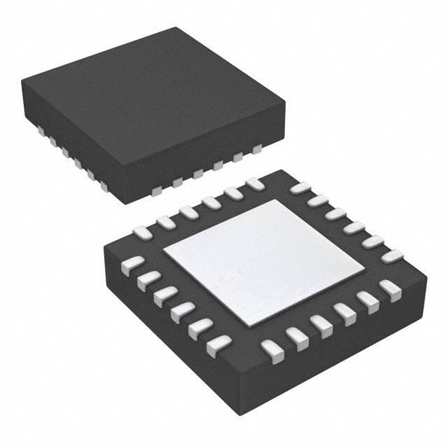
QFN24 4 x 4 x 0.8 mm
Thermal and short-circuit protection of all card
contacts
Card presence detection contacts debounced
Enhanced card side ESD protection of 8 kV
Features
Space saving QFN24 4 x 4 x 0.8 mm package
Complete smartcard interface
ISO 7816, NDS and EMV 4.3 payment systems
compatible
Three protected half-duplex bidirectional
buffered I/O lines to the smartcard
Temperature range -25 to +85 °C
Applications
Smartcard readers for
5 V, 3 V or 1.8 V supply voltage for the
smartcard (VCC), pin-selectable. Ensures
controlled VCC rise and fall times and provides
smart overload detection with glitch immunity.
Set-top boxes
Very low power consumption in deep shutdown
mode
Banking
Pay-TV
Identification
Tachographs
Chip select function allows the device interface
to be isolated from the microcontroller signals allows parallel combination of the card
interface devices (ST8034HC)
Card clock generation by integrated crystal
oscillator or from external clock source
Card clock frequency up to 20 MHz,
programmable by CLKDIV1 and CLKDIV2 pins
(ST8034HN) or by CLKDIV pin (ST8034HC),
with synchronous frequency changes
October 2013
This is information on a product in full production.
DocID024511 Rev 2
1/31
www.st.com
1
�Contents
ST8034HN, ST8034HC
Contents
1
Description . . . . . . . . . . . . . . . . . . . . . . . . . . . . . . . . . . . . . . . . . . . . . . . . . 5
2
Block diagrams . . . . . . . . . . . . . . . . . . . . . . . . . . . . . . . . . . . . . . . . . . . . . 6
3
Pin description . . . . . . . . . . . . . . . . . . . . . . . . . . . . . . . . . . . . . . . . . . . . . 8
4
Maximum ratings . . . . . . . . . . . . . . . . . . . . . . . . . . . . . . . . . . . . . . . . . . . 10
5
Electrical characteristics . . . . . . . . . . . . . . . . . . . . . . . . . . . . . . . . . . . . 11
Electrical characteristics over recommended operating conditions . . . . . . . . . . . 11
6
Functional description . . . . . . . . . . . . . . . . . . . . . . . . . . . . . . . . . . . . . . 19
6.1
Power supplies . . . . . . . . . . . . . . . . . . . . . . . . . . . . . . . . . . . . . . . . . . . . . 19
6.2
Voltage supervisor . . . . . . . . . . . . . . . . . . . . . . . . . . . . . . . . . . . . . . . . . . 19
6.3
Clock circuits . . . . . . . . . . . . . . . . . . . . . . . . . . . . . . . . . . . . . . . . . . . . . . 20
6.4
Input and output circuits . . . . . . . . . . . . . . . . . . . . . . . . . . . . . . . . . . . . . . 21
6.5
Shutdown mode . . . . . . . . . . . . . . . . . . . . . . . . . . . . . . . . . . . . . . . . . . . . 22
6.6
Deep shutdown mode . . . . . . . . . . . . . . . . . . . . . . . . . . . . . . . . . . . . . . . 23
6.7
Activation sequence . . . . . . . . . . . . . . . . . . . . . . . . . . . . . . . . . . . . . . . . . 23
6.8
Deactivation sequence . . . . . . . . . . . . . . . . . . . . . . . . . . . . . . . . . . . . . . . 24
6.9
VCC generator . . . . . . . . . . . . . . . . . . . . . . . . . . . . . . . . . . . . . . . . . . . . . 25
6.10
Fault detection . . . . . . . . . . . . . . . . . . . . . . . . . . . . . . . . . . . . . . . . . . . . . 26
6.11
VCC_SEL pin-programmed card supply voltage (VCC) . . . . . . . . . . . . . . 27
6.12
Chip select (ST8034HC only) . . . . . . . . . . . . . . . . . . . . . . . . . . . . . . . . . . 27
7
Package information . . . . . . . . . . . . . . . . . . . . . . . . . . . . . . . . . . . . . . . . 28
8
Tape and reel information . . . . . . . . . . . . . . . . . . . . . . . . . . . . . . . . . . . . 30
9
Revision history . . . . . . . . . . . . . . . . . . . . . . . . . . . . . . . . . . . . . . . . . . . 30
2/31
DocID024511 Rev 2
�ST8034HN, ST8034HC
List of tables
List of tables
Table 1.
Table 2.
Table 3.
Table 4.
Table 5.
Table 6.
Table 7.
Table 8.
Table 9.
Table 10.
Table 11.
Table 12.
Table 13.
Table 14.
Table 15.
Table 16.
Device summary . . . . . . . . . . . . . . . . . . . . . . . . . . . . . . . . . . . . . . . . . . . . . . . . . . . . . . . . . . 5
Pin description ST8034HN and ST8034HC . . . . . . . . . . . . . . . . . . . . . . . . . . . . . . . . . . . . . 9
Absolute maximum ratings, . . . . . . . . . . . . . . . . . . . . . . . . . . . . . . . . . . . . . . . . . . . . . . . . 10
Thermal data. . . . . . . . . . . . . . . . . . . . . . . . . . . . . . . . . . . . . . . . . . . . . . . . . . . . . . . . . . . . 10
Recommended operating conditions . . . . . . . . . . . . . . . . . . . . . . . . . . . . . . . . . . . . . . . . . 10
Supply voltages . . . . . . . . . . . . . . . . . . . . . . . . . . . . . . . . . . . . . . . . . . . . . . . . . . . . . . . . . 11
Card interface . . . . . . . . . . . . . . . . . . . . . . . . . . . . . . . . . . . . . . . . . . . . . . . . . . . . . . . . . . . 13
Microcontroller interface . . . . . . . . . . . . . . . . . . . . . . . . . . . . . . . . . . . . . . . . . . . . . . . . . . . 15
Clock circuits. . . . . . . . . . . . . . . . . . . . . . . . . . . . . . . . . . . . . . . . . . . . . . . . . . . . . . . . . . . . 17
Protection characteristics . . . . . . . . . . . . . . . . . . . . . . . . . . . . . . . . . . . . . . . . . . . . . . . . . . 17
Timing characteristics . . . . . . . . . . . . . . . . . . . . . . . . . . . . . . . . . . . . . . . . . . . . . . . . . . . . . 18
Clock frequency selection . . . . . . . . . . . . . . . . . . . . . . . . . . . . . . . . . . . . . . . . . . . . . . . . . . 21
VCC selection by VCC_SEL1, VCC_SEL2 pins . . . . . . . . . . . . . . . . . . . . . . . . . . . . . . . . . 27
QFN24 4 x 4 x 0.8 mm, 0.5 mm pitch package mechanical data, . . . . . . . . . . . . . . . . . . . 29
Tape and reel specification for QFN24 . . . . . . . . . . . . . . . . . . . . . . . . . . . . . . . . . . . . . . . . 30
Document revision history . . . . . . . . . . . . . . . . . . . . . . . . . . . . . . . . . . . . . . . . . . . . . . . . . 30
DocID024511 Rev 2
3/31
�List of figures
ST8034HN, ST8034HC
List of figures
Figure 1.
Figure 2.
Figure 3.
Figure 4.
Figure 5.
Figure 6.
Figure 7.
Figure 8.
Figure 9.
Figure 10.
Figure 11.
Figure 12.
Figure 13.
Figure 14.
Figure 15.
Figure 16.
4/31
Block diagram ST8034HN . . . . . . . . . . . . . . . . . . . . . . . . . . . . . . . . . . . . . . . . . . . . . . . . . . 6
Block diagram ST8034HC . . . . . . . . . . . . . . . . . . . . . . . . . . . . . . . . . . . . . . . . . . . . . . . . . . 7
Pin connections ST8034HN (top-through view) . . . . . . . . . . . . . . . . . . . . . . . . . . . . . . . . . . 8
Pin connections ST8034HC (top-through view) . . . . . . . . . . . . . . . . . . . . . . . . . . . . . . . . . . 8
Definition of duty cycle and input and output rise/fall times . . . . . . . . . . . . . . . . . . . . . . . . 18
Voltage supervisor, configured with adjustable VDD(INTF) threshold. . . . . . . . . . . . . . . . . . 19
Voltage supervisor waveforms . . . . . . . . . . . . . . . . . . . . . . . . . . . . . . . . . . . . . . . . . . . . . . 20
External clock usage. . . . . . . . . . . . . . . . . . . . . . . . . . . . . . . . . . . . . . . . . . . . . . . . . . . . . . 21
Shutdown and deep shutdown mode activation and deactivation . . . . . . . . . . . . . . . . . . . 23
Activation sequence . . . . . . . . . . . . . . . . . . . . . . . . . . . . . . . . . . . . . . . . . . . . . . . . . . . . . . 24
Deactivation sequence . . . . . . . . . . . . . . . . . . . . . . . . . . . . . . . . . . . . . . . . . . . . . . . . . . . . 25
Deactivation sequence after card removal . . . . . . . . . . . . . . . . . . . . . . . . . . . . . . . . . . . . . 26
Debounce at OFF, CMDVCC, PRES and VCC pins . . . . . . . . . . . . . . . . . . . . . . . . . . . . . . 27
QFN24 4 x 4 x 0.8 mm, 0.5 mm pitch package outline . . . . . . . . . . . . . . . . . . . . . . . . . . . . 28
QFN24 recommended footprint . . . . . . . . . . . . . . . . . . . . . . . . . . . . . . . . . . . . . . . . . . . . . 29
Carrier tape for QFN24 . . . . . . . . . . . . . . . . . . . . . . . . . . . . . . . . . . . . . . . . . . . . . . . . . . . . 30
DocID024511 Rev 2
�ST8034HN, ST8034HC
1
Description
Description
The ST8034HN and ST8034HC devices are complete low-cost analog interfaces for
asynchronous and synchronous smartcards operating at a supply voltage of 5 V, 3 V or
1.8 V. The ST8034HN and ST8034HC devices can be placed between the card and the
microcontroller to provide all supply, protection, detection and control functions, with just
a few external components.
Table 1. Device summary
VCC
Chip CLKDIV
NDS
selection
select inputs compliant
pins
Order code
PORADJ
ST8034HNQR
ST8034HCQR
Package
Shipment
Package
topmark
2
QFN24
4 x 4 x 0.85 mm,
0.5 mm pitch
Tape and
reel
8034HN
1
QFN24
4 x 4 x 0.85 mm,
0.5 mm pitch
Tape and
reel
8034HC
DocID024511 Rev 2
5/31
�Block diagrams
2
ST8034HN, ST8034HC
Block diagrams
Figure 1. Block diagram ST8034HN
����Q)
9''
��
9''�,17)�
5�
567,1
&0'9&&
2))
&/.',9�
&/.',9�
9&&B6(/�
9&&B6(/�
,�28&
$8;�8&
$8;�8&
9''3
��
��
,17(51$/��
5()(5(1&(
325$'- ��
35(6
*1'
6833/<
5�
���
����Q)
92/7$*(�
6(16(
,17(51$/��
26&,//$725
&/.83
(1�
$/$50
�
39&&
�
6(48(1&(5
�
��
(1�
9&&
/'2
�� 9&&
5(6(7�
*(1(5$725
�� 567
&/2&.�
*(1(5$725
�� &/.
����Q)
(1�
&/2&.�
&,5&8,7
�
&/.
(1�
����Q)
�
�
/(9(/
6+,)7(5
�
&5 2 V
0.75
VDD(INTF)
VDD(INTF)
+ 0.1
IOH -20 A;
VDD(INTF) < 2 V
0.75
VDD(INTF)
VDD(INTF)
+ 0.1
VOH
Output voltage high
IOL = 1 mA
V
VIL
Input voltage low
-0.3
0.3
VDD(INTF)
V
VIH
Input voltage high
0.7
VDD(INTF)
VDD(INTF)
+ 0.3
V
VHYS
0.14
VDD(INTF)
Hysteresis
I/OUC pin
V
IIL
Input current low
VIL = 0 V
500
A
IIH
Input current high
VIH = VDD(INTF)
10
A
12
k
RPU
Pull-up resistance to
VDD(INTF)
8
IPU
Pull-up current (one-shot
VOH = 0.9 VDD(INTF)
circuit active)
-1
tR(I)
Input rise time
VIL max. to VIH min.
0.15
s
tR(O)
Output rise time
CL 30 pF, 10% to 90%, 0 V
to VDD(INTF)
0.1
s
tF(I)
Input fall time
VIL max. to VIH min.
0.15
s
tF(O)
Output fall time
CL 30 pF, 10% to 90%, 0 V
to VDD(INTF)
0.1
s
10
mA
Device control inputs (CLKDIV1, CLKDIV2, RSTIN, VCC_SEL1, VCC_SEL2, CS pins)(3)
VIL
Input voltage low
-0.3
0.3
VDD(INTF)
V
VIH
Input voltage high
VDD(INTF)
VDD(INTF)
+ 0.3
V
VHYS
0.14
VDD(INTF)
Hysteresis
DocID024511 Rev 2
V
15/31
�Electrical characteristics
ST8034HN, ST8034HC
Table 8. Microcontroller interface (continued)
Symbol
Parameter
Test conditions(1)
Min.
Typ.
Max.
Unit
IIL
Input current low
1
A
IIH
Input current high
1
A
(4)
Control input CMDVCC
VIL
Input voltage low
-0.3
0.3
VDD(INTF)
V
VIH
Input voltage high
0.7
VDD(INTF)
VDD(INTF)
+ 0.3
V
VHYS
0.14
VDD(INTF)
Hysteresis
V
IIL
Input current low
VIL = 0 V
1
A
IIH
Input current high
VIH = VDD(INTF)
1
A
100
Hz
0.3
V
fCMDVCC
Frequency at CMDVCC
pin
OFF output(5)
VOL
Output voltage low
IOL = 2 mA
VOH
Output voltage high
IOH = -15 A
RPU
Pull-up resistance to
VDD(INTF)
0
0.75
VDD(INTF)
16
V
20
24
k
1. TA = 25 °C, VDD = 3.3 V, VDDP = 5 V, VDD(INTF) = 3.3 V, fXTAL = 10 MHz, unless otherwise noted.
2. With an internal 10 k pull-up resistor to VDD(INTF).
3. For clock frequency division control (CLKDIV), see Table 12 on page 21.
4. CMDVCC is active low.
5. OFF is an NMOS open drain, with an internal 20 k pull-up resistor to VDD(INTF). The pull-up is connected only when used
(i.e. when OFF = high), otherwise disconnected.
16/31
DocID024511 Rev 2
�ST8034HN, ST8034HC
Electrical characteristics
Table 9. Clock circuits
Symbol
Test conditions(1)
Parameter
Min.
Typ.
Max.
Unit
100
150
200
kHz
2
2.7
3.2
MHz
15
pF
2
26
MHz
0.032
26
MHz
Internal oscillator
fOSC(INT)LOW
fOSC(INT)
Shutdown mode
Internal oscillator frequency
Active state
Crystal oscillator (XTAL1 and XTAL2 pins)
CEXT
External capacitances
XTAL1 and XTAL2 to GND
(according to the crystal or
resonator specification)
fXTAL
External crystal frequency
Card clock reference,
crystal oscillator
fEXT
External clock frequency
External clock on XTAL1
tR(fEXT)
External clock frequency rise time External clock on XTAL1
10
ns
tF(fEXT)
External clock frequency fall time External clock on XTAL1
10
ns
VIL
Input voltage low
VIH
Input voltage high
Crystal oscillator
-0.3
0.3 VDD
External clock on XTAL1
-0.3
0.3
VDD(INTF)
0.7 VDD
VDD + 0.3
0.7
VDD(INTF)
+ 0.3
V
Max.
Unit
Crystal oscillator
External clock on XTAL1
VDD(INTF)
V
1. TA = 25 °C, VDD = 3.3 V, VDDP = 5 V, VDD(INTF) = 3.3 V, fXTAL = 10 MHz, unless otherwise noted.
Table 10. Protection characteristics
Symbol
IOLIM
Test conditions(1)
Parameter
Output current limit
(2)
ISD(VCC)
Limit and shutdown card supply
current
TSD
Shutdown junction temperature
Min.
Typ.
I/O pin
-15
15
CLK pin
-70
70
RST pin
-20
20
VCC pin
90
120
150
150
mA
mA
°C
1. TA = 25 °C, VDD = 3.3 V, VDDP = 5 V, VDD(INTF) = 3.3 V, fXTAL = 10 MHz, unless otherwise noted.
2. All card contacts are protected against short-circuit to any other card contact.
DocID024511 Rev 2
17/31
�Electrical characteristics
ST8034HN, ST8034HC
Table 11. Timing characteristics
Symbol
tACT
tDEACT
tD(START),
tD(END)
Test conditions(1)
Parameter
Activation time
See Figure 10 on
page 24
2090
Deactivation time
See Figure 11 on
page 25
35
tD(START) = t3,
see Figure 10 on
Delay time, CLK sent to card using an page 24
external clock
=t ,
t
D(END)
5
see Figure 10 on
page 24
tDEB
Min.
Debounce time
PRES pin
Typ.
90
2090
Max.
Unit
4160
µs
250
µs
4112
µs
2120
3.2
4160
4.5
6.4
ms
1. TA = 25 °C, VDD = 3.3 V, VDDP = 5 V, VDD(INTF) = 3.3 V, fXTAL = 10 MHz, unless otherwise noted.
Figure 5. Definition of duty cycle and input and output rise/fall times
W)
W5
���
92+
���
�92+���92/�����
���
���
W�
W�
92/
$0�����
Duty cycle (DC) = t1 / (t1 + t2).
18/31
DocID024511 Rev 2
�ST8034HN, ST8034HC
6
Functional description
Functional description
Throughout this document it is assumed that the reader is familiar with ISO7816
terminology.
6.1
Power supplies
All interface signals to the host microcontroller are referenced to VDD(INTF). All card contacts
remain inactive during power-up or power-down. After powering up the device, OFF output
remains low until CMDVCC input is set high and PRES input is low. During power-down,
OFF output goes low when VDDP falls below the VDDP falling threshold voltage. The internal
oscillator clock frequency fOSC(INT) is used only during the activation sequence. When the
card is not activated (CMDVCC input is high), the internal oscillator is in low frequency
mode to reduce power consumption.
Power-on sequence: supply voltages may be applied to the ST8034 in any sequence.
6.2
Voltage supervisor
Figure 6. Voltage supervisor, configured with adjustable VDD(INTF) threshold
9''�,17)�
9''�,17)�
5�
325$'-
�
�
9''
5�
9''
5()(5(1&(
92/7$*(
�
�
9''3
�
�
9&&B6(/�
$0�����
DocID024511 Rev 2
19/31
�Functional description
ST8034HN, ST8034HC
The voltage supervisor monitors the VDDP, VDD, and VDD(INTF) voltages and provides both
power-on reset (POR) and supply dropout detection during a card session. The supervisor
threshold voltages for VDDP and VDD are set internally, and VDD(INTF) is set externally by an
external resistor divider on the PORADJ pin, which provides additional voltage monitoring
flexibility (this pin can be used for monitoring any external voltage, with adjustable
threshold):
Undervoltage (UVLO) threshold adjustment on the PORADJ input with the resistor divider:
VDD(INTF) UVLO threshold (falling) = (R1+R2)/R2 x VTH(PORADJ)
VDD(INTF) UVLO threshold (rising) = (R1+R2)/R2 x (VTH(PORADJ) + VHYST(PORADJ))
If the external resistor divider is not used, connect the PORADJ pin to VDD(INTF), then
VDD(INTF) UVLO threshold = VTH(PORADJ).
As long as VDDP, VDD or VDD(INTF) is less than the corresponding VTH + VHYS, the device
remains inactive irrespective of the command line levels. After VDDP, VDD, and VDD(INTF)
has reached a level higher than the corresponding VTH + VHYS, the device still remains
inactive for the duration of tW, a defined reset pulse of approximately 8 ms (tW = 1024 x
1/fOSC(INT)LOW) when the output of the supervisor keeps the control logic in reset state. This
is used to maintain the device in shutdown mode during the supply voltage power-on, see
Figure 7. A deactivation sequence is performed when either VDD, VDDP or VDD(INTF) falls
below the corresponding VTH.
Figure 7. Voltage supervisor waveforms
97+���9+ t3 and < t5
t5 (tD(END)) = t1 + 23T/2.
T = 64 x 1/fOSC(INT).
Figure 10. Activation sequence
&0'9&&
;7$/
9&&
�
$75
,�2
&/.
!�����QV
567,1
567
,�28&
,17(51$/
26&,//$725�
ORZ�IUHTXHQF\
W�
KLJK�IUHTXHQF\
W�� �W�
W� W�� �W'�(1'�� ��W$&7
W�� �W'�67$57�
$0�����
6.8
Deactivation sequence
When a session ends, the microcontroller sets CMDVCC high. The ST8034 device then
executes an automatic deactivation sequence by counting the sequencer back to the
inactive state (see Figure 11):
24/31
1.
RST goes low (t11).
2.
The clock is stopped, CLK is low (t12).
3.
I/O, AUX1, AUX2 are pulled low (t13).
4.
VCC falls to 0 V (t14). The deactivation sequence is completed when VCC reaches its
inactive state.
5.
VCC < 0.4 V (tDEACT).
6.
All card contacts become low impedance to GND. The I/OUC, AUX1UC and AUX2UC
pins remain pulled up to VDD(INTF) by the internal 10 k pull-up resistor.
7.
The internal oscillator returns to its low frequency mode.
DocID024511 Rev 2
�ST8034HN, ST8034HC
Functional description
Time delays
t11 = t10 + 3T / 64
t12 = t11 + T / 2
t13 = t11 + T
t14 = t11 + 3T / 2
tDEACT = t11 + 3T / 2 + VCC fall time.
T = 64 x 1/fOSC(INT).
Figure 11. Deactivation sequence
&0'9&&
567
&/.
,�2
9&&
;7$/�
,17(51$/�
26&,//$725
KLJK�IUHTXHQF\
W�� W������������ W��
ORZ�IUHTXHQF\
W��
W��
W'($&7
$0�����
6.9
VCC generator
The LDO on the VCC output is capable of supplying up to 65 mA continuously at any
selected VCC value (5 V, 3 V or 1.8 V). This output is overcurrent protected by the current
limiter with a limit threshold value of 120 mA typ., with a glitch immunity allowing overcurrent
pulses up to 200 mA with duration up to several microseconds not causing a deactivation
(the average current value must stay below the specified current limit, see Table 6 on
page 11 and Table 10 on page 17).
A 100 nF capacitor (min.) with ESR < 350 m should be tied to GND near the VCC pin and
another low ESR 100 nF capacitor (min.) should be tied to GND also on the card side, near
the card reader contact C1.
DocID024511 Rev 2
25/31
�Functional description
6.10
ST8034HN, ST8034HC
Fault detection
The fault conditions monitored by the device are:
Short-circuit or overcurrent on the VCC pin
Card removal during transaction
VDD falling
VDDP falling
VDD(INTF) falling
Overheating.
There are two different fault detection situations:
Outside card session (CMDVCC pin is high): the OFF pin is low if the card is not in the
reader and high if the card is in the reader. Any voltage drop on VDD, VDDP or VDD(INTF)
is detected by the voltage supervisor. This generates an internal power-on reset pulse
but does not act upon the OFF pin signal. The card is not powered-up and short-circuits
or overheating are not detected.
In card session (CMDVCC pin is low): when the OFF pin goes low, the fault detection
circuit triggers the automatic emergency deactivation sequence (see Figure 12).
On card insertion or removal, bouncing can occur on the card presence switch (i.e. on the
PRES signal). Therefore a debouncing feature is integrated into the ST8034 (4.5 ms
typically, tDEB = 640 × 1/fOSC(INT)LOW). See Figure 13.
On card insertion, the OFF pin goes high after the debounce time has elapsed. When the
card is extracted, the automatic card deactivation sequence is performed on the first high to
low transition on the PRES pin. After this, the OFF pin goes low.
Figure 12. Deactivation sequence after card removal
2))
35(6�
567
&/.
,�2
9&&
;7$/�
,17(51$/
26&,//$725
�
KLJK�IUHTXHQF\
W��
�W��
ORZ�IUHTXHQF\
W��
W��
W'($&7
$0�����
26/31
DocID024511 Rev 2
�ST8034HN, ST8034HC
Functional description
Figure 13. Debounce at OFF, CMDVCC, PRES and VCC pins
35(6
2))
&0'9&&
W
�
W
'(%
'(%
�
���
9&&
���
$0�����
1. Deactivation caused by card withdrawal.
2. Deactivation caused by short-circuit on card side.
6.11
VCC_SEL pin-programmed card supply voltage (VCC)
The card supply voltage (VCC) is selected by the VCC_SEL1 and VCC_SEL2 inputs, see
Table 13.
Table 13. VCC selection by VCC_SEL1, VCC_SEL2 pins
VCC_SEL1 pin level
VCC_SEL2 pin level
VCC
Low
x(1)
1.8 V
High
High
5V
High
Low
3V
1. x = “don't care”. However keep in mind that combination VCC_SEL1 = VCC_SEL2 = GND and CMDVCC =
high initiates deep shutdown mode.
6.12
Chip select (ST8034HC only)
The chip select (CS) input pin of the ST8034HC replaces the CLKDIV1 pin and is active
high, meaning normal operation of the device when CS is in logic high state. When the CS
pin goes low, the status of the ST8034HC device is frozen (i.e. status of control inputs
RSTIN, CMDVCC, CLKDIV, VCC_SEL1 and VCC_SEL2 is latched) and the I/OUC,
AUX1UC, and AUX2UC pins on the microcontroller interface go into high impedance mode
(with pull-up resistors to VDD(INTF)), not transferring any data to or from the card. The OFF
output pin also goes into high impedance mode. This allows the microcontroller to share
interface pins among multiple smartcard interfaces connected in parallel. Status and all the
ST8034HC device functions (including the card) are maintained for immediate use when the
CS goes high again. For this reason clock input is not affected by the chip select, the clock
is provided to the ST8034HC device and to the card even when the CS is low.
DocID024511 Rev 2
27/31
�Package information
7
ST8034HN, ST8034HC
Package information
In order to meet environmental requirements, ST offers these devices in different grades of
ECOPACK® packages, depending on their level of environmental compliance. ECOPACK
specifications, grade definitions and product status are available at: www.st.com.
ECOPACK is an ST trademark.
Figure 14. QFN24 4 x 4 x 0.8 mm, 0.5 mm pitch package outline
723�9,(:
'
�
$
,QGH[�DUHD
%
�'��[(���
(
DDD & �[
DDD & �[
6,'(�9,(:
FFF &
&
$
�
��[
HHH &
$�
%27720�9,(:
H
�
6($7,1*�
3/$1(
�
E
��[
��
EEE 0 & $ %
GGG 0 &
/
��[ �
��
(�
��
�
3,1���,'
5�����
��
��
.
��[
'�
4)1��
28/31
DocID024511 Rev 2
�ST8034HN, ST8034HC
Package information
Table 14. QFN24 4 x 4 x 0.8 mm, 0.5 mm pitch package mechanical data(1), (2)
Dimensions (mm)
Symbol
Note
Min.
Typ.
Max.
A
0.80
0.90
1.00
A1
0.00
0.02
0.05
b
0.18
0.25
0.30
D
3.90
4.00
4.10
E
3.90
4.00
4.10
e
(3)
0.5 ref.
D2
1.95
2.10
2.20
E2
1.95
2.10
2.20
K
0.20
-
-
L
0.30
0.40
0.50
aaa
0.05
0.05
bbb
0.10
0.10
ccc
0.10
0.10
ddd
0.05
0.05
eee
0.08
0.08
1. Dimensioning and tolerancing conform to ASME Y14.5-2009.
2. The location of the terminal #1 identifier is within the hatched area.
3. Dimension b applies to metallized terminal. If the terminal has a radius on its end, dimension b should not
be measured in that radius area.
Figure 15. QFN24 recommended footprint
����
����
��
��
����
�
��
����
����
�
��
����
�
��
����
DocID024511 Rev 2
29/31
�Tape and reel information
8
ST8034HN, ST8034HC
Tape and reel information
Figure 16. Carrier tape for QFN24
����
�������
�������������
����������
$
�����PLQ�
����������
5�����PD[�
������
�����
��������� ����
%R
�����
.R
$
$R
$R� �����
%R� �����
.R� �����
6HFWLRQ�$���$
5������
1. 10 sprocket hole pitch cumulative tolerance 0.2.
2. Camber in compliance with EIA 481.
3. Pocket position relative to sprocket hole measured as true position of pocket, not pocket hole.
Table 15. Tape and reel specification for QFN24
Carrier tape
Quantity
per reel
3000
9
Cover tape
Lockreel 7 / 13"
Part no.
(vendor)
Description
Part no.
(vendor)
Description
Part no.
(vendor)
Description
434146 (Cpak)
Carrier tape
12 mm width,
8 mm pitch
437150 (Cpak)
Cover tape
9.2 mm width
434543 (peak)
13" lockreel
Revision history
Table 16. Document revision history
Date
Revision
22-Apr-2013
1
Initial release.
22-Oct-2013
2
Updated title on page 1 (removed ST8034HN and ST8034HC).
Updated Table 1 on page 5 (removed note 1).
Minor modifications throughout document.
30/31
Changes
DocID024511 Rev 2
�ST8034HN, ST8034HC
Please Read Carefully:
Information in this document is provided solely in connection with ST products. STMicroelectronics NV and its subsidiaries (“ST”) reserve the
right to make changes, corrections, modifications or improvements, to this document, and the products and services described herein at any
time, without notice.
All ST products are sold pursuant to ST’s terms and conditions of sale.
Purchasers are solely responsible for the choice, selection and use of the ST products and services described herein, and ST assumes no
liability whatsoever relating to the choice, selection or use of the ST products and services described herein.
No license, express or implied, by estoppel or otherwise, to any intellectual property rights is granted under this document. If any part of this
document refers to any third party products or services it shall not be deemed a license grant by ST for the use of such third party products
or services, or any intellectual property contained therein or considered as a warranty covering the use in any manner whatsoever of such
third party products or services or any intellectual property contained therein.
UNLESS OTHERWISE SET FORTH IN ST’S TERMS AND CONDITIONS OF SALE ST DISCLAIMS ANY EXPRESS OR IMPLIED
WARRANTY WITH RESPECT TO THE USE AND/OR SALE OF ST PRODUCTS INCLUDING WITHOUT LIMITATION IMPLIED
WARRANTIES OF MERCHANTABILITY, FITNESS FOR A PARTICULAR PURPOSE (AND THEIR EQUIVALENTS UNDER THE LAWS
OF ANY JURISDICTION), OR INFRINGEMENT OF ANY PATENT, COPYRIGHT OR OTHER INTELLECTUAL PROPERTY RIGHT.
ST PRODUCTS ARE NOT DESIGNED OR AUTHORIZED FOR USE IN: (A) SAFETY CRITICAL APPLICATIONS SUCH AS LIFE
SUPPORTING, ACTIVE IMPLANTED DEVICES OR SYSTEMS WITH PRODUCT FUNCTIONAL SAFETY REQUIREMENTS; (B)
AERONAUTIC APPLICATIONS; (C) AUTOMOTIVE APPLICATIONS OR ENVIRONMENTS, AND/OR (D) AEROSPACE APPLICATIONS
OR ENVIRONMENTS. WHERE ST PRODUCTS ARE NOT DESIGNED FOR SUCH USE, THE PURCHASER SHALL USE PRODUCTS AT
PURCHASER’S SOLE RISK, EVEN IF ST HAS BEEN INFORMED IN WRITING OF SUCH USAGE, UNLESS A PRODUCT IS
EXPRESSLY DESIGNATED BY ST AS BEING INTENDED FOR “AUTOMOTIVE, AUTOMOTIVE SAFETY OR MEDICAL” INDUSTRY
DOMAINS ACCORDING TO ST PRODUCT DESIGN SPECIFICATIONS. PRODUCTS FORMALLY ESCC, QML OR JAN QUALIFIED ARE
DEEMED SUITABLE FOR USE IN AEROSPACE BY THE CORRESPONDING GOVERNMENTAL AGENCY.
Resale of ST products with provisions different from the statements and/or technical features set forth in this document shall immediately void
any warranty granted by ST for the ST product or service described herein and shall not create or extend in any manner whatsoever, any
liability of ST.
ST and the ST logo are trademarks or registered trademarks of ST in various countries.
Information in this document supersedes and replaces all information previously supplied.
The ST logo is a registered trademark of STMicroelectronics. All other names are the property of their respective owners.
© 2013 STMicroelectronics - All rights reserved
STMicroelectronics group of companies
Australia - Belgium - Brazil - Canada - China - Czech Republic - Finland - France - Germany - Hong Kong - India - Israel - Italy - Japan Malaysia - Malta - Morocco - Philippines - Singapore - Spain - Sweden - Switzerland - United Kingdom - United States of America
www.st.com
DocID024511 Rev 2
31/31
�


 工商网监
湘ICP备2023018690号
工商网监
湘ICP备2023018690号
